N. kumar 1, U. Parihar 1, R. Kumar 1, K. J. Patel 2, C. J. Panchal 2, N. Padha 1
1Department of Physics and Electronics, Ambedkar Road, University of Jammu, Jammu, 180006, India
2Applied Physics Department, Faculty of Technology and Engineering, M.S. University of Baroda, Vadodara, 390001, India
Correspondence to: C. J. Panchal , Applied Physics Department, Faculty of Technology and Engineering, M.S. University of Baroda, Vadodara, 390001, India.
| Email: |  |
Copyright © 2012 Scientific & Academic Publishing. All Rights Reserved.
Abstract
Tin Selenide (SnSe) thin films were prepared from the pulverized compound material by thermal evaporation method, to study the effect of film thickness on its structural, and optical properties. The different thicknesses of SnSe thin films, from 150 nm to 500 nm, were grown on glass substrate held at room temperature. X-ray diffraction, atomic force microscopy, transmission measurement, and four-point probe method were used to characterize the thin films. The optical transmission spectra suggests, the energy band gap decreases with increasing the film thickness. The electrical resistivity shows that the films were semi-conducting in behavior having p-type conductivity.
Keywords:
Tin Selenide (SnSe) thin film, Thermal evaporation method, XRD, AFM, Optical properties
Cite this paper:
N. kumar , U. Parihar , R. Kumar , K. J. Patel , C. J. Panchal , N. Padha , "Effect of Film Thickness on Optical Properties of Tin Selenide Thin Films Prepared by Thermal Evaporation for Photovoltaic Applications", American Journal of Materials Science, Vol. 2 No. 1, 2012, pp. 41-45. doi: 10.5923/j.materials.20120201.08.
1. Introduction
Tin Selenide (SnSe) is a narrow band gap, binary IV–VI semiconductor, suitable for various optoelectronic applications like memory switching devices, photovoltaic, light emitting devices (LED), and holographic recording systems [1-3]. Large availability of constituents of SnSe compound in nature has been raised attention for the cost effective solution in photovoltaic applications. Recently, N.R. Mathews was reported for the first time a CdS/SnSe solid state heterojunction solar cell[2]. SnSe has a orthorhombic crystallographic structure with lattice parameters: a = 11.50 Å, b = 4.15 Å, and c = 4.44 Å, which may be viewed as a distorted NaCl rock-salt structure in order to obtain layers made up of double planes[4]. The structure of the SnSe thin films strongly influences the optical and electrical properties, which is dependent on the preparation technique. Various deposition techniques are reported for the preparation of SnSe thin films viz. chemical bath deposition[5], atomic layer deposition[6], thermal evaporation[7-8], Hot wall epitaxy[9], flash evaporation[10]. Among them, the thermal evaporation is most commonly employed method because it is very simple, economical, and convenient technique, mostly used in the production of large-area devices. We already reported the effect of substrate temperature on the properties of SnSe thin film[11]. In the present work, SnSe thin films were grown by thermal evaporation method and study the effect of the film thickness on the structural, morphological, and optical properties.
2. Experimental Details
The SnSe thin films were grown at room temperature by thermal evaporation of fine-grained pulverized SnSe powder (Alfa Aesar, 99.999%) on organically cleaned soda-lime glass substrate. The base pressure during the deposition was 10−5 mbar achieved by a high-vacuum coating unit (Hindhivac, Model-12-A4D). The film of different thickness from 150 - 500 nm were deposited at a constant rate of 0.3 nm/s, which was monitored using quartz crystal based thin film deposition controller (Hindhivac, DTM -101).The structural characterization was carried out using a Rigaku D-Max-III X-ray diffractometer, in 2θ range of 20°-50°, at a scan-rate of 0.05° s-1 using CuKα (λ = 0.154 nm) radiation. Surface morphology of the deposited films was observed using atomic force microscopy (AFM). Optical transmittance spectra of the thin films were measured in the photon energy range of 0.8-2.5 eV. The transmittance measurement setup consists of Tungsten-Halogen light source, monochromator (CM110), chopper, Silicon photo- detectors, a lock-in amplifier (SR-530). The whole optical setup was automated using LabVIEW (Version 8.2) program. The temperature dependence of electrical conductivity in the range 300-450 K was carried out by the four-point probe method, consisting of digital low current source (Model LCS-002), digital millivoltmeter (Model DMV-001) and PID based temperature controlled oven (Model PID-200).
3. Results and Discussions
3.1. X-ray Diffraction Measurement
X-ray diffraction (XRD) patterns of SnSe thin films having 150 nm and 500 nm thickness, deposited at room temperature are shown in Figure 1.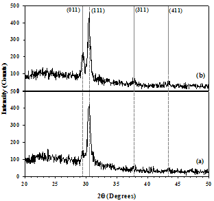 | Figure 1. XRD patterns of SnSe thin films of thickness (a) 150 nm, and (b) 500 nm deposited at room temperature |
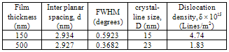
The as-deposited SnSe thin films have an orthorhombic crystal structure. The diffraction peaks correspond to (011), (111), (311), and (411) reflections of the orthorhombic phase at around 2θ of 29.5°, 30.5°, 37.8°, and 43.4°, respectively, which is a good agreement with the standard JCPDS data [card no. 32-1382]. The preferred orientation along (111) plane increased with increase in the film thickness, which indicates improvement in crystallinity. A similar result with preferred orientation of (111) plane was also reported by Singh and Bedi[9] and Z. Zainal et al.[12] for the SnSe thin films grown by the vacuum evaporation technique. The inter-planar spacing (dhkl) calculated for the (111) plane having different film thickness using the Bragg’s relation are presented in Table 1. The crystalline size was estimated from the full width at half maximum (FWHM) of the (111) peak using Scherrer’s formula[13]. | (1) |
where, λ is the wavelength of the X-ray, θ is Bragg’s angle, and β is the FWHM of (111) peak.The dislocation density (δ) defined as the length of dislocation lines per unit volume of the crystal is given by the Williamson and Smallman’s relation[14], | (2) |
where, n equals to unity, giving a minimum dislocation density and D is the crystalline size. The values of crystalline size (D) and dislocation density (δ) are also given in the Table 1.Table 1. Structural Parameters viz. Inter-planar Spacing, Crystalline Size, and Dislocation Density of SnSe Thin Films Deposited at Room Temperature, Oriented Along (111) Direction Planes
 |
| |
|
It is observed that the crystalline size increases from 15 to 23 nm with the increase in film thickness from 150 to 500 nm. In polycrystalline samples, dislocated atoms occupy the regions near the grain boundary. Generally the dislocation density is inversely proportional to crystalline size so it was observed that dislocation density decreased with increase in film thickness.
3.2. Atomic Force Microscopy Measurement
The surface morphology of the SnSe thin films was observed using atomic force microscopy technique. Figure 2 shows the three-dimensional (3D) images of SnSe thin films prepared by thermal evaporation techniques with 150 nm and 500 nm film thickness. 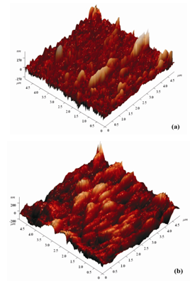 | Figure 2. AFM images of SnSe thin films of thickness (a) 150 nm, and (b) 500 nm deposited at room temperature |
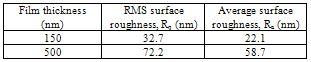
The SnSe thin films having 150 nm thickness showed that the growth of non-uniform grains was distributed across the surface of the substrate. However, the size of the grains was noticed to increase with the corresponding increase in thickness of the film. The films deposited at higher thickness of the order of around 500 nm shows compact surface morphology. AFM image shows that as the thickness increased the smaller grains agglomerate together to form larger grains, which, result in the increased grain size of the film. On the other hand the root-mean-square (RMS) surface roughness (Rq) and average surface roughness (Ra) value, on an area of 5μm × 5μm, using AFM technique is shown in Table 2.Table 2. RMS Surface Roughness and Average Surface Roughness Value of Snse Thin Films
 |
| |
|
The surface roughness of the SnSe film increases with the increase in film thickness and at 500 nm, RMS surface roughness reaches maximum value of 72.2 nm. The surface roughness was apparently changed since the grain growth takes place with increase in film thickness.
3.3. Optical Measurement
The optical transmission spectra of the SnSe thin films with different thicknesses are shown in Figure 3. The films visually found to be blackish gray in color with good adhesion to the substrate. It is evident that the transmittance of the SnSe thin film decreases with increase in the film thickness. The higher transmittance of 150 nm film thickness is due to the smoother surface observed by AFM measurement and the less adsorbed states would be present. The smoother surface reduces the reflection loss due to roughness-induced surface scattering and at lower thickness the density of localized state is also less. As the thickness increases the surface roughness and density of localized state increases which, reduces the transmittance value.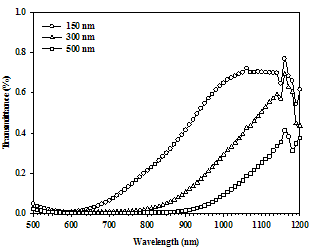 | Figure 3. Transmission spectra for different thicknesses of SnSe thin films deposited at room temperature |
The optical energy band gap of the SnSe thin film was calculated using the Tauc’s relation[15], given bywhere B is a constant, hν is the incident photon energy, Eg is the optical energy band gap, and α is the absorption coefficient; here α = -ln(T)/d, where T is transmittance and d is the thickness of the thin film. The exponent η depends upon the type of optical transition in the material. In case of the SnSe, η is equal to 1/2, for direct allowed transitions. Thus, the optical energy band gap of SnSe was determined by plotting (αhν)2 versus the incident photon energy (hν), and by extrapolating the curve to αhν = 0 as shown in Figure 4.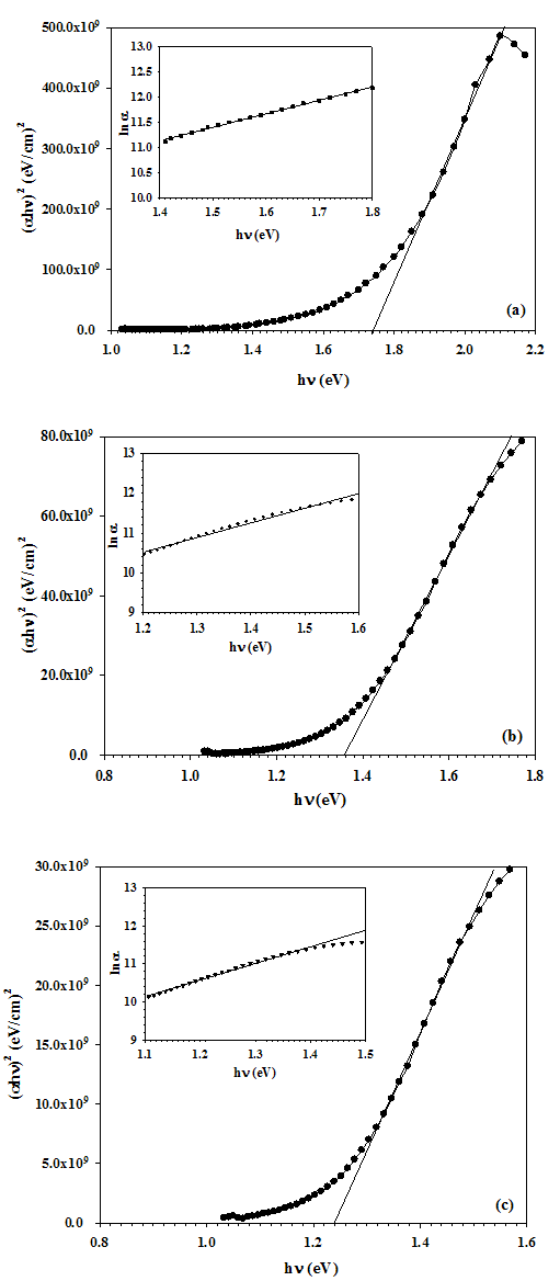 | Figure 4. The plots of (αhν)2 vs. photon energy (hν) (main plot) and their respective plots of ln(α) vs. photon energy (hν) (inset plot) for different thicknesses (a) 150 nm, (b) 300 nm, and (c) 500 nm of SnSe thin films |
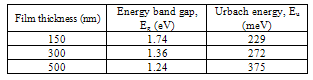
The value of optical energy band gap found to be decreasing from 1.74 to 1.24 eV as the film thickness increases from 150 to 500 nm, which shows its capability to be used as an absorber layer in photovoltaic application. In general, the density of localized state in the film increases with the film thickness which leads to decrease in the band gap. Such a variation in energy band gap with the increase thickness in TiO2-SnO2 thin films has been reported by S. Sonmezoglu et al.[16].It is assumed that the absorption coefficient (α) near the band edge shows an exponential dependence on photon energy for many materials. This dependence is given as follows[17],where, αo is a constant and Eu is Urbach energy which is the width of the tail of the localized state associated with the amorphous state in the forbidden band. The plot of ln(α) vs. photon energy (hν) for SnSe thin films having different thickness is shown in inset graph of Figure 5. Urbach energy was calculated from the reciprocal gradient of the linear portion of these curves. The energy band gap and Urbach energy values are given in Table 3. The Eu energy values change inversely with the optical band gap. Some defects were formed during the growth of the film and these defects produce localized states in the films. Thus, increase in width of the localized states leads to decreases the optical energy band gap[18]. Table 3. Energy Band Gap and Urbach Energy Value for Different Thickness of SnSe Thin Films
 |
| |
|
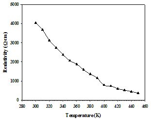 | Figure 5. Temperature dependent electrical resistivity of SnSe thin film with 500 nm thickness in the temperature range of 300 to 450 K |
3.4. Electrical Measurement
The temperature dependence of electrical measurement was carried out by the four-point probe method. The variation in the electrical resistivity of SnSe thin films of 500 nm thickness in the temperature range from 300 – 450 K is shown in Figure 5. The film was showing decrease in resistance with increase in temperature indicating semiconductor behaviour.The electrical resistivity of a polycrystalline thin film is a complex phenomenon, involving charge-carriers transport through the “bulk-like” part of the semiconductor crystals and inter-crystalline (grain) boundaries. The decrease in resistance with increase in temperature is due to increase in a) drift mobility of the charge carriers and b) free-carrier density (due to lattice vibrations). The temperature dependence of the semiconductor material’s resistivity is expressed by the Equation 5.Where, ρ is the resistivity (Ωcm), ρ0 is the pre-exponential factor, Ea is the activation energy for this thermally activated process, kb is the Boltzmann constant (8.617385 x 10⁻⁵ eV/K), and T is the corresponding temperature. The ln(ρ) versus 1000/T plot is shown in the Figure 6.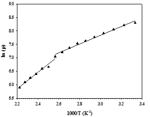 | Figure 6. Plot of ln(ρ) versus 1000/T for the SnSe thin film of 500 nm thickness |
A plot of ln(ρ) versus 1000/T would be a two straight line fitting in different temperature ranges, from the slope of it the activation energy (Ea) can be calculated. The values of activation energy found to be 0.14 eV for the 300-400 K temperature and 0.24 eV for the temperature range 400 - 450 K. From the Hot-Probe measurement, the polarity of the thermally generated voltage at the hot end being negative indicates p-type conductivity of the SnSe thin films.
4. Conclusions
Tin Selenide thin films have been successfully grown by thermal evaporation method on glass substrates held at room temperature with varying the film thicknesses from 150 nm to 500 nm. The structural analysis suggests that the thin films were polycrystalline in nature having preferred orientation in (111) direction. The surface roughness was apparently changed with increase in film thickness. The direct energy band gap calculated from the transmission data were in the range 1.74 to 1.24 eV. The electrical data shows that the SnSe thin film indicating semi-conducting behaviour with p-type conductivity. The narrow optical band gap (~1.3 eV) having p-type conductivity indicates its use in photovoltaic applications.
References
| [1] | C. R. Baxter and W. D. Mclennan, 1975, Ovonic type switching in tin selenide thin films, J. Vac. Sci. Technol., 12, 110-113. |
| [2] | N. R. Mathews, 2011, Electrodeposited tin selenide thin films for photovoltaic applications, Solar Energy, In press. |
| [3] | K. M. Chung, D. Wamwangi, M. Woda, M. Wuttig and W. Bensch, 2008, Investigation of SnSe, SnSe2, and Sn2Se3 alloys for phase change memory applications, J. Appl. Phys., 103, 083523 - 083529. |
| [4] | I. Lefebvre, M. A. Szymanski, J. Olivier-Fourcade, J. C. Jumas, 1998, Electronic structure of tin monochalcogenides from SnO to SnTe, Phys. Rev. B, 58(4), 1896-1906. |
| [5] | Z. Zainal, N. Saravanan, K. Anuar, M. Z. Hussein and W. M. M. Yunus, 2004, Chemical bath deposition of tin selenide thin films, Mater.Sci.Eng.B, 107(2), 181-185. |
| [6] | V. E. Drozd, I. O. Nikiforova, V. B. Bogevolnov, A. M. Yafyasov, E. O. Filatova and D. Papazoglou, 2009, ALD synthesis of SnSe layers and nanostructures, J.Phys. D, 42, 125306-125310. |
| [7] | D. P. Padiyan, A. Marikani and K. R. Murali, 2000, Electrical and photoelectrical properties of vacuum deposited SnSe thin films, Cryst.Res.Technol, 35(8), 949-957. |
| [8] | N. Kumar, V. Sharma, U. Parihar, R. Sachdeva, N. Padha and C. J. Panchal, 2011, Structure, optical and electrical characterization of Tin selenide thin films deposited at room temperature using thermal evaporation method, J. Nano- Electron. Phys., 3(1), 117-126. |
| [9] | J. P. Singh and R. K. Bedi, 1990, Tin selenide films grown by hot wall epitaxy, J. Appl. Phys., 68, 2776-2779. |
| [10] | G. H. Chandra, J. Naveen Kumara, N. M. Raob, and S. Uthanna, 2007, Preparation and characterization of flash evaporated tin selenide thin films, J. Cryst. Growth., 306, 68-74. |
| [11] | N. Kumar, V. Sharma, N. Padha, N. M. Shah, M. S. Desai, C. J. Panchal and I. Yu. Protsenko, 2010, Influence of the substrate temperature on the structural, optical, and electrical properties of tin selenide thin films deposited by thermal evaporation method, Cryst. Res. Technol., 45(1), 53-58. |
| [12] | Z. Zainal, N. Saravanan, K. Anuar, M. Z. Hussein and W. M. M. Yunus, 2003, Tin Selenide thin films prepared through combination of chemical precipitation and vacuum evaporation technique, Mater.Sci., 21(2), 225-233. |
| [13] | B. D. Cullity, 1956, Elements of X-ray diffraction, Addison-Wesley Publishing Co., Inc., Reading, Massachusetts. |
| [14] | G. K. Williamson and R. E. Smallman, 1956, III. Dislocation densities in some annealed and cold-worked metals from measurements on the X-ray Debye-Scherrer spectrum, Philos. Mag., 1(1), 34-45. |
| [15] | J. Tauc, 1974, Amorphous and liquid semiconductors, Chapter 4, ed. by J. Tauc, Plenum, London. |
| [16] | S. Sonmezoglu, A. Arslan, T. Serin and N. Serin, 2011, The effects of film thickness on the optical properties of TiO2–SnO2 compound thin films, Phys. Scr., 84(6), 065602-065607. |
| [17] | F. Urbach, 1953, The long-wavelength edge of photographic sensitivity and of the electronic absorption of solids, Physical Review, 92(5), 1324-1324. |
| [18] | S. Ilican, Y. Caglar and M. Caglar, 2008, Preparation and characterization of ZnO thin films deposited by sol-gel spin coating method, J. Optoelectron. Adv. Mater., 10(10), 2578-2583. |
 Abstract
 Reference
 Full-Text PDF
 Full-Text HTML