-
Paper Information
- Previous Paper
- Paper Submission
-
Journal Information
- About This Journal
- Editorial Board
- Current Issue
- Archive
- Author Guidelines
- Contact Us
American Journal of Materials Science
p-ISSN: 2162-9382 e-ISSN: 2162-8424
2011; 1(2): 149-153
doi: 10.5923/j.materials.20110102.25
Band Gap Determination of Copper Doped Tungsten Diselenide Single Crystals by Optical Absorption Method
 Abstract
 Reference
 Full-Text PDF
 Full-Text HTML
M. P. Deshpande , M. N. Parmar , Nilesh N. Pandya , Sandip V. Bhatt , Sunil Chaki
Department of Physics, Sardar Patel University, Vallabh Vidyangar, Gujarat, 388120, India
Correspondence to: Sunil Chaki , Department of Physics, Sardar Patel University, Vallabh Vidyangar, Gujarat, 388120, India.
| Email: |  |
Copyright © 2012 Scientific & Academic Publishing. All Rights Reserved.
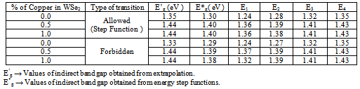
Absorption spectrum of copper (Cu) doped WSe2 (% of Cu = 0.0, 0.5, 1.0) single crystals were obtained in the range 700 nm to 1450 nm. The energy gap and phonon energies were determined for the crystals from the spectrum using two and three dimensional models. This study reflects that indirect transition is dominant in these crystals. On the basis of three dimensional models it was not possible for us to decide whether the indirect inter-band transition is forbidden or allowed type. Hence, different plots were made for two dimensional models, which showed that indirect forbidden transition holds accurately for this sample whereas indirect allowed type transition is not valid. The phonon energies calculated for these samples corresponds to the energies associated with optical phonons. The obtained results are discussed in details in this paper.
Keywords: Copper doped tungsten diselenide, Single crystals, Absorption coefficient, Bandgap
Cite this paper: M. P. Deshpande , M. N. Parmar , Nilesh N. Pandya , Sandip V. Bhatt , Sunil Chaki , "Band Gap Determination of Copper Doped Tungsten Diselenide Single Crystals by Optical Absorption Method", American Journal of Materials Science, Vol. 1 No. 2, 2011, pp. 149-153. doi: 10.5923/j.materials.20110102.25.
Article Outline
1. Introduction
- The layered transition metal dichalcogenides (TMDC’s) having general equation MX2 (M-transition metals like Mo, W, Zr, Nb, Ta, etc. and X – chalcogens like S, Se & Te) in single crystals and thin films form have been used in fabricating high efficiency solar cells, rechargeable batteries and high temperature solid lubricants[1-4]. The TMDC semiconductors are of interest in solar energy conversion due to the regular arrangement of structural lattice with cations and anions[1]. Of the TMDCs, WSe2 is a semiconductor with a bandgap in the range of 1.2 - 2 eV, depending on how the nonstoichiometry differs from the ideal W:Se ratio of 1:2[5]. The WSe2 is a black or gray color odorless material, possessing good thermal stability and a high melting point[6]. The high optical absorption, layered type of arrangement between cations, high resistance against photocorrosion and matching bandgap makes WSe2 a potential candidate for photoelectrochemical conversion and photovoltaic solar energy conversion. WSe2 has been used in a number of technologies such as high temperature solid lubrication and rechargeable batteries[7-8]. The WSe2 structure is characterized by a stacking of two-dimensional sandwich units (Se-W-Se) along the c-axis separated from each other by the so-called Van der Waals gap, the Se atoms forming the outer hexagonal dense planes[1]. The band gap of these materials plays an important role for its application hence it becomes necessary to determine it accurately.Herein, the authors report detailed study on determination of band gap of WSe2 single crystals having copper doped with three different percentage viz % of Cu = 0.0, 0.5, 1.0. The optical absorption technique was employed to determine the phonon energies and indirect transition in the crystals.
2. Experimental Methods
- The absorption spectra for the different concentration of Cu doped WSe2 (% of Cu = 0.0, 0.5, 1.0) single crystals were obtained using UV-VIS-NIR Shimadzu Spectrophotometer in the range 700 nm to 1450 nm as shown in Figure 1(a, b, c) respectively. Single crystals grown in thin flakes of approximately 0.35 m thickness were pasted on a thick black paper with a cut exposing the crystal flake to the incident light. The reference used is a replica of the black paper, having the cut in exactly the same position as the crystal flake.
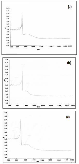 | Figure 1. Absorption spectra for copper doped WSe2 single crystals, % of Cu (a) 0.0 (b) 0.5 (c) 1.0 respectively |
3. Results and Discussion
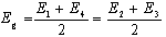
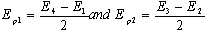
- In order to analyze the results from these spectra in the vicinity of the absorption edge, values of absorption coefficient ‘’ were determined at every step of 2.5 nm individually for all samples. Then these absorption spectra were analyzed on basis of already reported[9 - 11] three and two dimensional models. Figure 2 ( a, b, c ) and Figure 3 ( a, b, c ) shows the variation of the quantities (h)1/3 and (h)1/2 versus h for different % of Cu doped WSe2 (% of Cu = 0, 0.5, 1.0) single crystals respectively.
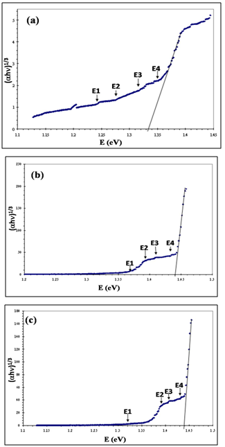 | Figure 2. (a, b, c) Plot of (h)1/3 versus E (eV) for different % of copper (Cu) doped WSe2 single crystals, % of Cu (a) 0.0 (b) 0.5 and (c) 1.0 respectively |
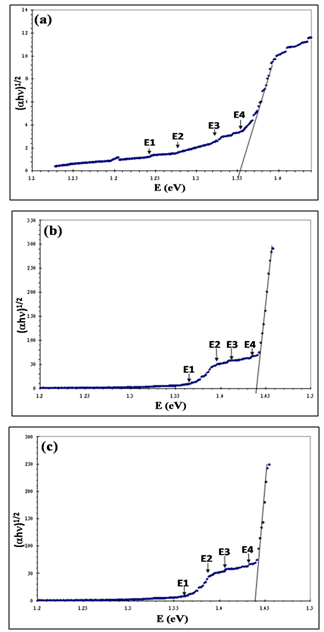 | Figure 3. (a, b, c) Plot of (h)1/2 versus E (eV) for different % of copper (Cu) doped WSe2 single crystals, % of Cu (a) 0.0 (b) 0.5 and (c) 1.0 respectively |
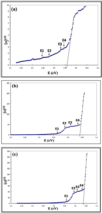 | Figure 4. (a, b, c) Plot of ()1/2 versus E (eV) for different % of copper (Cu) doped WSe2 single crystals, % of Cu (a) 0.0 (b) 0.5 and (c) 1.0 respectively |
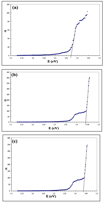 | Figure 5. (a, b, c) Plot of versus E (eV) for different % of copper (Cu) doped WSe2 single crystals, % of Cu (a) 0.0 (b) 0.5 and (c) 1.0 respectively |
 | (1) |
 | (2) |
|
|
4. Conclusions
- Determination of band gap by optical absorption method for Cu doped WSe2 (% of Cu = 0.0, 0.5 and 1.0 ) single crystals reflects that from three dimensional model it is difficult to predict whether the indirect transition is forbidden or allowed type whereas two dimensional model confirms the indirect transition to be forbidden type.
ACKNOWLEDGEMENTS
- All the authors are thankful to UGC, New Delhi for sanctioning DRS/SAP programme to the Department of Physics, Sardar Patel University which helped substantially to carry out this work.
References
| [1] | A. Aruchamy (Ed.), Photoelectrochemistry and Photovoltaics of Layered Semiconductors, Kulwer Academic Publishers, Dordrecht, 1992 |
| [2] | A. Ennaoui, K. Diesner, S. Fiechter, J. H. Mooser, F. Levy, Thin Solid Films, 1997, 311, 146 |
| [3] | S. Mary Delphine, M. Jayachandran, C. Sanjeeviraja, Mater. Chem. Phys., 2003, 81, 78 |
| [4] | M. Maret, B. Gilles, J. P. Simon, M. Verdier, I. Guhr, B. Riedlinger, M. Albrecht and G. Schatz, J. Cryst. Growth, 2005, 275, e2289 |
| [5] | Swati V. Pol, Vilas G. Pol, Jose M. Calderon-Moreno and Ahron Gedanden, J. Phys. Chem., 2008, C 112, 5356 |
| [6] | H. Haraldsen, Angew Chem. Inst. Ed., 1966, 5, 51 |
| [7] | A. H. Reshak and S. Auluck, Phys. Rev. B, 2003, 68, 195107 |
| [8] | T. Tsirlina, S. Cohen, H. Cohen, L. Sapir, M. Peisach, R. Tenne, A. Matthaus, S. Tiefenbacher, W. Jaegermann, E. A. Ponomarev, C. Levy-Clement, Sol. Energy Mater. Sol. Cells, 1996, 44, 457 |
| [9] | K Takahashi, T Arai and K Kudo, Sci. Light, 1972, 21,131 |
| [10] | V M Koshkin, V R Karas and LP Galchinetskii, Sov. Phys. Semicond., 1970, 3, 1186 |
| [11] | A M Elkorashy, J. Phys. Chem. Solids., 1986, 47,497 |
| [12] | A M Elkorashy, Proc. 14th Int. Conf. Phys. of Semiconductors, Edinburgh, 1978, 817 |
| [13] | A M Elkorashym, 7th Conference on Solid State Science , 15-18 April 1984, Military Technical College, Cairo , Egypt |
| [14] | C J Lewerenz, S D Ferris, C J Doharty and H J Leamy, J. Electrochem. Soc., 1982, 129, 418 |
| [15] | H Tributsch, Solar Energy Mater., 1979, 1, 257 |
| [16] | Jager-Waldau and E. Bucher, Thin Solid Films., 1991, 200, 157 |
| [17] | CR Cabrera and H D Abruna, J. Electrochem Soc., 1988, 135 (6), 1436 |
| [18] | S H El Mahalawy and B L Evans, Phys. Stat Sol (b), 1977, 79,713 |
| [19] | R Tenne and A Wold, Appl. Phys. Lett., 1985, 47(7), 707 |
| [20] | G Lucovsky, R M White, J A Benda and J F Revelli, Phys. Rev. B, 1973, 7, 3859 |
| [21] | J I Pankove, Optical Processes in Semiconductors, Prentice- Hall, Inc, Englewood Cliffs, New Jersey |