-
Paper Information
- Next Paper
- Previous Paper
- Paper Submission
-
Journal Information
- About This Journal
- Editorial Board
- Current Issue
- Archive
- Author Guidelines
- Contact Us
American Journal of Materials Science
p-ISSN: 2162-9382 e-ISSN: 2162-8424
2011; 1(1): 45-51
doi: 10.5923/j.materials.20110101.07
Ab initio Calculations of Structural and Electronic Properties of the III-V Nitride Compounds and their Applications to Laser Diodes
 Abstract
 Reference
 Full-Text PDF
 Full-Text HTML
Abbès Beloufa 1, Zouaoui Bensaad 1, Bel-Abbes Soudini 1, Nadir Sekkal 2, Abdellah Bensaad 1, Hamza Abid 1
1University of Sidi Bel Abbès, 22000 Sidi Bel Abbès, Algeria
2Département de Physique-Chimie, ENST, BP 1523, El M’Naouer, 31000 Oran, Algeria
Correspondence to: Abbès Beloufa , University of Sidi Bel Abbès, 22000 Sidi Bel Abbès, Algeria.
| Email: |  |
Copyright © 2012 Scientific & Academic Publishing. All Rights Reserved.
This paper reports the first-principles calculations of the electronic and the structural properties of AlN, GaN, InN, AlGaN and InGaN in various crystal structures. The computational method used to investigate the structural and the electronic properties is the full potential linear muffin-tin orbital (FP-LMTO) augmented by a plane-wave basis (PLW). Exchange-correlation has been accounted for within LDA using the exchange-correlation potential calculated by Vosko et al. and Perdew et al. The latter parameterisation takes into consideration the generalized gradient approximation (GGA). The results of the calculated properties for the considered compounds in the zincblende and wurtzite phases are discussed and compared to the theoretical works as well as to the experimental data. We have also applied this computational method to AlGaN and InGaN alloys to check its transferability to predict the structural and electronic properties from those of their parent compounds. As an example, we have interested to the heterojunction based on the studied compounds. So, we have presented the theoretical analysis of the gain characteristics of InGaN/AlGaN quantum dot (DL) laser. The results obtained confirm the powerful of the method used for the calculation on the one hand, and in the other hand, the III-V nitride compounds and their alloys are potential candidates for new generation of light emitters likes the lasers diode.
Keywords: Electrical Properties, Structural Properties, (In, Al, Ga)N, Gain, Lasers Diodes, LMTO Methods
Cite this paper: Abbès Beloufa , Zouaoui Bensaad , Bel-Abbes Soudini , Nadir Sekkal , Abdellah Bensaad , Hamza Abid , "Ab initio Calculations of Structural and Electronic Properties of the III-V Nitride Compounds and their Applications to Laser Diodes", American Journal of Materials Science, Vol. 1 No. 1, 2011, pp. 45-51. doi: 10.5923/j.materials.20110101.07.
Article Outline
1. Introduction
- There is a growing interest in the study of the III-V Nitride compounds (GaN, InN, A1N and their alloys) due to their technological importance. Particularly, these materials are potential candidates for new generation of light emitters and other optoelectronic devices operating across the visible and UV wavelengths, and most studied of wide bandgap semiconductors have been the III-nitrides. Among them, GaN and its alloys with InN and AIN have attracted great attention since the successful commercialization of bright blue/green light-emitting diodes followed later by the demonstration of injection lasers[1,2]. Researchers considered the III nitrides to be laboratory curiosities, unlikely to be of great practical importance. However, after several breakthroughs in growth and doping technologies, the III nitrides have emerged as the leading semiconductor materials for short-wavelength (green, blue, and violet) visible-light-emitting diodes and laser diodes, as well as solar-blind photodetectors, and show promise for high-power, high-frequency, and high-temperature microelectronics. There are many theoretical studies reported elsewhere for GaN[3,4], for InN[3,5], for AlN[6,7], for InGaN[8,9] and for AlGaN[10,11]. Major developments in wide-gap III–V nitride semiconductors have recently led to the commercial production of high-brightness blue/green light-emitting diodes (LED’s)[12] and to the demonstration of room-temperature (RT) bluish-purple laser light emission in InGaN–GaN–AlGaN-based heterostructures under pulsed currents[13,14] and continuous-wave (CW) operation[15, 16]. These developments are a result of the realization of high quality crystals of AlGaN and InGaN, and p-type conduction in AlGaN[17,18]. The recombination of localized excitons has been proposed as an emission mechanism for this InGaN quantum-well-structure LED’s[19].In an attempt to give a more systematic understanding of the structural and the electronic properties of these Group-III nitrides and their related alloys, we have carried out our calculations within the local density approximation (LDA) to density functional theory, using the all-electron full potential linear muffin-tin orbital (FP-LMTO) augmented by a plane-wave basis (PLW). The exchange- correlation energy of electrons is described in the local density approximation (LDA) using the parameterization of Vosko et al.[20] and also of Perdew et al.[21]. We have also applied this computational method to AlGaN and InGaN systems greatly used in the heterostructures and the quantum wells to check its transferability to predict the structural and electronic properties from those of their parent compounds.
2. Method of Calculation
- The full-potential linear muffin-tin (FP-LMTO) method is a specific implementation of density functional theory within the local density approximation (LDA). In this method there is no shape approximation to the crystal potential, unlike methods based on the atomic-spheres approximation (ASA) where the potential is assumed to be spherically symmetric around each atom. For mathematical convenience, the crystal is divided up into regions inside muffin-tin spheres, where Schrödinger’s equation is solved numerically, and an interstitial region. In all LMTO methods the wave functions in the interstitial region are Hankel functions. Each basis function consists of a numerical solution inside a muffin-tin sphere matched with value and slope to a Hankel function tail at the sphere boundary. The so-called multiple –kappa basis is composed of two or three sets of s, p, d, etc. LMTO’s per atom. The extra variational degrees of freedom provided by this larger basis allow for an accurate treatment of the potential in the interstitial region.In the present work, we use the Savrasov version of the full potential linear muffin-tin orbital (FP-LMTO) method augmented with a plane wave basis (PLW)[22]. The non overlapping muffin tin spheres potential is expanded in spherical harmonics inside the spheres and Fourier transformed in the interstitial regions. The exchange-correlation energy of electrons is described in the local density approximation (LDA) using the parameterization of Vosko et al. and also of Perdew et al.[21].It is a well-known that the LDA has a tendency to overestimate the bonding. The improvement by the GGA is in fact mainly due to an improvement in the calculation of the atomic reference energies. Since the free atoms contain regions of very low density and strongly varying electronic density, gradient corrections to the exchange and correlation functional are more important for free atoms than for bulk. The lattice constant is usually underestimated with respect to the experimental lattice constant by up to a few percent by the LDA while the GGA sometimes overestimates it. In this work, the orbital 3d10, 4s2, 4p1 of Ga, 4d10, 5s2, 5p1 of In, 2s2, 2p3 of N, and 3s2, 3p1 of Al are all included into the self-consistent treatment, i.e. viewed as valence electrons. The present calculation methods are implemented in the available computer code lmtART[23]. Basis functions, charge density, and potential were expanded inside the muffin-tin spheres in spherical harmonic functions with cut-off
 , and in Fourier series in the interstitial region. In the muffin-tin spheres (MTS) of radius RMT, the upper limit on the angular momentum expansion of the smoothed Hankel functions about a given atomic site is carried out up to
  [24].
[24]. for the wurtzite phase for which the volume per unit formula is taken into account. Both FPLMTO results is presented.
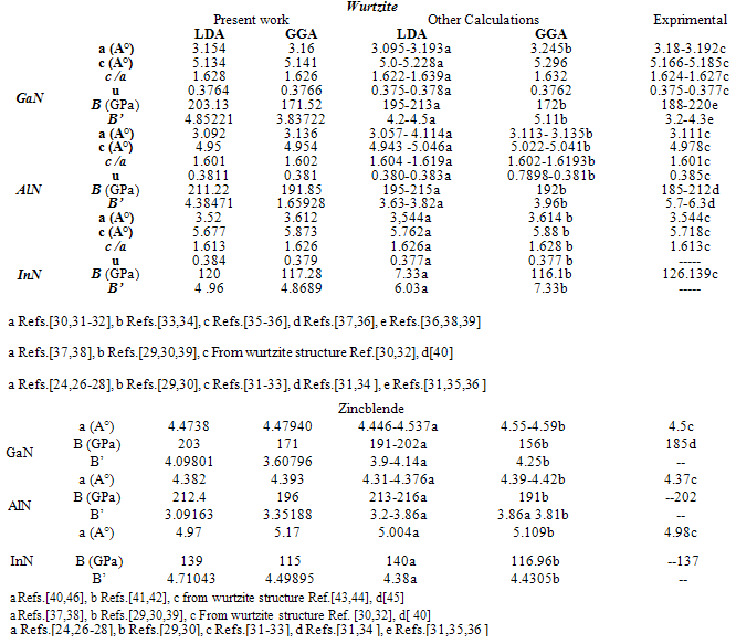
3. Results and Discussions
- The total energy versus volume for GaN, AlN and InN in both the zincblende (8 atoms) and the wurtzite structures (16 atoms) was calculated in our previous work[24]. Let us discuss now the results of the band structure calculation. The static properties of the phase under study (equilibrium lattice constant, bulk modulus, and its pressure derivative) for the studied compounds are determined using the Murnaghan/Birch equation of state to fit our calculated E-V data. The results compared to experiment and other works are given in Table 1.In Fig. 1, the band structure of these materials in the Zincblende (B1) phase for the equilibrium volume is shown. The band structure of InN shows a direct band gap at Γ, closely similar to that of GaN. This is very different from what we have found for AlN, where we notice a small indirect Γ–X fundamental band gap. Our calculated band gaps obtained with the LDA for the zincblende form are Eg=3.33eV, Eg=0.6eV and Eg=5.76 eV for GaN, InN and AlN, respectively. These values are in good agreement compared to the experimental bands gaps found by M. Marques et al.[25] (3.3 eV for GaN, 0. 9 eV for InN and 5.94 eV for AlN) and those of Munoz et al.[26]. However, these band gaps are underestimated by other theoretical works as PWPP method and the FP-LAPW method[27]. It is well known that in the wurtzite case of GaN and AlN, the lowest conduction band and the top of the valence bands are situated at the Γ point in the BZ. Without spin-orbit interaction they are related to an s-like Γ1c state and to p-like Γ6v and Γ1v states. The two latter states are separated by a crystal-field splitting
 . Two energy gaps can be defined by
  and
and  according to the optical transition
  and
and  . In GaN,
  is the fundamental gap, whereas in AlN it is the C transition gap due to the negative crystal field splitting[28,29].In order to characterize the optical gain and the threshold current density of laser diodes for different temperatures (transparency density) and cavity length in our laser structures, we have calculated the energy bandgaps and the refractive index. Optimization of intrinsic and extrinsic parameters such that: absorption coefficient (α), electronic affinity (χ), confinement factor (Γ) and effective mass, represents the principle stage in the design of a laser diode. These optimized parameters are obtained using the combined LMTO method, Mathematica and Mathcad calculations. The first structure studied is the simple heterostructure based on the studied compounds. Above this transparency threshold, the medium begins to amplify those photons possessing energies which satisfy the Bernard—Durrafourg condition. The gain spectrum is then given by:
 | (1) |
 is the gain of the semiconductor medium
  is the empty conduction band absorption (i.e. under zero current) with[43]:
 | (2) |
 and
and  are the occupation rates for the levels in the conduction and valence bands satisfying
  .
. | Figure 1. The band structure of GaN, InN, AlN, InGaN and AlGaN in the equilibrium phase for the equilibrium volume. |
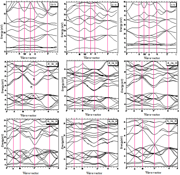
 | Figure 2. Evolution of the quasi-Fermi level difference as a function of non-equilibrium carrier density in InGaN. |
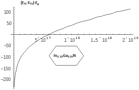
 | Figure 3. Evolution of the gain curve maximum in InGaN as a function of electron-hole pair density. |
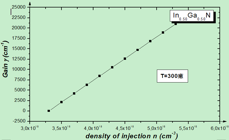
 will lasing) shows a linear increase with the density of carriers to the above of the threshold of transparency. In Fig. 4, we have illustrated the evolution of the gain according to the energy of the photons for various densities of injection in the two materials (GaN and In0.5Ga0.5N). Once transparency has been achieved, the maximum gain increases linearly with charge density above threshold. This purely phenomenological relationship is very useful in modelling the behaviour of semiconductor lasers.
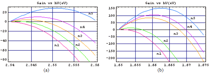 | Figure 4. Evolution of the Gain according to the energy of the photons for various densities of injection in the two materials (a) GaN, (b) (In0.5Ga0.5N). |
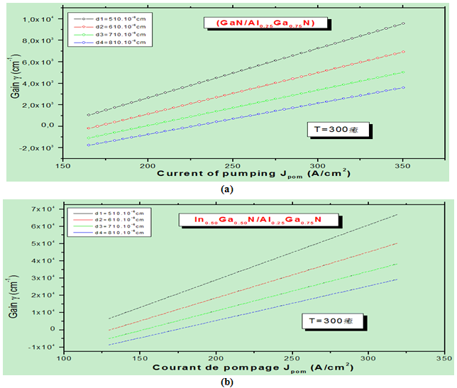 | Figure 5. Evolution of the maximum Gain according to the current of pumping for various values thickness of the two materials (a) GaN, (b) (In0.5Ga0.5N). |
4. Laser Diode with Double Heterojunction
- To improve the laser diode performances, we must increase the Gain with the minimization of the current. Then we have studied the second structure where the confinement factor plays an important role for satisfying the above condition. From the studied compounds, we have considered the double heterostructure (DH) where at the first stage we started by determining certain sizes characteristic as the losses (parasitic losses which come from the free carriers of the electrical contacts of the diffusion and the losses intrinsic that corresponds to the escape of the photons) for a fixed width of 600 A°. Fig. 5 shows that the Gain increases when the current of pumping decreases in the case of a structure with double heterojunction for two materials with various thicknesses of the cavity. By comparing the variation of the threshold in the DH laser diode type with DH with that of in an heterojunction diode, one observes a difference in the current of threshold (returns decreased the thickness of the cavity of some micrometers) which comes from the weak optical confinement on the one hand, and on the other hand from the lower volume to reverse in an heterojunction. The value of 0.1 μm structural features DH is comparable with the optical wavelengths and consequently allows an optimised confinement of photons. On the other hand, this value is much higher than the electronic wavelengths, so that the confinement of electrons can be improved considerably. It is the role of the quantum well[47-49].
5. Conclusions
- Our calculated lattice parameter is found to be in reasonable agreement with other theoretical works as well as the experimental result. From the E-V curves, we found that for the studied compounds, the wurtzite form is slightly lower in energy than that of the zincblende form. Hence, for the low pressure, these compounds show the new equilibrium phase which is the zincblende structure. At high pressure, we can predict that the new phase is probably the rock salt structure. We have also applied this computational method to AlGaN and InGaN alloys to check its transferability to predict the structural and electronic properties from those of their parent compounds. As a function of composition, the alloys of GaN and InN should cover the entire spectral region from the very near UV to the red while AlGaN covers a wide range in the near UV. We notice that most significant in all this study, is the remarkable quantitative difference found between the two systems studied in this article, i.e., GaN\Al0.25Ga0.75N and In0.5Ga0.5N\Al0.25Ga0.75N. Finally, one can state that the use of a laser diode containing the In0.5Ga0.5N\Al0.25Ga0.75N\GaN structure leads to better performances. The results presented in this work were considered as a contribution to the current state of the art, in the development of the lasers diode with double heterojunction. We can say that the laser diode remains a very active subject of research. The works in progress continue to extend their applicability while improving their performance such as for example the spectroscopies for detection of pollution. The difficulties occur when one seeks to join together several extreme characteristics unit[46].
References
| [1] | S. Nakamura, T. Mokai, M. Senoh, Jpn. Appl. Phys. 30 (1991) 1998 |
| [2] | S. Nakamura, T. Mokia, M. Senoh, Appl. Phys. Lett. 64 (1994)1687 |
| [3] | A. Sher, M. van Schilfgaarde, M. A. Berding, S. Krishnamurthy, and A.-B. Chen, MRS Internet J. Nitride Semicond. Res. 4S1, G5.1 (1999) |
| [4] | A. Qteish , A.I. Al-Sharif , M. Fuchs , M. Scheffler , S. Boeck , J. Neugebauer, Computer Physics Communications 28–31, (2005) 169 |
| [5] | T.V. Shubina, Phys. Rev. Lett. 92, (2004) 117407 |
| [6] | A. Kobayashi, O. F. Sankey, S. M. Volz and J. D. Dow, Phys. Rev. B28, (1983) 935 |
| [7] | P. E. Van Camp, V. E. Van Doren and J. T. Devreese, Phys. Rev. B44, (1991) 9056 |
| [8] | Kwiseon Kim, Ph.D. thesis 1998, Case Western Reserve University, unpublished. |
| [9] | Y. K. Kuo, and B-T Liou, S. H. Yen, and H. Y. Chu Opt. Commun. 237 (2004) 363-9 |
| [10] | A. Rubio, J. L. Corkill, and M. L. Cohen, Phys. Rev. B 49, (1994) 1952 |
| [11] | Z. Dridi, B. Bouhafs, P. Ruterana, Comput. Mater. Sci. 33 (2005) 136-40 |
| [12] | S. Nakamura, M. Senoh, N. Iwasa, S. Nagahama, T. Yamada, and T. Mukai, Jpn. J. Appl. Phys. Lett., vol. 34, (1995) pp. L1332–L1335 |
| [13] | S. Nakamura, M. Senoh, S. Nagahama, N. Iwasa, T. Yamada, T. Matsushita, H. Kiyoku, and Y. Sugimoto, Jpn. J. Appl. Phys., vol. 35, (1996) pp. L74–L76 |
| [14] | K. Itaya, M. Onomura, J. Nishino, L. Sugiura, S. Saito, M. Suzuki, J. Rennie, S. Nunoue, M. Yamamoto, H. Fujimoto, Y. Kokubun, Y. Ohba, G. Hatakoshi, and M. Ishikawa, Jpn. J. Appl. Phys., vol. 35, (1996) pp. L1315–L1317 |
| [15] | S. Nakamura, M. Senoh, S. Nagahama, N. Iwasa, T. Yamada, T. Matsushita, Y. Sugimoto, and H. Kiyoku, Appl. Phys. Lett., vol. 69, (1996) pp. 3034–3036 |
| [16] | S. Nakamura, M. Senoh, S. Nagahama, N. Iwasa, T. Yamada, T. Matsushita, Y. Sugimoto, and H. Kiyoku, Appl. Phys. Lett., vol. 69, (1996) pp. 4056–4058 |
| [17] | S. Strite and H. Morko¸c, J. Vac. Sci. Technol., vol. B10, (1992) pp. 1237–1266 |
| [18] | M. A. Khan, J. N. Kuznia, A. R. Bhattarai, and D. T. Olson, Appl. Phys. Lett., vol. 62, (1993) pp. 1786–1788 |
| [19] | S. Chichibu, T. Azuhata, T. Sota, and S. Nakamura, Appl. Phys. Lett., vol. 69, (1996) pp. 4188–4190 |
| [20] | S.H.Vosko, L.Wilk and M. Nussair, Can. J. Phys. 58 (1980)1200 |
| [21] | J. P. Perdew, S. Burke, M. Ernzerhof, Phys. Rev. Lett. 77 (1996) 3865 |
| [22] | S. Y. Savrasov, Phys Rev B 54 (1996) 16470 |
| [23] | http://www.physics.ucdavis.edu/∼mindlab/Orbitals, Vienna University of Technology, Vienna, Austria, (2001) |
| [24] | A. Beloufa,, Z. Bensaad, B. Soudini, N. Sekkal, A. Bensaad, H. Abid, Int. J. Nanoelectronics and Materials 2 No. 1 (2009). 11-22 |
| [25] | M. Marques, L. K. Teles, L. M. R. Scolfaro, and J. R. Leite, Appl. Phys. Lett. 83 (2003) 890 |
| [26] | A. Munoz, K. Kunc, Physica B 185 (1993) 422 |
| [27] | S. Berrah, H. Abid and A. Boukortt, Phys. Scr. 74 (2006)104-107 |
| [28] | H. Yampashita, K. Fukui, S. Misawa, and S. Yodhida, J. Appl. Phys. 50, 896 (1979) |
| [29] | A. Rubio, J. L. Corkill, M.L. Cohen, E.L. Shirley, and S.G. Louie, Phys. Rev. B 48, 11 810 (1993) |
| [30] | J. Serrano, A Rubio, E. Hernandez, A. Munoz and A. Mujica, Phys. Rev. B 62 (2000) 16612 |
| [31] | I. Vurgaftmana and J. R. Meyer L. R. Ram-Mohan, J. Appl. Phys. 89 (2001) 5815 |
| [32] | K. Kim, W. R. L. Lambrecht, and B. Segall, Phys. Rev. B 50 (1994) 1502 |
| [33] | V.I. Gavrilenko and R.Q. Wu, Phys. Rev. B 61 (2000) 2632 |
| [34] | C.-Y. Yeh, Z. W. Lu, S. Froyen, and A. Zunger, Phys. Rev. B 46 (1992) 10 086 |
| [35] | M. Ueno, M. Yoshida, A. Onodera, O Shimomura and K. Takemura, Phys. Rev. B49 14(1994) |
| [36] | Properties of Group III Nitrides, edited by J.H. Edgar, Electronic Materials Information Service (EMIS) Datareviews Series (Institution of Electrical Engineers, London, (1994) |
| [37] | V.I. Gavrilenko and R.Q. Wu, Phys. Rev. B 61(2000) 2632 |
| [38] | C.-Y. Yeh, Z. W. Lu, S. Froyen, and A. Zunger, Phys. Rev. B 46 (1992) 10 086 |
| [39] | P. Perlin, C. Jauberthie -Carillon, Lti, A.S. Miguel, I. Grzegory, A. Polian, High Press. Res. 7 (1991) 96 |
| [40] | M. Abu-Jafara, A.I. Al-Sharif, A. Qteish, Solid Stat. Comm. 116 (2000) 389 |
| [41] | I. Vurgaftmana and J. R. Meyer L. R. Ram-Mohan, J. Appl. Phys. 89 (2001) 5815 |
| [42] | Q. Xia, H. Xia, and A.L. Ruoff, J. Appl. Phys. 73, 8198 (1993) |
| [43] | A. Munoz, K. Kunc, Physica B 185 (1993) 422 |
| [44] | M.E. Sherwin and T.J. Drummond, J. Appl. Phys. 69 (1991) 8423 |
| [45] | A. Trampert, O. Brandt and K.H. ploog, in Crystal Structure of Group III Nitrides, Edited by J.I. Pankove and T.D. Moustakas, Semiconductors and Semimetals Vol. 50 (Academic, San Diogo (1998) |
| [46] | E. Rossencher, optoélectronique (1998) |
| [47] | H. Ohta, S. P. DenBaars, and S. Nakamura, J. Opt. Soc. Am. B 27(2010) B45-B49 |
| [48] | T. K. Sharma and E. Towe m Appl. Phys. Lett. 96 (2010) 191105 |
| [49] | W. G. Scheibenzuber, C. Hornuss and U. T. Schwarz, , Proc. of SPIE 7953, 79530K (2011) |