-
Paper Information
- Next Paper
- Previous Paper
- Paper Submission
-
Journal Information
- About This Journal
- Editorial Board
- Current Issue
- Archive
- Author Guidelines
- Contact Us
American Journal of Materials Science
p-ISSN: 2162-9382 e-ISSN: 2162-8424
2011; 1(1): 12-17
doi: 10.5923/j.materials.20110101.03
On the Conduction Mechanism of Silicate Glass Doped by Oxide Compounds of Ruthenium (Thick Film Resistors). 2. Nanocrystals in the Glass and Charge Carrier's Localization
 Abstract
 Reference
 Full-Text PDF
 Full-Text HTML
G. Abdurakhmanov
Institute of Power Engineering and Automation, the Uzbek Academy of Sciences, 29 Do’rmon yo’li, Tashkent, 100125, Uzbekistan
Correspondence to: G. Abdurakhmanov , Institute of Power Engineering and Automation, the Uzbek Academy of Sciences, 29 Do’rmon yo’li, Tashkent, 100125, Uzbekistan.
| Email: |  |
Copyright © 2012 Scientific & Academic Publishing. All Rights Reserved.
Conduction mechanism of doped silicate glasses based on existence of nanocrystals is proposed. These nanocrystals are effective centers of localization of free charge carriers, and variable range hopping of last ones takes place. It is shown that dopant atoms generate narrow impurity subband of about 0,03 eV in width, which is slightly (less than 0.01 eV) separated from the top of the valence band of the glass or abutted on them, so thermal activation coexists with hopping conduction. Because of it the resistivity of the doped silicate glass is proportional to exp(-aT-ζ) at low temperatures (T < 50 K), 0.4 < ζ < 0.8. Structural transitions of nanocrystals take place at high temperatures (T > 800 K) and the conductivity of the doped silicate glass decreases sharply. Beyond the conductivity minimum (above 1000 K) the impurity subband and the top of the valence band of glass are separated by energy gap of 0.05 – 1.5 eV in width, so doped silicate glass behaves like a typical semiconductor.
Keywords: Lead-silicate Glass, Thick Film Resistors, Doping and Percolation Levels, Nanocrystals, Localization and Hopping of Charge Carriers, Impurity Subband and Thermal Activation, Conductivity, Firing Conditions
Cite this paper: G. Abdurakhmanov , "On the Conduction Mechanism of Silicate Glass Doped by Oxide Compounds of Ruthenium (Thick Film Resistors). 2. Nanocrystals in the Glass and Charge Carrier's Localization", American Journal of Materials Science, Vol. 1 No. 1, 2011, pp. 12-17. doi: 10.5923/j.materials.20110101.03.
Article Outline
1. Introduction
- We have reported earlier[1] on the transport properties of the doped silicate glass (DSG, better known as the thick film resistors), determined by diffusion of the dopant atoms into the glass and formation of diffusion zones. These processes leads to the formation of the percolation levels for free charge carriers in the glass, and can explain the effects of the dopant content, firing conditions and dispersivity of dopant powder on conductivity σ of the DSG. There are number of investigations on the conduction mechanism of the DSG[2-6] where the interaction of the glass and the conductive phase has been declared. A detailed study of the influence of various experimental parameters (temperature, RuO2 content, stirring, etc.) on the electrical conductivity and, in particular, on the percolation threshold in borosilicate glass–RuO2 composites is presented in[2]. This percolation threshold is shown to increase by a factor of two (from 0.6 to 1.2 vol%) when stirring is applied during synthesis and by more than a factor of three (>2.1 vol%) when a sol–gel route is used. Besides,the study of various synthesis temperatures reveals that the electronic part of the electrical conductivity is highly correlated to Ru solubility in the glass matrix. It was concluded from these experiments that both the presence of dissolved ruthenium in the glass matrix and the possibility of RuO2 particles to rearrange in the melt in order to form kind of a network are necessary for a low percolation threshold. The last conclusion is erroneous because of the considerable deviations of resistivity values of samples estimated for such network of RuO2 particles and measured experimentally for same volume content of RuO2. Jagtap et all[3] have added some compounds into the thick film composite (glass+conductive phase) to reduce the temperature coefficient of resistivity, but the mechanism of this effect did not explained. Low frequency noise spectroscopy is employed in[4] to examine fluctuating phenomena that take place in the material of resistive films and in the film/termination interface of a thick-film resistor. It has been found that the excess low frequency noise apart from the 1/f component contains contributions from thermally activated noise sources with energies in the range 0.015–0.6 eV. These sources are considered to be distributed nonuniformly over the whole resistor volume, most probably in the glassy matrix or conductive grain boundaries.It was confirmed[5] that the diffusion of ruthenium into glass affects the binding state of RuO2 at the interface of the glass. Furthermore, an intermediate resistive layer is detected around the RuO2 particle. These results suggest that the piezoresistive effect is related to a change in the electrical conductivity of the interfacial reaction layer caused by the diffusion of ruthenium into glass.Noise properties of thick-film resistors of various compositions have been investigated in[6] and conclusions concerning compatibility of resistive and conductive pastes have been formulated. Unfortunately, in all these works as well as in earlier investigations[7, 8] suggested interactions of the glass and the conductive phase (mainly RuO2) were not summarized into the detailed conduction model of the DSG and the effect of nanoscale glass structure on the conductivity of DSG was not considered.The conduction mechanism of DSG as the result of its nanoscale structure is investigated in the present paper.Direct and doubtless evidences of the existence of nanocrystals (or microcrystallits, as they have been called earlier) in the glass are not found yet. That is why the problem of the glass structure (continuous random network, Zachariasen, 1932; microcrystallits, separated by interlayer of disordered atoms, Lebedev, 1921) is still a subject of discussion. But temperature dependence of some glass properties such as viscosity, thermal expansion coefficient, dielectric constant and dielectric loss, have anomalies which have a better agreement with microcrystalline theory. This is especially the case for many-component glasses. One should take into account that these nanocrystals are not detected by X-ray diffraction method because of their small size (about 1 – 2 nm). At the same time structure and properties of these nanocrystals can differ essentially from that of the bulk. The last fact can be clearly traced during the milling process of various materials up to submicron size.The doping process used here is standard for technology of thick film resistors and was described elsewhere (the mixture of the glass and the dopant powders have been fired at Tf = 1125 K in τ = 10 min). Content of RuO2 in our samples of doped glass was 16, 20 and 30 weight %. The lead-silicate glasses investigated have the following composition (weight %): Glass1SiO2 – 33; PbO – 67; Glass2SiO2 – 27; PbO – 67; BaO – 4; MgO – 2.
2. Nanocrystals in the Glass and Localization of Charge Carriers
- Metastability of glassy state is widely accepted[9] and all kinds of glasses will become crystalline with time. The time required for this transition may be many years or even millennium depending on its composition and thermal prehistory, i. e. depending on the height of potential barrier, separating these two states. are formed spontaneously in the glass so the Helmholtz energy of the crystalline state is lower than that of the glassy state of same composition. It means that these crystals act as pockets of potential energy. The silicate glass is dielectric with energy gap as high as 3.3 - 7 eV (the glass 2SiO2·PbO and fused silica accordingly). On the other hand natural crystallization of the silicate glass is very slow (usually tens of years), and relevant energy of this process is insignificant. Because of this one can assume that the pockets are not deep (of about 0.01 – 0.03 eV) and dynamical balance of transitions from glassy state into crystalline state and back is slightly disturbed in the line of first.Free charge carriers in DSG are holes as it is indicated by the sign of the thermopower[10]. Concentration of them is about 1020 cm-3 and the effective mass m* is about 330 m0 (m0 is mass of the free electron) as it was estimated from the resistivity ρ and the upper limit of mobility μ of DSG[11]. The increase of effective mass of electrons (holes) in the small size pockets have been demonstrated in[12] for GaN.The bottom of the conduction band of the lead-silicate glass is formed by the shifted 3s-orbitals of the oxygen and 6d-orbitals of the lead, while the top of the valence band is formed by shifted 2p-orbitals of O2 and 6p-orbitals of Pb[13]. As a result, lead-silicate glass is the dielectric with the band gap about 3.3 eV[14], and the silica glass has Eg ≈ 7.76 eV[15], since the conduction and valence bands are formed by shifted 3s- and 2p-orbitals of O accordingly. Doping of the lead-silicate glass forms the impurity subband from shifted 5s-states of Ru atoms. 6p-states of Pb and 5s-states of Ru are shifted to 7.415 eV and 7.36 eV below the vacuum level (first ionization potential,[16]) accordingly. It is known that conductivity of DSG varies very slowly in the wide temperature range and the photoconductivity do not appears up to the ultraviolet, where transition of electrons from the valence band into the conduction band takes place. So one can say that ruthenium subband abutted to top of the valence band of glass or slightly (less than 0.01 eV) separated from the last (Figure 1a). Then the Fermi level EF appears as close to the top of the valence band as 0.01 eV or less and the gas of free carriers is degenerated at room temperature.This is confirmed by infrared (IR) and optical spectra of DSG (Figure 2 and 3). μ is absorbance (arbitrary units), λ and
 are wavelength and wave number accordingly in these spectra. We assume that the arms at 50 μm (hν ≈ 0.026 eV) and at 12 μm (hν ≈ 0.1 eV) on the IR-spectrum of DSG (Figure 2, curve 4) correspond to the electron transitions from the glass valence band into the impurity subband because they are not characteristic neither of glass (Figure 2, curve 1) nor of RuO2 (Figure 2, curve 2), and shoulder at 12 μm can be caused by transitions from the pockets generated by nanocrystals into the subband (Figure 4). So one can estimate the depth of the pockets as 0.1 – 0.025 = 0.075 eV.
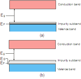 | Figure 1. Energy bands in DSG at T < 700 K (a) and at T > 700 K (b) |
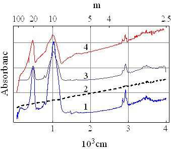 | Figure 2. IR-spectra of the glass1 (1), RuO2 (2), unfired mixture of them (3) and DSG (4) |
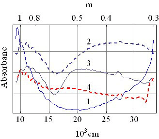 | Figure 3. Optical spectra of the glass1 (1), RuO2 (2), unfired mixture of them (3) and DSG (4) |
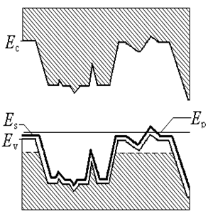 | Figure 4. Energy pockets of nanocrystals in the glass, impurity subband and the regions of free carriers localization. Ec and Ev are the conductivity and the valence bands of the glass accordingly, Es is the impurity subband, Ep is the percolation level |
3. Concentration of the Free Charge Carriers, IR- and Optical Spectra
- The IR-spectrum of RuO2 powder (Figure 2, curve 2) is the most curious one, where the absorbance decreases monotonically without appearance of any noticeable bands as the wavelength increases. Such spectrum is typical for absorption of the electromagnet waves by free charge carriers in the plasma resonance region[17]. This means that the concentration of free carriers in RuO2 powder is high and absorption on them suppresses the molecular absorption[18]. IR-spectrum of the DSG in the 2.5 – 7 μm range on repeats the IR-spectrum of RuO2, i.e. the concentration of free carriers in DSG is high enough, although the molecular absorption bands of higher intensity at 10 and 20 μm (intrinsic vibrations of the[SiO4]-tetrahedra) are still visible.Optical spectra (Figure 3) show that all the characteristic absorption bands of the glass (curve 1) and the RuO2 (curve 2) disappear in the DSG (curve 4) while in the spectrum of unfired mixture of these powders (curve 3) they are clearly seen.These spectra confirm that there are no deep energy levels in the energy gap of the glass and absorption starts beyond the 0.3 μm where interband transitions of the glass take place (we have not taken into account there the impurity subband because of its small width and displacement close to top of the valence band). Impurity subband formation close to the top of the glass valence band (acceptor states) was pointed out in[19].This implies that all the states in the impurity subband are ionized at room temperature and conductivity of DSG does not vary substantially with the temperature.
4. Temperature Dependence of Conductivity of the DSG
- Coexistence of glassy and crystalline sections (and potential energy pockets as accordingly) in DSG as well as narrowness of the impurity subband and its proximity to the top of the glass valence band leads to the following:1) All the states in the impurity subband are ionized at room temperature, gas of carriers is degenerated and the temperature dependence of the conductivity of DSG σ(T) is very weak.2) Particularly, at low temperatures when the impurity states are ionized, the simultaneous action of the activation and hopping mechanisms of conductivity in DSG is possible, so the total conductivity is where the first term corresponds to the activation mechanism with the activation energy Eg(T) and the second term corresponds to the variable range hopping (Mott’s low[20]). A and B are constants depending on the relative volumes of glassy and nanocrystalline sections, k is the Boltzmann’s constant, T0 is the temperature constant (T0 ~ 106 K). The temperature dependence of the activation energy is given as[21]
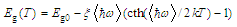 | (2) |
 is an average phonon energy.The equation (1) can be fairly well approximated by
 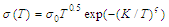 | (3) |
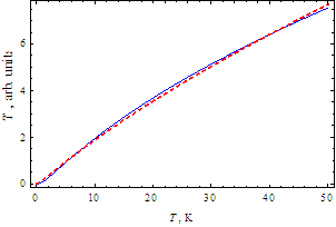 | Figure 5. Temperature dependence of the DSG conductivity – comparison of expressions (1) (dotted line) and (3) (solid line) at: A = 1040; B = 3.5; T0 = 100 К; Eσ0 = 10-2 эВ; ξ = 1.1;  K; σ0 = 1.67; K = 10 K; ς = 0,5. K; σ0 = 1.67; K = 10 K; ς = 0,5. |
 | Figure 6. Temperature dependence of the resistance R and the thermopower S of DSG based on the glass1 (a) and glass2 (b). |
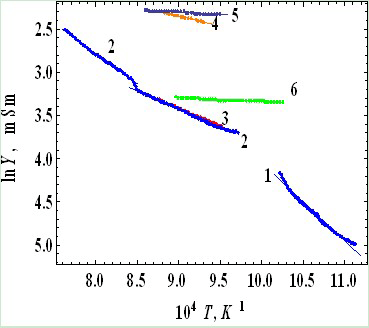 | Figure 7. Temperature dependence of the conductivity Y(T) after minimum for the samples of the doped glass1 (1) and glass2 (2 – 6) with RuO2 content about 16 wt % (1, 2), 20 wt% (3, 4) and 30 wt% (5, 6). Activation energy of conductivity Eσ is about (eV): 1.77 (1); 1.54 (2, lower T) and 0.93 (2, high T); 0.9 (3); 0.52 (4); 0.05 (5) and 0.047 (6). The solid lines are the fit of the experimental data to the expression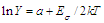 |
5. Conclusions
- 1. Narrow impurity subband close to the top of the glass valence band and spontaneously formed nanocrystals in the glass create conditions for simultaneous act of the activation and the hopping conductions at low temperatures. Cooperation of these mechanisms in DSG leads to the temperature dependence of resistivity in the form R(T) ~ exp(-K/Tζ) with 0.4 < ζ < 0.8 as it observed often in the experiments.2. It follows from the IR- and optical spectra that main factor of absorption in the RuO2 and DSG is the free carriers, whose concentration at room temperature is about 1020 cm-3 (gas of them is degenerate). Because of this the conductivity of the DSG varies negligibly at intermediate temperatures (77 K < T < 800 K).3. Increase of temperature up to 800 K leads to the structural transitions of nanocrystals in the DSG and interatomic distances race up. As a result the impurity subband splits off the top of the glass valence band and energy gap as wide as 0.095 – 1.52 eV opens up. Beyond the σ(T) minimum, concentration of free carriers decreases, degeneracy is lifted and the DSG turns into a typical semiconductor.
ACKNOWLEDGEMENTS
- Fund for Support of Fundamental Researches of the Uzbek Academy of Sciences is acknowledged for the financial support (grants 55-08 and 27-10).