-
Paper Information
- Paper Submission
-
Journal Information
- About This Journal
- Editorial Board
- Current Issue
- Archive
- Author Guidelines
- Contact Us
American Journal of Materials Science
p-ISSN: 2162-9382 e-ISSN: 2162-8424
2011; 1(1): 1-4
doi:10.5923/j.materials.20110101.01
Preparation and Characterization of Lithium Doped Silver Niobate Perovskite System
 Abstract
 Reference
 Full-Text PDF
 Full-text HTML
O. P. Nautiyal 1, S. C. Bhatt 2
1Uttarakhand Science Education and Research Centre (U-SERC), 33-Vasnt Vihar, Phase-II, Dehradun, 248006, India
2Department of Physics, H N B Garhwal University Srinagar, Uttarakhand 246174, India
Correspondence to: O. P. Nautiyal , Uttarakhand Science Education and Research Centre (U-SERC), 33-Vasnt Vihar, Phase-II, Dehradun, 248006, India.
| Email: |  |
Copyright © 2012 Scientific & Academic Publishing. All Rights Reserved.
Ceramic pellets of lithium doped silver niobate, Ag1-xLixNbO3 (x = 0, 0.3, 0.5 and 0.7), were prepared by solid-state reaction and sintering process. Niobium penta-oxide Nb2O5, silver oxide (Ag2O) and lithium carbonate (Li2CO3) were the starting materials. The prepared samples were characterized by XRD and SEM techniques. Grain sizes and lattice parameters were calculated by SEM and X-ray diffraction data for mixed Ag1-xLixNbO3 system. The variations in grain sizes and lattice parameters with composition at room temperature have been reported. All the samples show orthorhombic structure at room temperature.
Keywords: Silver Lithium Niobate, Perovskite Ceramics, Ferroelectrics, XRD, SEM
Cite this paper: O. P. Nautiyal , S. C. Bhatt , Preparation and Characterization of Lithium Doped Silver Niobate Perovskite System, American Journal of Materials Science, Vol. 1 No. 1, 2011, pp. 1-4. doi: 10.5923/j.materials.20110101.01.
Article Outline
1. Introduction
- The perovskite niobate (ANbO3) constitutes an interesting structural family, which undergoes several sequences and mechanisms of structural phase transitions. Silver lithium niobate (Ag1-xLixNbO3) system shows interesting properties[1, 2]. The constituents of this system are silver niobate (AgNbO3) and lithium niobate (LiNbO3). Silver niobate is known to exhibit several sequences and mechanisms of structural phase transitions as a function of the temperature[3-5]. Silver niobate AgNbO3 undergoes a sequence of phase transitions[6-8] observed at the following temperatures:(i) At 67℃, orthorhombic M1[FE] → orthorhombic M2[AFE]; (ii) At 267℃, orthorhombic M2[AFE] → orthorhombic M3[AFE]; (iii) At 353℃, orthorhombic M3[AFE] → orthorhombic O1[PE]; (iv) At 361℃, orthorhombic O1[PE] → orthorhombic O2[PE];(v) At 387℃, orthorhombic O2[PE] → tetragonal T[PE]; (vi) At 567℃, tetragonal T[PE] → cubic C[PE].where M1, M2 & M3 denote the phases with orthorhombic symmetry in rhombic orientation, while O1 & O2 are the phases with orthorhombic symmetry in parallel orientation. The parallel orientation means the orthorhombic axes are parallel to the pseudo cubic directions, whereas in the case of rhombic orientation the orthorhombic a- and b-axes are parallel to diagonals contained inside the faces of the same pseudo cubic axes[6]. It was established that M1 phase exhibit, weak ferroelectric[FE] properties, phase M2 & M3 are antiferroelectric[AFE] and phases O1, O2, T and C are paraelectric[PE][9]. The temperature evolution of the lattice parameters and the sequence of phase transitions are similar to those observed in sodium niobate (NaNbO3)[10, 11].Lithium niobate, LiNbO3 undergoes the phase transition at 1210 ˚C, from the trigonal[Ferroelectric] to the trigonal[Paraelectric]. Bhatt and Semwal[12] have reported dielectric properties of LiNbO3. The non- linear acoustical properties of LiNbO3 have led to the observation of a new physical effect. An acoustical tone burst stores energy with in the crystal that is re emitted at a later time of order of 70 μs. This effect can be characterized as an ‘acoustic memory’. This phenomenon is dependent on frequency and temperature[13]. X-ray investigations of Ag1-xLixNbO3 solid solution ceramics (0 ≤ x ≤ 0.15) showed that small Li substitution causes a change of symmetry[14]. At room temperature, a phase boundary between orthorhombic and rhombohedral symmetry is observed for x = 0.05; this phase boundary is indicated also by dielectric properties. The Li- substitution, leads to a gradual rise and shift of diffuse ε' (T) maximum which is observed for (AN) as 227℃. Instead of this diffuse maximum, a sharp one at 197 ℃ is already observed for Ag0.94Li0.06NbO3[14].
2. Material and Methods
- The final physical and electromechanical properties of ferroelectric material components greatly depend upon the preparation method used. For studies of fundamental properties of materials, large homogeneous single crystals are usually desirable to minimize the effects of surfaces and imperfections. However, single crystals are very expensive and difficult to grow, whereas ceramics have the advantage of being a great deal easier to prepare compare to their single crystal.
2.1. Sample Preparation
- The starting materials used for preparing silver lithium niobate Ag1-xLixNbO3 system were silver oxide (Ag2O), purity 97% (Qualigens Fine Chemicals); lithium carbonate (Li2CO3), purity 99% (Qualigens Fine Chemicals) and niobium pentaoxide (Nb2O5), purity 99.9% (Loba Chemie). Similar to preparation of silver niobate[7], silver sodium niobate[15,16], holmium doped lithium niobate[17] and silver potassium niobate[18,19], the samples of silver lithium niobate were prepared by solid-state reaction method. The starting materials were initially dried at 200ºC for 2h to remove the absorbed moisture and then quantities of the reagent required to prepare silver lithium niobate were weighed in stoichiometric proportion. All the samples were prepared according to following reaction:(1-x) Ag2O + x Li2CO3 + Nb2O5 → 2 Ag1-xLixNbO3 + x CO2Each composition was manually dry ground into fine powder for two and half hours and then wet mixed using reagent methyl alcohol and pestle for two hrs. The mixture was calcined in a silica crucible, in air, at 650 ºC for 2h, at 850 ºC for 2h and at 950 ºC for 1 ½ h.The pre-sintered mixture was ground again for 2h and pressed into pellets of 11 mm diameter applying the pressure of 3 tons. All pellets of a composition were placed on a silica crucible and sintered in air at 1000 ºC for 14h. All the samples were taken out from furnace when they cooled to room temperature. The sintered pellets of all compositions were gold polished for characterization (SEM) and electroded in metal-insulator-metal (MIM) configuration using air-drying silver paste for dielectric measurements. Prepared samples were characterized using XRD and SEM.
2.2. Characterization
- X-ray diffraction (XRD) patterns of all the prepared samples at room temperature have been obtained on a D-8 ANCE X-ray diffractometer (Bruker) using Cu-Kα radiation of 1.540598Å wavelength. The instrument was well calibrated with the silicon standard sample. Peak indexing was done by using JCPDS data. From the observed diffraction pattern, lattice spacing d was determined which was used to determine the lattice parameters. Surface topography of the samples was studied by scanning electron micrographs (SEM) using LEO-440 scanning electron microscope.
3. Results and Discussion
- The prepared ceramic samples of Ag1-xLixNbO3 for x = 0, 0.3, 0.5 and 0.7 were analyzed for phase and crystallinity by powder X-ray diffraction technique. X-ray diffraction pattern for all the samples were recorded at room temperature. The diffraction data were collected in the 2θ ranges of 10–70º with a scan step of 0.02º. X-ray diffraction patterns of obtained for all prepared samples is shown in Figure. 1. From the observed diffraction patterns the lattice spacing was determined which was used to determining the unitcell parameters. The unit-cell parameters were determined using the ‘WinPLOTR’ computer software (2005 version), which includes CRYSFIRE and FULLPROF software. From X-ray patterns, it was found that at room temperature all the compositions are in orthorhombic phase. Lattice parameters (Table 1) also reveal the structures of present systems.
 | Figure 1. Powder X-ray diffraction pattern of Ag1-xLixNbO3 for different x values. |
4. Conclusions
- In the present study, formation and characterization of lithium doped silver niobate perovskite system, Ag1-xLixNbO3 (x = 0, 0.3, 0.5, 0.7) have been investigated. Ceramic samples were prepared by solid state reaction and sintering method. The sintered samples were investigated for phase and crystallinity by powder X-ray diffraction. From X-ray diffraction patterns and SEM studies, it has been observed that at room temperature all the compositions are in orthorhombic phase. It was also found that average grain size of Ag1-xLixNbO3 decrease on increasing the value x, i.e., doping of Li. As Li is smaller than Ag, it causes a decrease in grain size on increasing concentration of lithium.
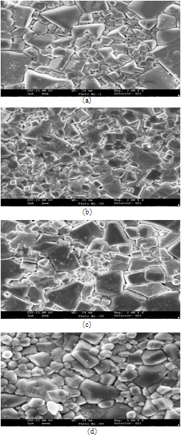 | Figure 2. Scanning Electron Micrographs of AgNbO3 (a), Ag0.7Li0.3NbO3 (b), Ag0.5Li0.5NbO3 (c) and Ag0.3Li0.7NbO3 (d) samples. |
ACKNOWLEDGEMENTS
- Authors express hearty thanks to Dr. Rajendra Dobhal, Director, USERC Dehradun, Uttarakhand, Dr. B.S. Semwal, Department of Physics, H.N.B. Garhwal University Srinagar, Uttarakhand, India and Dr. R.P. Pant, National Physical Laboratory, New Delhi, India for their help, support, constructive criticism & encouragement.
References
| [1] | Wada S., Saito A., Hoshina T., Kakemato H., Tsurumi T., Moriyoshi C., and Kuroiwa Y., 2007, Ferroelectrics 346, 64-71. |
| [2] | Kania A., and Miga S., 2001, Mater. Sci. Eng. B 86, 128-133. |
| [3] | Nautiyal O.P., Bhatt S.C., Pant R.P., and Semwal B.S., 2010, Indian J. Pure & Appl. Phys. 48, 357-362. |
| [4] | Kityk I.V., Makowska-Janusik M., Fontana M.D., Aillerie M. and Fahmi A., 2001, J. Applied Physics, 90, 5542. |
| [5] | Kania A., Roleder K., Kugel G.E., and Fontana M.D., 1986, J. Phys. C: Solid state Physics 19, 9. |
| [6] | Sciau Ph., Kania A., Dkhil B., Suard E., and Ratuszna A., 2004, J. Phys.: Condens. Matter 16, 2795. |
| [7] | Nautiyal O.P., Bhatt S.C., and Bartwal K.S., 2010, J. Alloys and Compouds, 505, 168-171. |
| [8] | Valant M., and Sarvorov D., 2006, J. Appl. Phys. 99, 124109. |
| [9] | Levin I., Krayzman V., Woicik J. C., Karapetrova J., Proffen T., Tucker M. G., and Reaney I. M., 2009, Phys. Rev., B 79, 104113 (14pp). |
| [10] | Bhatt S.C., Singh K., Uniyal M., Om Prakash, Singh P.K., Saxena R., and Semwal B.S., 2007, Indian J. Pure Appl. Phys. 45, 609. |
| [11] | Glazer A.M., and Megaw H., 1973, Acta Crystallogr.A 29, 489. |
| [12] | Bhatt S.C., and Semwal B.S., 1987, Indian J. Pure and Appl. Phys. 25, 174. |
| [13] | Michael S., Pherson Mc, Ostrovskit Igor, and Breazeale M.A., 2002, Phys. Rev. Lett. 89, 115506. |
| [14] | Nalbandinan V.B., Medviediev B.S., and Bieliayev I.N., 1980, Izv AN SSSR: Neorg. Mater. 16, 1819. |
| [15] | Nautiyal O.P., Bhatt S.C., Pant R.P., Bourai A.A., Singh P.K., Saxena R., and Semwal B.S., 2009, Indian J. Pure Appl. Phys. 47, 282. |
| [16] | S. C. Bhatt, O. P. Nautiyal, and B. S. Semwal, Processes and Characterisation of advanced nanostructured materials, Macmillan Publisher India Ltd, 2010, pp. 9-14. |
| [17] | Fadil F.Z., Aillerie M., Lamcharfi T., and Abdi F., 2011, Ceramics International, 37 (7), 2281. |
| [18] | Nautiyal O.P., Bhatt S.C., and Semwal B.S., 2009, Indian J. Pure Appl. Phys. 47, 719. |
| [19] | O. P. Nautiyal, S. C. Bhatt, and B. S. Semwal, Processes and Characterisation of advanced nanostructured materials, Macmillan Publisher India Ltd, 2010, pp. 3-8. |