-
Paper Information
- Next Paper
- Previous Paper
- Paper Submission
-
Journal Information
- About This Journal
- Editorial Board
- Current Issue
- Archive
- Author Guidelines
- Contact Us
Journal of Wireless Networking and Communications
p-ISSN: 2167-7328 e-ISSN: 2167-7336
2012; 2(5): 83-94
doi: 10.5923/j.jwnc.20120205.02
Envelope Tracking Line-up Design Considerations with High Efficiency Linearizable Inverse Class-F Driver Amplifier
 Abstract
 Reference
 Full-Text PDF
 Full-Text HTML
Zhancang Wang , Li Wang , Rui Ma , Xiao kun Yang , Sandro Lanfranco
Nokia Siemens Networks, Beijing/China, Mountain-View, USA
Correspondence to: Zhancang Wang , Nokia Siemens Networks, Beijing/China, Mountain-View, USA.
| Email: |  |
Copyright © 2012 Scientific & Academic Publishing. All Rights Reserved.
In this paper, comprehensive design considerations for multi-stage envelope tracking power amplifier line-up design with a 10W GaN HEMT switch mode driver amplifierwas presented to realized optimum overall power added efficiency.Crest factor reduction algorithm and non-linear switch mode driver design for efficiency and linearization were studied. Also, a high efficiency inverse class-F amplifier was implemented with efficiency as 44.8% for LTE 20MHz signaland characterized to provethe concept of applying linearizable inverse class-F amplifierenvelope tracking driver purpose.
Keywords: Crest factor Reduction, Efficiency,Envelope Tracking, GaN HEMT,Inverse Class-F,Line-up, Power Amplifier, Switch Mode
Cite this paper: Zhancang Wang , Li Wang , Rui Ma , Xiao kun Yang , Sandro Lanfranco , "Envelope Tracking Line-up Design Considerations with High Efficiency Linearizable Inverse Class-F Driver Amplifier", Journal of Wireless Networking and Communications, Vol. 2 No. 5, 2012, pp. 83-94. doi: 10.5923/j.jwnc.20120205.02.
Article Outline
1. Introduction
- In wireless communication infrastructure industry, to enhanceradio power amplifier (PA) efficiency, one of thepromising techniques is envelope tracking (ET). Principally, PA supply is varied based on the monitored envelope levelsand changing all the timeso as to right meet the output power level of PA at a certain moment of time to achieve high efficiency. With current high efficiency transistor technology such as GaN HEMT switch mode PA, final stage or single stage cannot achieve sufficiently high gain to keep the radio transistor line-up high efficiency. Lining up envelope tracking on both driver amplifiers and final stage is capable to boost overall or cascaded power added efficiency (PAE). Consequently, line-up envelope tracking can provide more improvement in radio efficiency, resulting in more profitable in a wireless system by cutting overall costs to operate the system, especially for high output power base stations.However, although it is highly desired to enhance the efficiency of driver amplifier by ET, choosing correct high efficiency PA topology with proper characterizations and considerations is critical to make a well matching between ET driver and final stage to maximize the performance of line-up. This paper mainly focuses on ET switch mode driveramplifier designconsiderations for system line-up, analysis and inverse class-F amplifier characterization for ET performance optimizations. Thenecessity of ET line-up for cascaded PAE was analysedmathematically in section II. In section III, the basic wide band supply modulator character was illustrated. A pieceof LTE 64QAM 20MHz signal source with featured clipping was used in this paper as stimulus for analysis. The relationship between ET and clipped signal probability density function (PDF), instantaneous peak error vector magnitude (EVM) were discussed in section IV. In section V, with regard of inverse class-F topology, a 10W switch mode driver amplifier was designed and characterized based on GaN HEMT technology. Linearization capability of this kind of high efficiency driver was studied as well. Finally, conclusions were given in section VI.
2. Power-Added Efficiency& ET PA Line-Up
- Power-added efficiency (PAE) is an important metric for ET PA efficiency in that it is not only a measure of efficiency, but also taking all of the power input into consideration, which means for the ET PAs producing the same output power, the ones with higher PAE will ultimately work for a longer time if the same amount of energy was provided.However, in ET PA working scenarios, it operates in the compression region over most of envelopes, usually being pushed seriously into saturation in short instants, resultingin gain loss for final stage, which finally reduces the PAE of ET PA to some extent. According to the below analysis in Fig.2 and gain character of commercial GaN HEMT transistors, the gain threshold is set at about 10dB for ET PAs,below which overall efficiency, orPAE, will start to degradeseriously. Therefore, ET PA line-up is taken into account bysharing one modulator to further increase PAE of an ET PA design, as shown in Fig.1.The drain or collector efficiency of PA is defined as
 | (1) |
 | (2) |
 | (3) |
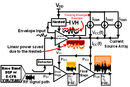 | Figure 1. ET PA line-up block diagram including modulator schematic |
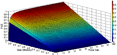 | Figure 2. PAE character plot vs. power gain and drain efficiency |
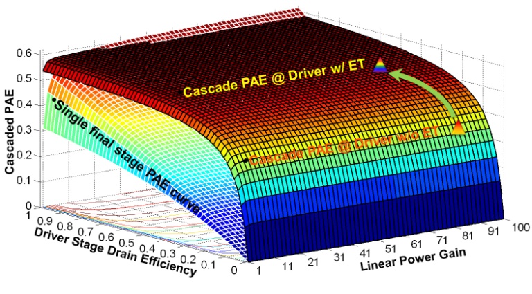 | Figure 3. Line-up cascaded PAE character vs. driver amplifier power gain and its drain efficiency compared to a single stage PA |
3. Wideband Supply Modulator
- The architecture of supply modulator in this paper was illustrated in [2]. The modulator bandwidth requirement is challenging due to the character of envelope spectrum. Although the envelope signal power of LTE takes the loin share of power, about 96%, within its RF signal bandwidth from DC, e.g. 100MHz LTE-Advanced envelope spectrum shown in Fig.4, the modulator bandwidth should be designed with five times of RF bandwidth, considering both amplitude and phase spectrum shape of envelope.However, switching supply fails to provide high efficiency for such a high speed, the switching loss is tremendous. Therefore, linear modulator part needs to boost efficiency for wider bandwidth applications, which can be implemented by the proposed nested structure by adding an additional peak efficiency point into linear part modulator [2], as shown in Fig.5.In Fig.5, the green and blue simulation results are the instantaneous efficiency of linear part with nested voltage ratio α =2/3 & 1/2 respectively, trying to fit envelope voltage PDF of LTE 20MHz 64QAM signal with the other peak efficiency point, boosting the efficiency of the wide band linear modulator.
 | Figure 4. In LTE-Advanced with 100MHz signal bandwidth, in-band 100MHz bandwidth takes up 96% power of the envelope signal |
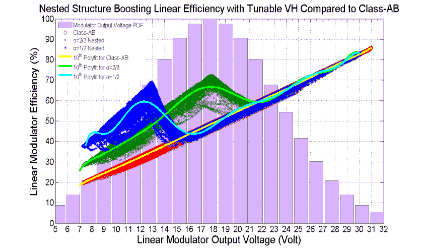 | Figure 5. Nestedstructureefficiency boosting simulation results with a LTE 20MHz 64QAM compared to Class-AB linear part |
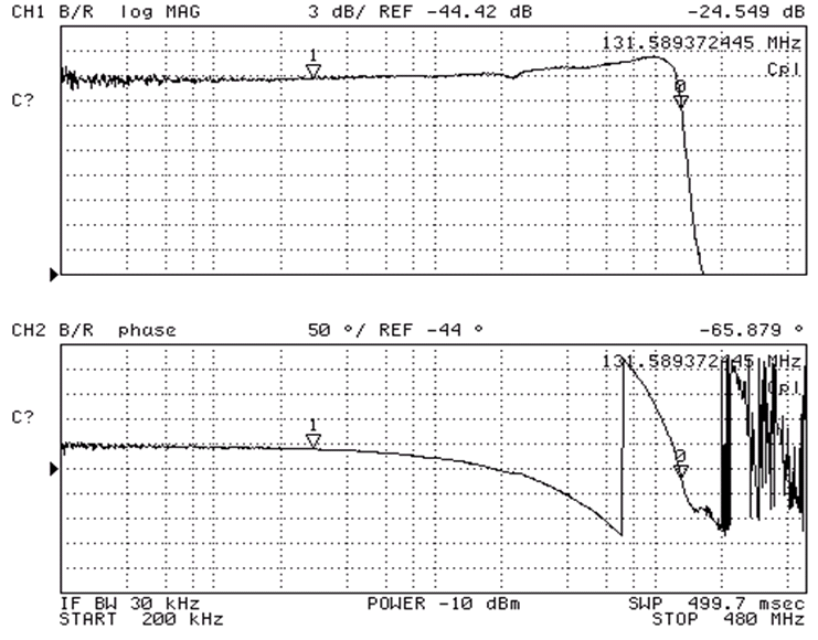 | Figure 6. Frequency response measurement results of the modulatorwith a resistive load |
 | Figure 7. Various clippings of CFR shift the PDF of LTE 20MHz right forward to fit the final ET amplifier stage trajectory |
4. Crest Factor Reduction Algorithm for ET
- Traditionally, the crest factor reduction (CFR) algorithm contains the crest of modulated signal into PA to make operation possible in higher efficiency region. However, the benefit of CFR algorithm to ET PA efficiency is also obvious.
4.1. CFR Analysis for ET PA
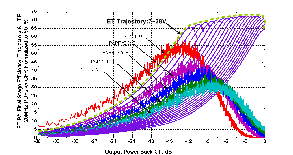
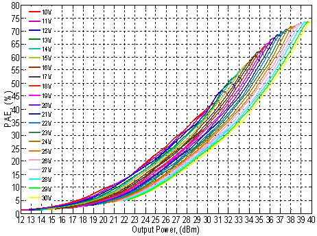
- Since the modulation schemes at base band are getting ever more complex, the peak to average power ratio (PAPR) is ever larger and moving toward left side in probability density function (PDF) plot. However, CFR is capable to move it toward right side, avoiding RF PA suffering from too much back-off resulting in average efficiency degradations. Also, in ET scenarios, CFR can make PDF histogram shape more fit for efficiency trajectory of a RF PA transistor with various drain or collector voltages as shown in Fig.7.In Fig.7, ET trajectory was tested and plotted in dashed green by short RF pulse measurement method for the ET PA final stage with supply voltage ranging from7V to 28V. The maximum CW output power was normalized into 0dBm to easily compare it with different LTE 64QAM 20MHz PAPRs with clipping ranging from 5.5dB to no clipping scenario. About 6dB movement in maximum to the right of the peak probability of PDF was observed. Besides, the probability of occurrence in smaller back-off region has increased significantly. Thereafter, well-clipped modulated signal will fit better into the shape of ET PA trajectory to obtain more efficiency.In ET PA system, the linear plot of LTE PDF versus supply modulator output voltage could make the effects of clipping to drain or collector modulation more clearly in Fig.8.
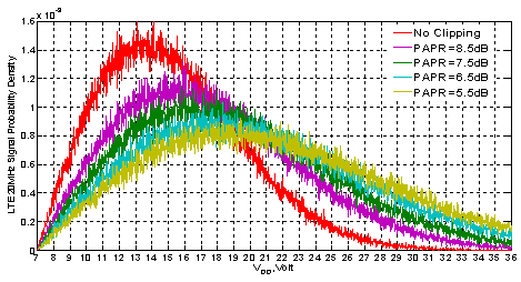 | Figure 8. The PDF of LTE 20MHz versus ET modulator output voltage |
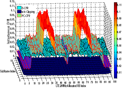 | Figure 9. 3D plot of instantaneous EVM vs. allocated RBs and sub-frames in LTE 20MHz to compare performance between PC-CFR and proposed E-CFR |
4.2. The Proposed Equalized CFR for ET PA
- There is a trade-off among more crest reduction, spectrum re-growth and error vector magnitude (EVM) degradations. Therefore, CFR algorithms have been studied for the most optimized performance. Peak-Cancellation CFR (PC-CFR) is one of most popular solutions in practical applications. However, it may suffer from serious peak EVM degradations, resulting in lower throughput of base station when clipping is required too hard.The proposed equalized CFR (E-CFR) algorithm is capable to optimize or equalize instantaneous or peak EVM crossing LTE allocated resource blocks (RBs) and sub-frames, which causes a flat response of EVM overall various with the two axis shown as the 3D plot in Fig.9.Accordingly, both composite and instantaneous peak EVMs with E-CFR are lower than PC-CFR, resulting in a much better EVM when clipping is hard as shown in Fig.9 and Table I, e.g. clipped PAPR=6.5dB, EVM under PC-CFR was 5.32%; EVM under E-CFR was 3.21% which is ~ 2% improvement. In the other word, with E-CFR for ET purpose, more clipping can be implemented for better efficiency performance without much degrading modulation quality.
|
5. Experimental Inverse Class-F Amplifier for ET
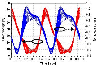
- To obtain higher efficiency of RF PA for the line-up driver design, one effective way is to utilize harmonic manipulation to realize a switching mode inverse Class-F amplifier. By means of this art, the amplifier has to operate in saturation region and resulting in serious distortions. However, with modern digital pre-distortion (DPD) technology, it could be linearized accepted level to satisfy the specifications by careful and sophisticated design. In this work, an inverse Class-F based on CREE 10W GaN HMET transistor CGH40010 was designed for envelope tracking line-up driver purpose as shown in Fig. 10, which required “friendly” character or optimized memory effect to pre-distortion.With the principle of an inverse Class-F RF amplifier, the high efficiency operation was obtained by manipulating limited even and odd harmonics, e.g. only 2nd and 3rd order harmonics of fundamental frequency were considered to generate a quasi-half-sinusoidal voltage waveform and a quasi-square current waveform at the transistor output. In practical design, compensation transmission lines for the parasitic of bonding wire inductance in series and package plane were considered. The micro stripcompensation and matching network design was verified by simulations in package plane. The required loading condition was implemented by control of the device non-linear output capacitance and parasitic inductance. The simulated inverse class-F instantaneous voltage and current waveforms with the harmonic terminations were as shown in Fig. 11 below. The phase difference between voltage and current was approaching to zero, realizing high efficiency on the resistive fundamental load impedance.
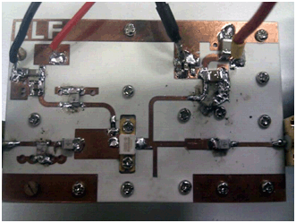 | Figure 10. Realized inverse class-F 10W driver amplifier |
 | Figure 11. Simulated inverse class-F instantaneous waveforms at package plane of a 10W GaN HEMT transistor |
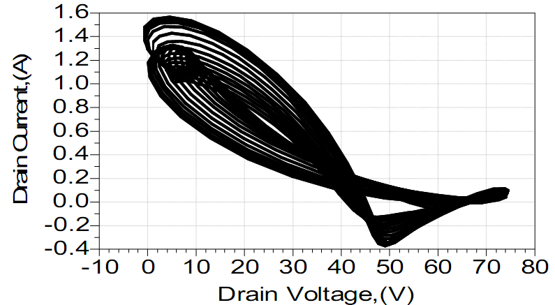 | Figure 12. Simulated inverse class-F load lines at package plane of a 10W GaN HEMT transistor |
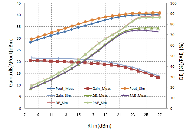 | Figure 13. Measured power sweep test results compared to simulation data of the inverse class-F design at 2.14GHz |
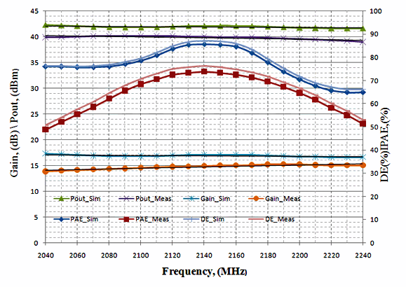 | Figure 14. Measured frequency sweep test with 25dBm input level results compared to simulation data of the inverse class-F design at 2.14GHz |
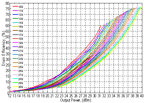 | Figure 15. Measured inverse class-F driver ET drain efficiency trajectory with RF CW pulse amplitude sweep |
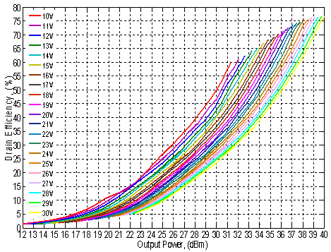 | Figure 16. Measured inverse class-F driver ET gain efficiency trajectory with RF CW pulse amplitude sweep |
 | Figure 17. Measured inverse class-F driver ET PAE efficiency trajectory with RF CW pulse amplitude sweep |
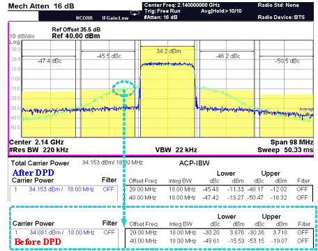 | Figure 18. Measured PA output spectrum before and after DPD with 20MHz LTE signal, on 30V fixed supply |
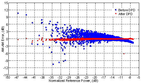 | Figure 19. Measured AM-AM response before and after DPD with 20MHz LTE signal |
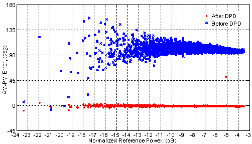 | Figure 20. Measured AM-PM response before and after DPD with 20MHz LTE signal |
6. Conclusions
- In this paper, comprehensive design considerations for multi-stage envelope tracking power amplifier line-up was analysed and concluded. The benefit of lining up ET amplifiers over other topologies are obvious and it could make more profit in a radio system by cutting overall costs due to higher efficiency with higher PAE. The line-up PAE character was analysed that it produced a constant PAE response varied with driver amplifier collector or drain efficiency, superior to single final stage solution. In section III, the wideband ET modulator with nested structure was introduced to further boost modulator efficiency. E-CFR was proposed to reduce both the peak and composite EVM of LTE signal during clipping, which could make the PDF more fit for the ET efficiency trajectory. Also, a 10W inverse class-F driver amplifier based on GaN HEMT was implemented with good linearization capability. With 30V fixed supply, when DPD was implemented and became stable, while kept the output power level the same, ACLR was -45.5dBc, kept approaching the threshold of 3GPP requirement of -45dBc, the efficiency was 44.8% with a power gain of 17.9dB. When the amplifier was implemented with ET, kept the linearity specifications, drain efficiency was boosted from 39.9% to 64%, excluding efficiency of ET modulator.