I. Akhchaf 1, S. Khoulji 2, M. Essaidi 3, M. L. Kerkeb 3
1Information and Telecommunications Systems Laboratory, Faculty of Sciences Abdelmalek Essaadi University Tetuan, Morocco
2Department of Statistics and Informatics, Faculty polydisciplinary of Tetouan, Tetuan, Morocco
3Physics Department, Faculty of Sciences of Tetouan, Morocco
Correspondence to: S. Khoulji , Department of Statistics and Informatics, Faculty polydisciplinary of Tetouan, Tetuan, Morocco.
| Email: |  |
Copyright © 2012 Scientific & Academic Publishing. All Rights Reserved.
Abstract
The new current design is especially suitable for use in multi-standard wireless receiver for microwaves communication systems. In recent years, there1.34 dB with 12.06 dB. has been a growing market for dual band transceivers for various wireless standards. This work investigates a novel circuit topology of concurrent Dual-band Low Noise Amplifier (LNA) operates in the 3.9 GHz and 4.48 GHz frequency bands for WLAN applications and may be used for dual band cellular applications. RF circuit designs take two parallel LNAs with a single transistor only, and band-pass filter (BPF) networks are usually used match both the input and output ports at two different bands, are matched to 50Ω without external elements. The transistor ATF1 0136 is chosen for the purpose of high gain and low noise characteristics. Simulations of the operation of the amplifier were performed with the software ADS and Ansoft software and performance of the amplifier were recorded and analyzed. Simulation results indicate a Noise Figure NF below 1.5dB and a gain S21 above 11 dB in all frequency bands and also input and output return loss are below -11 dB for all desired frequency band while drawing 2.5mA current from a 5V power supply. The chip provides a good basis for the realization of WLAN low-cost RF receivers for dual-band operation. These performances situate this receiver among the most competitive low cost and low power RF receivers. All the principles carry out in this work are furthermore transposable to other frequencies and to other transmission standards.
Keywords:
Microwaves Communication Systems, Wireless Receiver, System Radio Frequency (RF), Band-Pass Filter (BPF) , Low Noise Amplifiers (LNA), Dual Band Amplifiers, Advanced Design System (ADS)
Cite this paper:
I. Akhchaf , S. Khoulji , M. Essaidi , M. L. Kerkeb , "Study, Modeling and Characterization of Dual-Band LNA Amplifiers Receivers for Wireless Microwaves Communication Systems", Journal of Wireless Networking and Communications, Vol. 2 No. 5, 2012, pp. 77-82. doi: 10.5923/j.jwnc.20120205.01.
1. Introduction
In recent years, there has been a growing market for dual band transceivers for various wireless standards. WLANs (wireless local-area networks) have been deployed all over the world as office and home communication infrastructures. The increasing demand has motivated the introduction of new WLAN standards such as IEEE 802.11a and IEEE 802.11g to meet various application requirements. However, the diversification of the WLAN standards poses significant challenges in the design of the RF front-ends. It is desirable to have a system that can support multi-standard operations while maintaining a competitive hardware cost. Using conventional receiver architectures, simultaneous operation at different frequency bands can only be achieved by building multiple independent signal paths with an inevitable increase in the cost, footprint, and power dissipation[1-2]. Figure 1 illustrates the receiving band distribution of current wireless communication standards in the range of 2.3GHz-6GHz. 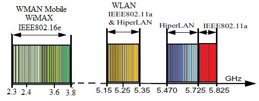 | Figure 1. Receiving band distribution of current wireless communication stands in the range of 2.3-GHz-6GHz |
With so many communication standards, one may consider to develop multi-functional devices, which can operate at several bands and different modes. However, traditional multifunction device is often bulky and power hungry in general, which limits the size, weight and the battery life of the wireless communication devices[3-5]. Thus, development of a single-chip multi-function RF receiver with low-cost, low-power and small form-factor characteristics is in demand[4-5].In this work, new concurrent dual-band receiver architecture is introduced that is capable of simultaneous operation at two different frequencies. These new concurrent dual band LNAs provide simultaneous narrow-band input matching and gain at dual frequency bands, while maintaining low noise.Modern communication applications require easy translation across different communication protocols. This is one of the primary reasons why design of multi-standard receivers is of such importance in any RF system. Low Noise Amplifiers (LNAs) represent one of the key front-end blocks of RF wireless systems. THE low-noise amplifier (LNA) for radio systems is one of the most critical components in the radio front-end. A receiver requires better receiver sensitivity and a lower noise figure, for example, an IEEE 802.11a receiver. The expected receiver sensitivity can be achieved by an optimal design of the LNA in terms of a near-to-minimum noise figure and reasonable power gain over the entire band. On one hand, classical wideband amplifier topologies, e.g., feedback and distributed amplifiers, small area, and low cost. On the other hand, an LNA implemented with multiband matching networks provides more degrees-of-freedom to achieve both a low noise figure and flat power gain without increasing the power consumption. However, as the dual band input and output matching networks have more circuit components, the LNA noise figure and power gain can be more sensitive to the statistical variations of the passive components[3-4],[7].The linearity of a Si bipolar junction transistor (BJT) or a SiGe HBT can be reliably improved using a simple technique based on low-frequency low-impedance base termination without degrading gain or NF. However, this technique is not effective for linearizing field-effect transistor (FET) amplifiers. An FET can also be linearized by biasing at a gate–source voltage (Vgs) at which the third-order derivative of its dc transfer characteristic is zero. The bipolar junction transistor was the first solid-state active device to provide practical gain and NF at microwave frequencies. In the seventies, breakthroughs in the development of field-effect transistors (FETs) (e.g., GaAs MESFET) led to higher gain and lower NF than bipolar transistors for the frequencies in the range of several GHz. Currently, advanced FETs and bipolar transistors still compete for lower NF and higher gain at frequencies in excess of 100 GHz. Examples are the high electron-mobility transistors (HEMTs), such as pseudomorphic high electron-mobility transistors (pHEMTs), metamorphic high electron-mobility transistors (MHEMTs), as well as heterojunction bipolar transistors (HBTs), built using a variety of semiconductor materials (e.g., GaAs, InP, Si, SiGe)[1].The design considerations of low-noise amplifier are mainly in input return loss, power gain, and noise figure (NF), but there are some trade-off between these important characteristics. At the input, network consisting of two filters PBF is used two different frequency bands at 3.9 GHz and 4.48 GHz. The impedance of the input matching network is 50Ω, and the same thing to the output. In this paper, the complete circuit is simulated by Agilent Advanced Design System (ADS), Section 2 describes the design of the proposed dual-band LNA. Simulations results are shown in Section 3 and conclusions are given in Section 4.
2. Circuit Design
In this paper dual band LNA designs with lumped and distributed-matching networks are studied. The simplified schematics of the LNA implementations are shown in Figure 2. First, sensitivity analyses of the noise figure matching condition in response to frequency are done with regard to passive component tolerances. Then, simulations including real-world lumped passive component tolerances, and for the distributed matching networks, manufacturing process tolerances are performed in advanced design system (ADS) from Agilent Technologies [2].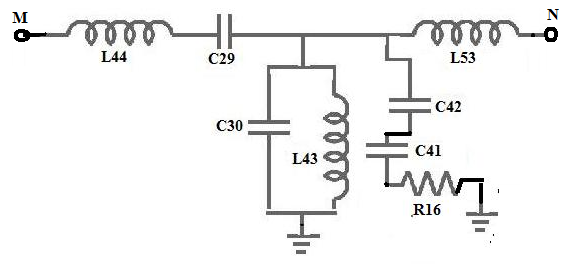 | Figure 2. The simplified schematics of the LNA implementations |
In this section, we will develop a concurrent dual-band receiver architecture that can be fully integrated. The objective is to devise a receiver that can simultaneously receive the signal at two different frequency bands with maximum reuse of power. While the input and output of a stand-alone LNA usually needs to be matched to 50Ω. LNA with dual band distributed matching networks is designed circuit board process aiming for a low noise figure and a flat power gain over the entire 3.7–4.5 GHz bandwidth. As shown in Figure.3, the input matching network of two filters BPF the input and adaptation of transistor ATF10136, which will be tuned to 3.9 GHz and 4.48 GHz. the input impedance to 50Ω. The transistor ATF10136 is chosen for the purpose of high gain and low noise characteristics.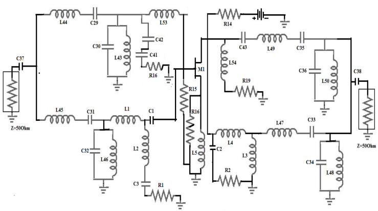 | Figure 3. Schematic of the proposed dual-band LNA with only one transistor |
The transistor ATF-10136 is a high performance gallium arsenide Schottky-barriergate field effect transistor housed in a cost effective microstrip package. Its premium noise figure makes this device appropriate for use in the first stage of low noise amplifiers operating in the 0.5-12 GHz frequency range. This GaAs FET device has a nominal 0.3 micron gate length using airbridge interconnects between drain fingers. Total gate periphery is 500 microns. Proven gold based metallization systems and nitride passivation assure a rugged, reliable device.The first component of wireless communication receiver is typically a low noise amplifier (LNA). It main role is to provide enough gain to overcome the noise of subsequent stages. An LNA not only providing this gain while adding as little noise as possible, but also should accommodate large signals without distortion, and frequently must also present a specific impedance, such as 50 Ω , to the input source. In order to get better linearity and noise performance, we should make the noise figure and distortion as small as possible in LNA part to meet the receiver sensitivity. Assume that the two operating angular frequencies of the target BPF and LNA are ω1 and ω2 (ω1<ω2), respectively. There are two filter BPFs connected with the MN as shown in figure 2. Second, in the Smith Chart, for each operating frequency, find the appropriate source and load reflection coefficients, which can satisfy the desired gain and noise figure. Then, design the single-band input A and output B for two single-band LNAs[5].Figure 3 is concurrent dual-band LNA architecture based in the one transistor ATF technology. In the input, there are parallel two filters BPF, the proposed low-noise amplifier consists the input matching network which is implemented by the Filter BPF where are L1, C1, L2, C2 and Ls; the main amplifier is containing M1, the Cdc1, Cdc2 are DC blocking capacitors. In input matching, for simultaneous power and noise matching at dual frequencies, the real part of Zin has matched to 50Ω and the imaginary part of Zin will be zero. The first active element in the receiver chain, the noise figure (NF) of an LNA plays a significant role in the overall NF of the receiver, which controls its sensitivity and output signal-to-noise ratio (SNR). Inductive source degeneration is used for input matching. This also increases the stability of the LNA through negative feedback at the expense of lower gain[1],[8-[9]. The bias circuit is very critical for the overall noise performance of the LNA. The bias current in the LNA does not need to be exact because feedback in the LNA’s input stage stabilizes its performance over production. Considering the design goal, the transistor ATF with bias condition of Ic = 2.5 mA and VCE= 5 V is used in the design. In order to improve the stability, an inductor of 0.09 nH is connected with the emitter of the transistor.In RF wireless receiver, LNA is one of the most critical building blocks caused by the noise figure is dominated in 1st stage of the receiver. For LNA design, there are many trade-off between different performances. For example, the power gain affects noise figure, the die area affect cost, and the power consumption affects the battery life.The circuit is designed on the substrate FR4 with a relative dielectric constant of 4.4 and a thickness of 1.5 mm and two software’s Ansoft Designer and ADS is used to simulate the circuit. As shown in Fig.2, the simulated fractional bandwidth, Gain and NF after design are 11.95 dB and 1.39 dB at 3.9 GHz, 12.06 dB and 1.34 dB at 4.48 GHz, respectively[5].For measurement consideration, the output impedance is always designed in 50 Ω in the output buffer. The design considerations of low-noise amplifier are mainly in input return loss, power gain, and noise figure (NF). The resulting Miller impedance therefore acts like a noiseless shunt resistor at the input. By appropriate choose of and it is thus possible to artificially move the LNA’s input impedance towards the 50 Ω points in the Smith Chart without affecting its optimum noise impedance or increasing its minimum noise figure.It is crucial to note the fundamental differences between the concurrent and the existing no concurrent approaches. In conventional dual-band LNAs, either one of the two single-band LNAs is selected according to the instantaneous band of operation, or two single-band LNAs are designed to work in parallel using two separate input matching circuits and one separate resonant loads.We use a general model for an amplifier in the source impedance (Zs) configuration to obtain an equivalent circuit for the input impedance and a general expression for the gain at dual frequencies. This equivalent circuit will be used to achieve simultaneous power and noise matching in a concurrent dual band LNA.Theoretically, a large number of passive topologies for and can provide input impedance matching and output impedance matching at dual frequency bands. In this circuit was made input adaptation and output by Smith Chart. The Smith Chart, for each operating frequency, find the appropriate source and load reflection coefficients, which can satisfy the desired gain and noise figure[1-5].The transistor is not a perfectly unilateral component. These are the multiple internal feedbacks that create a dependency of the input towards of the output in the real component. It is possible to correct for these effects while working on external feedback that will compensate for these phenomena.When a circuit is unstable, it is often that it has too much gain. This condition associated with a phase condition which in this case did not need to be perfect, is the start of oscillation or a more complex phenomenon still.To control this setting, it is always possible to add dissipative elements (resistors), the ideal of course is that these resistors dissipate power main frequencies where we expect problems, and disrupt the low point’s useful frequencies. We therefore propose to add to the amplifier two resistors of stabilization (input-output), as shown in figure 3.If the noise factor is too large, this is stabilizing resistance placed in input (the thermal noise is amplified by the transistor which degrades the high NF). We can then use resonant circuits in the sensitive circuit of frequency stabilizing resistances.An important design parameter in receiver design, which is the measure of receiver noise, is the noise factor F (also known as NF, when expressed in decibels). The definition of the noise factor of any transducer (e.g., LNA, mixer, filter, etc.) given by[6] is: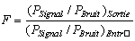 The value of the noise figure NF characterized by:
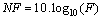 The stability k of an LNA amplifier circuit can also be studied with the help of the Rolett factor as given in Table 1. This is more useful when viewing larger frequency spectral.
 Where:
  To design an unconditionally stable LNA amplifier circuit, which implies that the amplifier remains stable within the entire domain of the Smith Chart at the selected frequency and the given bias conditions, the following conditions must be met. As well as
| Table 1. Stability of the proposed dual band LNA for 3.9 GHz and 4.48 GHz frequency bands |
| | Frequency | 3.9GHz | 4.48GHz | | K | 1.05 | 1.01 | | ∆ | 0.404 | 0.230 |
|
|
If an RF amplifier is determined to be unstable, and its function calls for stability, a stabilising network is needed. One way to stabilise an RF LNA amplifier is to add a series or shunt resistor to either input or output port, preferably to the output port since a resistor produces noise which is undesirable to amplify.
3. Results and Discussion
A novel circuit topology for dual-band LNA with a single-input FET, the input matching conditions are satisfied by switching the finger number and the bias voltage of the input transistor. A 3.7/4.48-GHz dual-band LNA was designed and implemented. The input parallel resonator and series is made using filter BPF1 a 0.44-pF capacitor and a 7.15-nH inductor parallel and a 0.37-pF capacitor and a 0.13-nH inductor series.This section presents the simulation results of a concurrent dual-band LNA operating at 3.9GHz and 4.48GHz frequency bands for wireless communications. The design is based on the topology of Figure 3; The proposed dual-band LNA (Figure 3) is simulated with the software ADS and Ansoft software. Figure 4 to Figure 6 illustrate the simulation results of S-parameters and NF data respectively, as a function of frequency. At 3.9GHz, a NF of 1.39 dB is achieved with 11.95 dB gain. At 4.48GHz, the NF is 1.34 dB with 12.06 dB. Figure 4(a) shows the noise figure maximum (NF) and Figure 4(b) shows the noise figure minimum (NFmin) of this LNA. At 3.9 GHz, the maximum noise figure is 2.00 dB and the minimum is 1.44 dB. At 4.48 GHz, the maximum noise figure is 3.23 dB and the minimum 1.34 dB. The noise figure is higher than that of a single-stage LNA because the input matching network contains two inductors, in which the parasitic resistance will increase the noise figure. The LNA’s noise performance is quite satisfactory. Table 2 summarizes the performance of the current design. | Figure 4. Noise Figure NF(a) and NFmin (b) of the proposed dual band LNA |
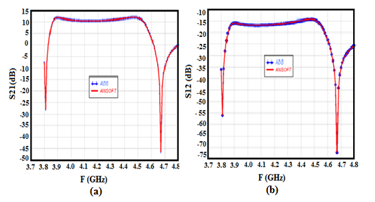 | Figure 5. Gain (a) and reverse isolation (b) of the proposed dual band LNA |
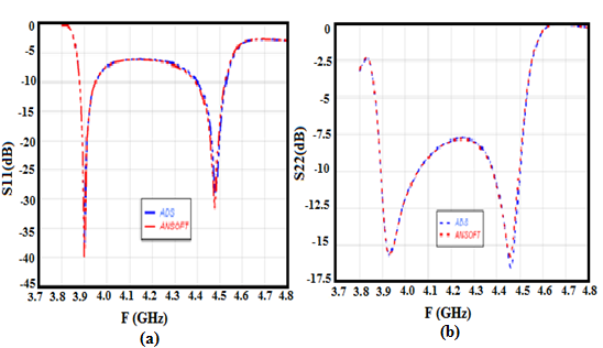 | Figure 6. Input (a) and output (b) reflection coefficient of the of the proposed dual band LNA |
| Table 2. Performance Summary of the Concurrent Dual Band LNA |
| | Frequency | 3.9 GHz | 4.48GHz | | Voltage Gain | 11.95dB | 12.06 dB | | S11 | -20.00dB | -15.00 dB | | S22 | -12.50 dB | -12.50 dB | | S12 | -16.00dB | -15.00dB | | NF/NF min | 2.00 dB/1.39dB | 3.23dB/1.34dB | | Power consumption | 13.8 mW | | DC Current | 2.5mA | | Supply Voltage | 5V |
|
|
The amplifier works at 5 V supply voltage with 2.5 mA current dissipation. Figure 5 shows the gain (S21) of this LNA in different bands. The maximum gain is 11.95 dB at 3.9 GHz, and is 12.06 dB at 4.48 GHz. The dynamic range of gain is 11 dB and an interval of about 1 dB at both 3.9 GHz and 4.48 GHz. Figure 6 shows the input return loss and output return loss, respectively, of this LNA. Both are lower than −10 dB in two bands frequency bands showing that the LNA exhibits good input matching at two frequencies. The maximum power consumption is 13.8 mW, under a power supply voltage of 5 V. And we have demonstrated its good performance through other software Ansoft post simulation results.
4. Conclusions
The new concept of concurrent dual band LNA amplifiers receivers for wireless microwaves communication systems, with the intention of use as the essential part of a concurrent dual band receiver is designed. One implementation of such new concurrent dual-band receiver architecture capable of simultaneous operation at two different frequency bands is analysed. It uses a novel concurrent dual-band LNA, combined with an elaborate frequency conversion scheme to reject the out-of-band signals. A general methodology is also provided to achieve simultaneous narrow-band gain and input matching while offering a low NF in concurrent dual band LNAs. The proposed dual-band LNA can be used for the Bluetooth, HiperLAN and Wireless LAN (IEEE 802.11a) communication applications, and is designed based on transistor ATF10136 technology, which has better performance, lower cost and better integration feasibility comparing with other technology. The RF input signals are 3.9GHz and 4.48GHz, respectively. It is operating at supply voltage of 5V. The circuit is simulated using Agilent Advanced design system (ADS) and Ansoft software. By filtering characteristics of input stage, the LNA can selectively receive signals in multi-band.
References
| [1] | S. Wang and B.-Z. Huang, "A HIGH-GAIN CMOS LNA FOR 2.4/5.2-GHZ WLANAPPLICATIONS", Progress In Electromagnetics Research C, Vol. 21, Page(s): 155-167, 2011. |
| [2] | Erick Emmanuel Djoumessi and Ke Wu, "Dual-Band Low-Noise Amplifier Using Step-Impedance Resonator (SIR) Technique for Wireless System Applications",Proceedings of the 39th European Microwave Conference; , Rome, Italy, 978-2-87487-011-8 EuMA 29 September, Page(s): 1307-1310 October 2009. |
| [3] | Sambit Datta, Kunal Datta, Ashudeb Dutta, and Tarun Kanti Bhattacharyya, "Fully Concurrent Dual-Band LNA Operating in 900 MHz/2.4 GHz Bands for Multi-Standard Wireless Receiver with sub-2dB Noise Figure", ICETET, 3rd International Conference on Emerging Trends in Engineering and Technology, Page(s): 731-734, 2010. |
| [4] | Adriana Serban, Magnus Karlsson, and Shaofang Gong, "Component Tolerance Effect on Ultra-Wideband Low Noise Amplifier Performance", IEEE Transactions on Advanced Packaging, Vol. 33 , No. 3 , Page(s): 660 - 668, Aug. 2011 |
| [5] | Runbo Ma and Wenmei Zhang, "Co design of Dual-band Low Noise Amplifier and Band-pass Filter", Asia-Pacific Symposium on Electromagnetic Compatibility (APEMC), IEEE, 2010, Page(s): 1378 – 1380, june 2010. |
| [6] | Kai Xuan,1 Kim Fung Tsang,1 and Wah Ching Lee2, “a novel tunable dual-band low noise amplifier for 868/915 mhz and 2.4 ghz zigbee application by cmos technology", Wiley Periodicals, Inc. Microwave and Optical Technology Letters , Vol. 52, No. 3, pages 507–510, March 2010. |
| [7] | Sambit Datta, Kunal Datta, Ashudeb Dutta, and Tarun Kanti Bhattacharyya, "A Concurrent Low-Area Dual Band 0.9/2.4 GHz LNA in 0.13μm RF CMOS Technology for Multi-Band Wireless Receiver", IEEE Asia Pacific Conference on Circuits and Systems (APCCAS), Page(s): 280 – 283, May 2010. |
| [8] | Kyoohyun Lim ,"A 2x2 MIMO Tri-Band Dual-Mode Direct-Conversion CMOS Transceiver for Worldwide WiMAX/WLAN Applications", IEEE Journal of Solid-State Circuits, Vol. 46 , No. 7 , Page(s): 1648 – 1658, July 2011. |
| [9] | Zhe-Yang Huang1, and Chung-Chih Hung, “CMOS Dual-Band Low-Noise Amplifier for World-Wide WiMedia Ultra Wideband Wireless Personal Area Network System", Microwave Conference Proceedings (APMC), 2010 Asia-Pacific, Page(s): 334 – 337, March 2011. |
 Abstract
 Reference
 Full-Text PDF
 Full-Text HTML