S. Syed Ameer Abbas1, A. Kanimozhi1, S. J. Thiruvengadam2
1Department of Electronics and Communication Engineering, Mepco Schlenk Engineering College, Sivakasi, 626005, India
2Department of Electronics and Communication Engineering, Thiagarajar College of Engineering, Madura, 625015, India
Correspondence to: S. Syed Ameer Abbas, Department of Electronics and Communication Engineering, Mepco Schlenk Engineering College, Sivakasi, 626005, India.
| Email: |  |
Copyright © 2012 Scientific & Academic Publishing. All Rights Reserved.
Abstract
Wireless network has been improved after 3G by means of higher data rates with better coverage and by reducing latency. LTE is the technology that provides backward compatibility with 3G and 4G technologies. Compared with 3G, it offers high data rates of the order of 50Mbps for uplink and 100Mbps for downlink. LTE is able to provide services in scalable bandwidth (1.4, 3, 5, 10, 15 or 20 MHz). It uses the frame structure as Time Division Duplexing (TDD) and Frequency Division Duplexing (FDD). LTE technology uses different channels in both links for different applications. This paper mainly focuses on downlink channels, particularly data channels named as PDSCH, PBCH and PMCH. The main objective of this paper is the realization of the SISO (Single Input- Single Output) architecture of PBCH downlink data channel with its own transmitter and receiver. Information is processed at transmitter by means of scrambling, modulation, layer mapping, precoding and mapping to resource elements. Similar to the transmitter, receiver also has to perform some techniques to retrieve the original data such as demapping from resource elements, decoding, delayer mapping, demodulation and descrambling. Simulation of these steps for transmitter is done by using ModelSim 6.4a and the synthesis and implementation are done by using PlanAhead 13.2 virtex-5, xc5vlx50tff1136-1 board. Power estimation, resource estimation, RTL designs and FPGA editors are shown for the transmitter and receiver structure.
Keywords:
LTE, PBCH, PDSCH, PMCH, SISO, FDD
1. Introduction
Long Term Evolution (LTE) is the 4G wireless technology. Two groups, 3GPP (Third Generation Partnership Project) and 3GPP2 (Third Generation Partnership Project 2) are working together to form the foundation for LTE, where 3GPP represents the functions of GSM family and latter represents the functions of CDMA family. In this paper, 3GPP based techniques are discussed. LTE has various channels with its own unique characteristics. Uplink channels and downlink channels are the main categories of LTE channels. LTE downlink channels are PHICH, PCFICH, PDCCH, PDSCH, PMCH and PBCH. Among these, PHICH, PCFICH and PDCCH are coming under the classification of downlink control channels. Excluding these downlink control channels, rest is the downlink data channels. This paper focuses on the optimized architecture of PBCH. To achieve this, FDD frame structure, also known as Type I frame structure, is adopted. Specification of FDD frame structure is shown in Figure 1[1]. Tf denotes one radio frame duration and Tslot denotes the duration of one slot. One subframe iscalculated by using 2* Tslot. Hence one radio frame is formed by 20* Tslot which includes 10 subframes. Among many layers, LTE uses physical layer for effective communication between the User Equipment (UE) and Base station.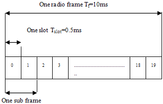 | Figure 1. Type I frame structure FDD of LTE |
Since physical layer is used in LTE, entire channels are called as LTE physical channels. In LTE, uplink channels use SC-FDMA and downlink channels use OFDMA as the multiple access technique. Even though TDMA and FDMA are available, it does support only TDD or FDD frame structure. To satisfy both frame structures of LTE, OFDM is used. However, by this way only one user can access the network. To support multi users, a new multiple access technique has been introduced by OFDM named as OFDMA. Similar to this, LTE offers a diversity technique which mitigates the effect of fading in the name of Multi Input and Multi Output. In this paper, SISO architecture for downlink PBCH is synthesized with its specifications. The results for PBCH transmitter and receiver architectures are shown by different performance methods like resource utilization, power consumption. These performances are computed by simulation followed by implementation in FPGA. One of the recent series of Virtex i.e., Virtex-5 is adopted for this paper. This paper achieves the delay of 8.216 ns for transmitter and 11.542 ns for receiver in Virtex-5 FPGA. In this paper, existing methods are explained in section 2; section 3 describes the functions and necessity of each downlink data channels; section 4 explains about the system model such as basic building blocks of transmitter and receiver of this work; section 5 describes about proposed transmitter and receiver architectures of PBCH-SISO, section 6 shows the simulated and implemented results of this proposed method.
2. Existing Work
In earlier cases, the architecture of PDSCH was discussed with its own transmitter and receiver. Synthesis and implementation of that architecture was done on Xilinx 8.1i with spartan-3E specification. After implementation the utilized devices for transmitter and receiver were tabulated[2]. Performance of LTE control channels were analyzed in[3]. Performance of LTE in terms of bit rate and average throughput were discussed in[4]. With 10 MHz bandwidth, 150Mbps peak bit rate in downlink and 40Mbps peak bit rate in uplink were achieved in[4]. LTE link layers were analyzed and link layer protocols were optimized to support higher layers in terms of low delay and low overhead[5]. Two different technologies such as WiMAX and LTE were compared in terms of spectral efficiency and radio performance in[6]. Comparison were taken by MIMO 2x2 transmit diversity and MIMO 2x2 spatial multiplexing techniques and it excluded SISO technique and it proved that LTE has low overhead than WiMAX technology[6]. Performance of LTE cellular technology like adaptive modulation and user multiplexing were discussed[7] .To satisfy the BER requirement, adaptive modulation and coding techniques were selected to maximize the spectral efficiency[7]. The current scenario of LTE faces the problem of an optimized architecture for its scalable bandwidth (1.4 MHz to 20 MHz). So this paper tries to provide architecture for SISO transmission technology for initial bandwidth (1.4 MHz) of LTE by VLSI technology. This paper is concluded with the power estimation, resource estimation and RTL schematic for proposed architecture.
3. Downlink Data Channels
In this section the significance of each downlink data channels is discussed briefly. Physical Downlink Shared Channel PDSCH is used for high data rate applications[2]. Since there are no separate channels for transforming the paging messages in LTE, this channel is used as a paging channel. This channel is shared with the operation of the other data channels such as PBCH and PMCH. It is very much used to carry the multimedia data also. Physical Broadcast Channel (PBCH) is used to carry the data to all users within the coverage area. This data are classified into two categories such as Master Information Block and System Information Block. In first case, limited number of users can access the information. In the latter case, the data are multiplexed for unicast applications. PBCH is used to carry the system information to all mobile devices. Physical Multicast Channel (PMCH) is used for the multimedia data transport. To support MBSFN subframes this channel is preferred. Also it is used to perform the MBMS in an efficient manner.
4. System Model
Physical channel processing steps for transmitter and receiver for all channels are shown in Figure 2 and in Figure 3.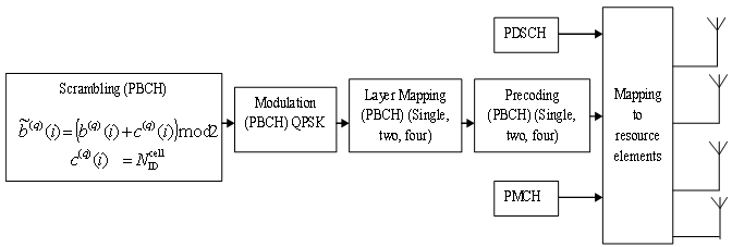 | Figure 2. System Model of PBCH at Transmitter |
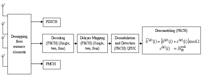 | Figure 3. System Model of PBCH at Receiver |
4.1. Physical Channel Processing Steps at Transmitter
At the transmitter side, the incoming data has to be reformed by the processes of scrambling, modulation, layer mapping, precoding and mapping to resource elements. Functionality of every module is discussed in this section.
4.1.1. Scrambling
To make the information as an unintelligible code, this scrambling module has been used. Here bit by bit scrambling is done which makes it difficult to find the original data by the intruder. Scrambling is done by using equation (1). | (1) |
where  is the original information and
  is the initialization vector which differs for every channel.
 for PBCH is defined by equation (2)
 | (2) |
4.1.2. Modulation
LTE supports various modulation techniques such as BPSK, QPSK, 16 QAM and 64 QAM. Downlink data channels use all the modulations offered by LTE but BPSK. Channel PBCH uses QPSK and other two channels are using QPSK, 16 QAM and 64 QAM modulation schemes[1]. Modulation process is done by using the multiplexers. The scrambled sequence is then modulated to create a block of modulated symbols. The scrambled bits are stored in a shift register. In QPSK modulation, pairs of bits are mapped to complex valued modulation symbols I + jQ and hence every pair of bits is converted to 16 bit complex modulated symbols in the case of QPSK.
4.1.3. Layer Mapping
Two different techniques are used in LTE layer mapping namely transmitter diversity and space diversity. The complex-valued modulated data are mapped to the higher layers such as single, two and four layers. In this paper, layer mapping is done by using the SISO technique. In MIMO or MISO cases, PBCH data can be mapped either to two layers or to four layers. It must be a single layer in the case of SISO.
4.1.4. Precoding
In this method, precoder gets the input from the layer mapper and produces the vector. This precoding is also done in single, two and four antenna cases. Precoding for single antenna case is defined by the equation (3)[1]. | (3) |
where x (i) denotes the output of the layer mapper and y(i) denotes the output of the precoder[1]. If transmitter diversity is chosen, the equations for two and four antenna cases are used as in[1]. Precoding for SISO i.e., single antenna does not require any diversity technique.
4.1.5. Mapping to Resource Elements
In this module the precoded vectors are mapped to the position of its data field in the predefined grid structure of LTE[8]. Grid structure of LTE has been constructed with 10 subframes of 2 slots each. Each slot has 14 columns and 72 rows[8]. To estimate the position of the data field, rows and columns have to be estimated initially. Counters are used for this purpose.
4.2. Physical Channel Processing Steps at Receiver
Physical channel processing steps for the receiver side are discussed by using Figure 3. In this section each block is explained in a detailed manner.
4.2.1. Demapping from Resource Elements
By knowing the position of data in the grid structure the receiver can easily get back the input of the transmitter. To estimate the position, the receiver also has to find the row and column. Similar to the mapping to resource element module, this module also consists of counters to achieve the row and column estimation.In general, counters make this massive task easier. Also control signals for each channel’s data have to be used. The enabled control signals of the particular channel indicate the presence of that channel’s data. Otherwise the designer concludes that there is no data available for that channel[8].
4.2.2. Decoding
In Demapping from resource element module, the resultant bit is passed to the decoder as an input. In the decoder the data has to be decoded using the same antenna case as chosen by the transmitter. Real and imaginary parts of the data estimation are necessary.
4.2.3. Delayer Mapping
The decoded data are then delayer mapped for all the antenna possibilities. After delayer mapping a single layer will be the output for all antenna cases by merging all the layers. This single layer resultant is given to the demodulator.
4.2.4. Demodulation
To remove the complex valued data, demodulation has to be done at the receiver side. The demodulation scheme which was used in transmitter side should be properly chosen by the receiver. The available demodulation scheme for PBCH is QPSK. Demodulation process detects the approximate data by hard decision method. This process is carried out for single, two and four antenna separately. For every decision the output bit would be a pair of bits since it is a QPSK demodulation method.
4.2.5. Descrambling
Input data became an unintelligible code by the transmitter. To get back the original data the receiver has to use same gold sequence generation. Here bit by bit descrambling technique is used.
5. Proposed Architectures
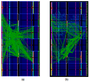
In this section the architectures of transmitter, channel and receiver are explained in Figure 4(a), (b) and in (c).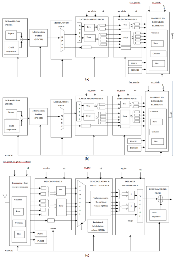 | Figure 4. Architecture of Downlink Data Channels (a) Transmitter (b) Channel (c) Receiver |
5.1. Transmitter Architecture
The overall transmitter architecture for the downlink data channel is shown in Figure 4 (a). First, the incoming codeword is Ex-Or ed with the gold sequence. The gold sequence is generated by using pseudo random sequences x1 and x2. x1 sequence is default for every channels whereas x2 sequence is application-specific and unique for each channel. These gold sequence generations are different for each channel as said in section 3. Then the scrambled bits are modulated by the modulation scheme employed at the each channel. Then the modulated stream of bits are layer mapped based on the number of antenna ports used. Layer mapping is the process of splitting stream of bits into layers based on the number of antenna ports and type of transmitter diversity used. The layer mapped output is fed as input to precoder.The precoder converts the layer mapped vector into a single precoded vector when one antenna is employed and two precoded vectors when two antennas are used. Then parity bits are added to ensure the robustness to error. The parity added precoded output is given as input to mapping to resource elements. In mapping to resource elements the data are placed on their corresponding positions.
5.2. Receiver Architecture
After transmitter but before receiver channel has to be estimated by using channel coefficients as shown in Figure 4 (b). These coefficients are calculated using 8 point FFT which are estimated for all rows of LTE grid structure irrespective of columns and slots. The scenario of the overall receiver architecture for downlink data channels is shown in Figure 4 (c). This architecture explains several blocks. Each of them refers to the reversed operation of separate modules which were done on the transmitter side. Progress starts with the step of demapping from resource elements. To do this module some control signals are required. Each control signal represents each channel in LTE grid structure. From the decoded data, the layer which was used in the transmitter side has to be selected. Here all the parity bits are removed from the resultant bit.Then all the layers are combined in receiver side. After combining the resultant data are going to be demodulated. The proper demodulation scheme should be selected in the receiver side also. By using the same gold sequence which was used in transmitter side, the original data are recovered back from the receiver.In Figure 4 (a), (b) and (c) common clock signal is also used. Since the tool Verilog provides concurrent operation, this would be the best way of reducing the clock period of every module. During implementation, internal clock is given by choosing the appropriate pin location in PlanAhead 13.2. In this paper, both architectures are done as per the Figure 4 (a), (b) and (c) and the results are shown in the next sections.
6. Results and Discussions
Simulation and implementation were done by considering some assumptions among many LTE specifications. These assumptions are illustrated in Table 1[2]. The implementation of transmitter and receiver is done on the PlanAhead 13.2 virtex-5, xc5vlx50tff1136-1 Device.| Table 1. Assumptions for downlink PBCH channel |
| | Parameter | Assumptions | | Channel Bandwidth (MHz) | 1.4 | | Number of Physical Resource Blocks (PRB) | 6 | | Cyclic Prefix | Normal | | Number of OFDM symbols per sub frame | 14 (7 in each slot) | | Frame Structure | Type I (FDD) | | Modulated bits | 16 |
|
|
Clock signal can be given internally by assigning a specified pin pattern. The hardware description language HDL used is Verilog HDL. PlanAhead 13.2 is used to perform the Verilog HDL compilation and FPGA configurations.
6.1. Simulation Results
In this paper the modules at the transmitter side which are explained in section 4 are done. The simulation result of the transmitter of downlink PBCH channel is shown in Figure 5. Clock, reset, antenna selection and transmitter diversity are the major inputs for the simulation. Transmitter can send the information if reset is disabled. If the variable ‘reset’ is enabled, all the channels are setting for their initial value again. In this case LTE grid structure starts from 0th row, 0th column and 0th slot. PBCH uses only QPSK modulation, so there is no need of modulation selection while others require it. Antenna selection variable “as_pbch” is used for the selection of PBCH antenna cases (00-disabled, 01-single, 10-two and 11-four antenna cases). As per the equation (2), additionally one clock is generated for this channel with respect to the input clock signal. According to that clock signal other modules get simulated.There is no assurance of the same antenna selection for all channels at the same time. In this paper all the possibilities of antenna selections and corresponding grid structures are generated in an optimized manner. “transmit_0”, “transmit_1”, “transmit_2”, “transmit_3” are the outputs of the grid structure. After mapping to resource elements the resultant bit is multiplied by the channel coefficients by taking 8-point FFT. These channel coefficients are estimated for all rows starting from 0 to 71 in the grid structure. Here bit by bit scrambling is done. But QPSK modulation needs 2 bits; hence buffer is used to store the previous output of scrambler. As in modulation, layers are mapped to single, two or four layers. If single layer is chosen, the output of modulation is directly mapped; otherwise buffers are required. These buffers are shown in Figure 5. Mapping to resource element grid also depends on antenna selection variable. If four antenna case is selected, then all the grid structures (transmit_0, transmit_1, transmit_2 and transmit_3) are mapped and two grid structures for two antenna case (transmit_0, transmit_1) and single (transmit_0) for single antenna case. Depending upon antenna selection, the channel estimation varies.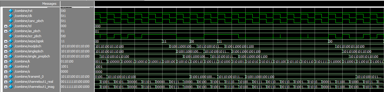 | Figure 5. Simulation result of transmitter of downlink PBCH |
 | Figure.6. Simulation result of receiver of downlink PBCH |
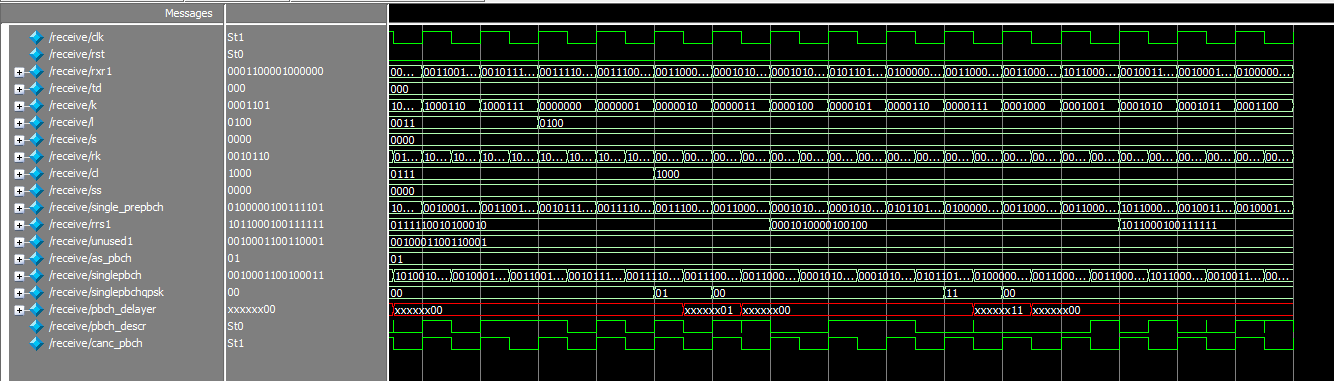
Simulation result of PBCH at receiver side is shown in Figure 6. Demapping from resource elements, decoding, demodulation (detection), delayer mapping and descrambling results are shown in Figure 6. Process starts with the channel de-estimation process. Output of this module is passed to the grid structure. Again based on row, column and slot counters, the data which are mapped to the grid at the transmitter side are retrieved at its corresponding location. Totally 7 registers for PBCH are retrieved (single antenna-1, two antenna-2 and four antenna-4). Hence seven variables are used for demapping from resource elements module.Then decoding is done based on “as_pbch” and “td” for all antenna possibilities. Then demodulation is performed by the decision-taking module in such a way that the incoming bits from the decoder have to be compared with the predefined QPSK modulation value. Then the value nearer to the appropriate value is considered as the detected value (2 bits) by the receiver. Then the detected values are delayer mapped.This proposed method advances with the existing work[2] in terms of delay and device utilization. In transmitter side, scrambling is done in the way of bit by bit method but descrambling is not performed similar to transmitter. Because of QPSK demodulation, descrambling is done using 2 bits at a time by folding method. To do this, gold sequence generation is also varies at transmitter and receiver but values of both generation remains same. Instead of generating 1 bit, receiver has to generate the gold sequence as of 2 bits to Ex-Or with the QPSK demodulated output. Basically delayer mapper concatenates the output as a single layer in the receiver side. But in SISO case, there is no need of concatenation. So delayer mapper produces the output as 2 bits because of QPSK demodulation. Here Ex-Or operation is done between gold sequence and delayer mapped output using 2 bits. Finally the data becomes intelligible to the user.
6.2. Implementation Results
Simulated program is generally used to check the architecture design with its flow and it is a virtual environment for real time applications. So implementation is needed to know about the real time applications. Simulated program is implemented on PlanAhead 13.2 Virtex-5, xc5vlx50tff1136-1 board. This board is useful to estimate the RTL design, power estimation and resource utilization briefly. FPGA editor is established to know about the routing between the input variables with the output variables. During implementation SISO technology of PBCH transmitter and receiver take 8.216 ns and 11.542 ns respectively. But simulation takes excess delay compared with implementation. The delay taken by PBCH SISO transmitter is 90.100 ns and receiver is 110.100 ns respectively. Hence implementation achieves less delay compared with simulation.
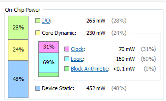
6.2.1. Power Estimation
PlanAhead board is also used to estimate the needed power for I/O devices, clock signals and logic signals. Figure 7 and Figure 8 show the power estimation for downlink PBCH transmitter and receiver. Power consumed by I/O blocks of transmitter is 133mW which is 11% of the on-chip power, power consumed by the dynamic core at transmitter is 597mW and power taken by device static is 453mW as shown in Figure 7. 265mW for I/O, 230mW for core dynamic, and 452mW for device static are consumed by PBCH receiver as shown in Figure 8.
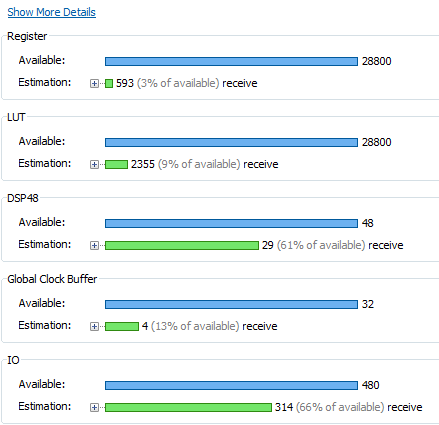
6.2.2. Resource Estimation
Resource utilization of PBCH for transmitter and receiver are shown in Figure 9 and Figure 10. These graphs include the devices like registers, LUTs (Look-Up Table) and IOs. Registers utilized by transmitter and receiver of PBCH are 481 and 593 correspondingly. Transmitter uses 8342 LUTs and 42 IOs and receiver uses 2355 LUTs and 314 IOs.
6.2.3. FPGA Editor
Routing between input and output in terms of connection is shown by FPGA editor. Figure 11 (a) and Figure 11 (b) illustrate the FPGA editor of PBCH transmitter and receiver.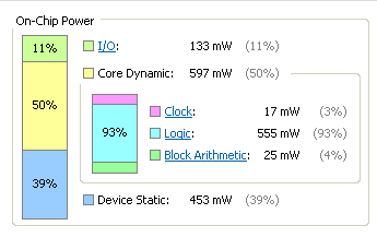 | Figure 7. Power estimation of downlink PBCH-Transmitter |
 | Figure 8. Power estimation of downlink PBCH-Receiver |
6.2.4. RTL Design
RTL design of downlink PBCH channel transmitter and receiver are shown in Figure 12 and Figure 13. Figure 12 shows scrambling module to the channel estimation module and Figure 13 shows the channel de-estimation module to the descrambling module. By clicking on the particular module the utilized resources are clearly viewed by the designer.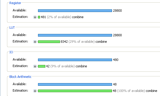 | Figure 9. Resource estimation of downlink PBCH-Transmitter |
 | Figure 10. Resource estimation of downlink PBCH-Receiver |
 | Figure 11. FPGA editor of downlink PBCH (a) Transmitter (b) Receiver |
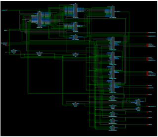 | Figure 12. RTL design of downlink PBCH-Transmitter |
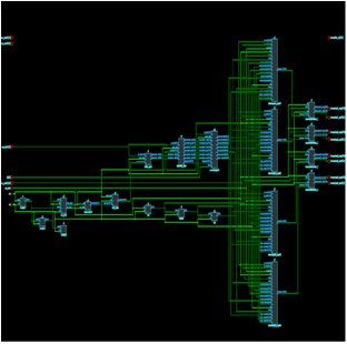 | Figure 13. RTL design of downlink PBCH-Receiver |
6. Conclusions
In this paper, an optimized architecture of downlink PBCH SISO with transmitter and receiver which include scrambling, modulation, layer mapping, precoding and mapping to resource elements and demapping from resource elements, decoding, delayer mapping, demodulation and descrambling were done and implemented on PlanAhead tool and Virtex-5 kit. The summary of power estimation and resource estimation were discussed with RTL schematic. These results will be used to enhance the performance of future work such as MISO and MIMO technologies. Power and resource utilization are further reduced by using VLSI DSP techniques.
References
| [1] | 3GPP TS 36.211: "Evolved Universal Terrestrial Radio Access (E-UTRA); Physical Channels and Modulation (Release 8)”. |
| [2] | Abbas, S.S.A. Sheeba, P.A.J. Thiruvengadam, S.J. “Design of downlink PDSCH architecture for LTE using FPGA”, in Recent Trends in Information Technology (ICRTIT), 2011 International Conference ,Chennai, Tamilnadu, June 2011. |
| [3] | S. J. Thiruvengadam, Louay M. A. Jalloul, “Performance Analysis of the 3GPP-LTE Physical Control Channels,” EURASIP Journal on Wireless Communications and Networking, vol.2010, Article ID 914934, 10 pages, Nov.2010. |
| [4] | David Martin-Sacristan, Jose F.Monserrat, Jorge Cabrejas-Penuelas, Daniel Calabuig, Salvador Garrigas and Narcis Cardona “On the way towards Fourth-Generation Mobile: 3GPP LTE and LTE-Advanced” EURASIP Journal on Wireless Communications and Networking, vol.2009, Article ID 354089, 10 pages, Jun.2009. |
| [5] | Anna Larmo, Magnus Lindstrom, Michael Meyer, Ghyslain Pelletier, Johan Torsner, Henning Wiemann and Ericsson Research “ The LTE Link-Layer Design” IEEE Magazine, April 2009. |
| [6] | Carsten Ball, Thomas Hindelang, Iavor Kambourov, Sven Eder “Spectral Efficiency Assessment and Radio Performance Comparison between LTE and WiMAX” Personal, Indoor and Mobile Radio Communications, IEEE Symposium Sep. 2008. |
| [7] | Juan J.Sanchez, D.Morales-Jimenez, G.Gomez, J.T. Enbrambasaguas “Physical Layer Performance of Long Term Evolution Cellular Technology” partially supported by the Spanish Government and the European Union under project TIC2003-07819 (FEDER) and by the company AT4W (former CETECOM, S.A.). |
| [8] | http://paul.wad.homepage.dk/LTE/lte_resource_grid.html |
 Abstract
 Reference
 Full-Text PDF
 Full-Text HTML