-
Paper Information
- Paper Submission
-
Journal Information
- About This Journal
- Editorial Board
- Current Issue
- Archive
- Author Guidelines
- Contact Us
Journal of Laboratory Chemical Education
p-ISSN: 2331-7450 e-ISSN: 2331-7469
2025; 13(2): 37-46
doi:10.5923/j.jlce.20251302.02
Received: Sep. 23, 2025; Accepted: Oct. 16, 2025; Published: Nov. 14, 2025

A Joint Adventure to Introduce Atomic Force Microscopy During “Experimenta con PREM” Summer Camp for High School Students
Stanislav Leesment 1, Marko Surtchev 1, Oleg Butyaev 1, Anamaris Meléndez 2, Melvin De Jesús 3, Idalia Ramos 2, Rolando Oyola 3
1Surfmera America Inc., 5861 Kyrene Rd, Tempe, 85283, AZ USA
2Department of Physics and Electronics, University of Puerto Rico at Humacao, Humacao, 00792, Puerto Rico, USA
3Department of Chemistry, University of Puerto Rico at Humacao, Humacao, 00792, Puerto Rico, USA
Correspondence to: Rolando Oyola , Department of Chemistry, University of Puerto Rico at Humacao, Humacao, 00792, Puerto Rico, USA.
| Email: |  |
Copyright © 2025 The Author(s). Published by Scientific & Academic Publishing.
This work is licensed under the Creative Commons Attribution International License (CC BY).
http://creativecommons.org/licenses/by/4.0/

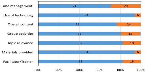
“Experimenta con PREM” (meaning “Let’s Experiment with PREM”) is a two-week summer research program at the University of Puerto Rico for high school students (HS). Experiment with PREM showcases materials science as an inclusive discipline that covers diverse interests and competencies, including materials characterization, device fabrication, soft matter, crystallography, and both experimental and theoretical-computational approaches. Within this context, atomic force microscopy is one of the most valuable techniques for characterizing nanomaterials. For the 2025 summer camp, Surfmera America Inc. partnered with the University of Puerto Rico at Humacao to offer AFM experiences to high school students. The students prepared their AFM probes, characterized a surface with a bit pattern similar to a compact disk, and performed nanolithography. After completing the experimental acquisition, the students prepared a report that included a theoretical background and surface image analysis. A student survey reveals great satisfaction with the AFM experience. This partnership proved to be an enhanced experience for the future STEM students' development.
Keywords: AFM, Laboratory Experience, Materials Education
Cite this paper: Stanislav Leesment , Marko Surtchev , Oleg Butyaev , Anamaris Meléndez , Melvin De Jesús , Idalia Ramos , Rolando Oyola , A Joint Adventure to Introduce Atomic Force Microscopy During “Experimenta con PREM” Summer Camp for High School Students, Journal of Laboratory Chemical Education, Vol. 13 No. 2, 2025, pp. 37-46. doi: 10.5923/j.jlce.20251302.02.
Article Outline
1. Introduction
- A summer research program for high school (HS) students, from grades 10 and 11, has been organized since 2005 by the NSF-funded program, UPR-PENN Partnership of Research and Education in Materials, at the University of Puerto Rico at Humacao [1]. The program name “Experimenta con PREM” (ECP, Spanish acronym), includes a week of immersion in hands-on laboratory experiences. Generally, participation in summer STEM programs as early as possible enhances the likelihood of pursuing a STEM career [2]. In addition, these early-career research experiences in STEM offer students the opportunity to engage in genuine scientific research, thereby exposing them to the work and perspectives of STEM researchers [3]. For many years, these activities have been successfully targeted at undergraduate students, as evidenced by the NSF-sponsored Research Experiences for Undergraduates (REU) programs [4].Materials Science offers an ideal environment for high school research experiences due to its highly interdisciplinary and collaborative nature. It welcomes researchers with a diverse range of skills, including theoretical, computational, experimental, engineering, synthesis, and characterization. The creation and analysis of new materials, the immediate visibility of applications, and the experience of teamwork are key features of the discipline, which help guide HS students toward nanomaterials specifically and STEM disciplines in general. Expanding access to research opportunities has been recognized as a crucial strategy for diversifying the STEM pipeline [5,6]. Therefore, initiatives to provide STEM research experiences to these students are essential. The ECP program is designed to mirror the comprehensive experience that students encounter in a REU Summer Program, spanning from the initial application to the presentation of their research findings. This year, Surfmera America Inc. joined efforts with ECP by providing one of the research experiences to HS students. Surfmera America Inc. is a company specializing in AFM instrumentation for cutting-edge nanoscience and nanotechnology research. AFM enables 3D surface topography imaging at nanometer resolution and measures surface properties, including roughness, grain size, and step heights. AFM is a fundamental technique used in Materials science (studying thin films, polymers, and nanomaterials), Biology (imaging cells, membranes, proteins, and DNA without staining or fixation), Chemistry (in investigating surface reactions and functionalization), and Physics (understanding surface forces, mechanical properties, and nanoscale phenomena). AFM isn’t just for imaging; it can measure mechanical properties (e.g., stiffness, adhesion), electrical and magnetic properties (with conductive or magnetic AFM modes), and chemical mapping (via force spectroscopy or functionalized tips). Unlike electron microscopy, AFM operates in ambient, liquid, or vacuum environments and is non-destructive, making it crucial for biological or soft samples. Proficiency in AFM is highly valued for careers in nanotechnology, biomedical research, the semiconductor industry, surface science, and engineering. For all these reasons, AFM remains a fundamental technique in nanomaterials science and is relevant for developing the next generation of scientists. Some teaching approaches have been designed to expose students to AFM and provide them with experiences in AFM, either through simulations or basic instrumental models [7]. One of the significant obstacles to exposing the students to AFM is the cost of the instrument and its availability. [8-10] In this regard, simulations and cost-effective instrumentation have been proposed. [8,10-14].Among an extensive product line, Surfmera America Inc. offers the AFM model Spark, a multi-purpose research tool that is also an ideal instrument for educational purposes. Spark can work with standard AFM cantilevers, but it can also use other cantilevers made of etched tungsten wire. This reduces the microscope's operating costs, a significant advantage when it is used for educational purposes. Spark is a compact, robust AFM designed for small samples (up to 12 mm). It features key techniques such as Amplitude Modulation AFM, Electrostatic force microscopy (EFM), Magnetic force microscopy (MFM), Kelvin probe force microscopy (KPFM), and various spectroscopic modes. This work describes the 2025 summer research experience for HS students that resulted from the partnership between ECP at the University of Puerto Rico at Humacao (UPRH) and Surfmera America Inc. Scientists from Surfmera America Inc. travelled to UPRH and participated in the ECP summer research program. The experience was programmed for a four-hour laboratory session and 3 hours to write a report. The experiment introduces the concepts of AFM microscopy, optical magnification, nanolithography, and surface analysis. These topics are relevant because the HS students lacked prior knowledge of the basic principles of AFM. We recognized that a day-long workshop does not make an expert in AFM, but for HS students, sparking the young generation's interest in the nanoworld is worth it. We also present the findings from a survey of the research experience. Altogether, the partnership complements ongoing efforts to provide HS students with access to nanoscience via AFM.
2. Materials and Methods
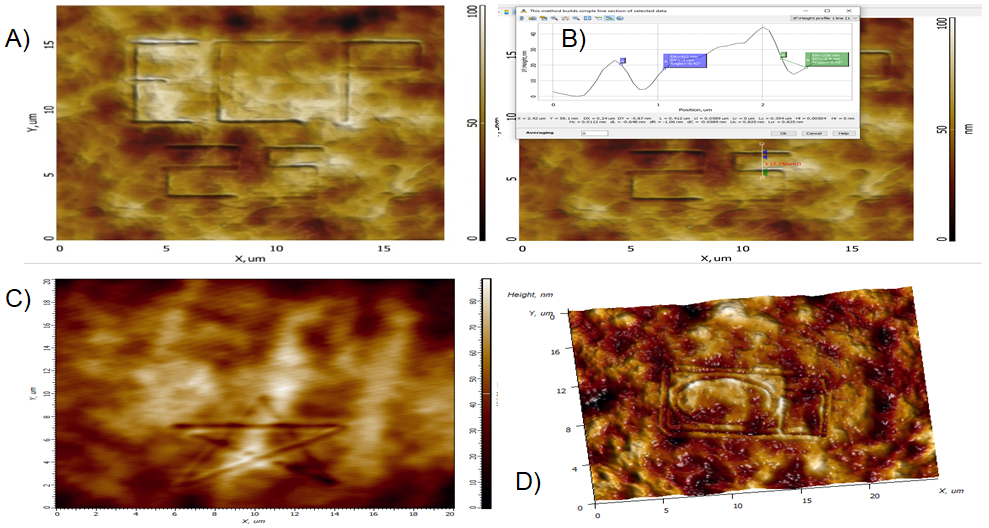
- The students prepared the AFM probes by etching a tungsten (W) wire in 10% KOH (w/w) using an etcher [13,15]. The KOH was transferred to a petri dish and placed on the etcher to create a small meniscus around the “ring,” where the W wire was sharpened by applying a constant voltage of 5V. The etcher features a built-in camera connected to a computer to display the tip-formation process. In this way, the students grasp the idea of how the tip is formed. After sharpening, the tip was transferred to the AFM Spark instrument to measure the surface, consisting of a bit pattern similar to a compact disc, using amplitude modulation mode. [12] In the second part of the experiment, the students used nanolithography to create the group team logo or any suggested image [16]. The nanolithography was performed on a high-density polyethylene sample. All data acquisition and image analysis were performed using proprietary software (Surfmera America Inc.). The overall workshop took approximately seven hours; therefore, organization, clear instructions, and continuous mentoring follow-up are essential to fulfill the objectives. Moreover, the required time for the workshop imposes a strict allocation of time.
3. Results and Discussion
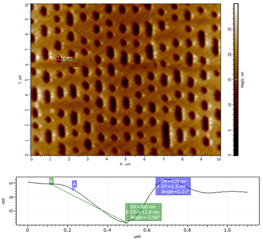
- High school students should be exposed to AFM because it fosters curiosity, develops future skills, links science to real-world innovation, and prepares the next generation of scientists. Observing how AFM is used to design better batteries, medical devices, or drug-delivery systems helps students connect science to real-world impact. AFM experiences introduce students to real nanotechnology, not just textbook science, and help them understand how scientists perceive atoms and molecules, sparking interest in research and STEM careers. Moreover, hands-on AFM experience enables students to visualize and understand the nanoscale, where many materials exhibit distinct behaviours. In this way, students recognize that tiny changes at the nanoscale can have a significant impact on how materials function (e.g., in electronics, biology, or medicine). Thus, introducing students to AFM at an early stage is essential because it provides nanoscale-level insight into the structure, properties, and behaviour of materials. In summary, learning AFM opens doors to cutting-edge research and technological innovation, equipping the students with the tools to explore and manipulate the world at the nanoscale.The experiment begins with a brief introduction to microscopy and magnification. The diffraction limit was introduced as the limiting factor of optical magnification to characterize nanomaterials. Thereafter, the introduction of scanning electron microscopy (SEM) was presented to establish the requirement to measure nanoscale materials. The pros and cons of SEM are first discussed, followed by a discussion of AFM principles and experimental procedures. A brief experimental procedure is presented to help students understand the basics of measuring an AFM image. Afterward, the hands-on experience starts by preparing the probe tip by etching a tungsten (W) wire in KOH (10% w/w) with an etcher.The students then measured the topography of the provided sample, which consisted of a bit pattern like that of a compact disc. Figure 1 shows an example of the obtained topography image by one of the student groups. A clear surface pattern with an oval form, characteristic of a bit sequence, is observed. Image analysis was performed using the proprietary software. For example, the green line shown in Figure 1 yields a bit width and depth of 418 and 13.6 nm, respectively.
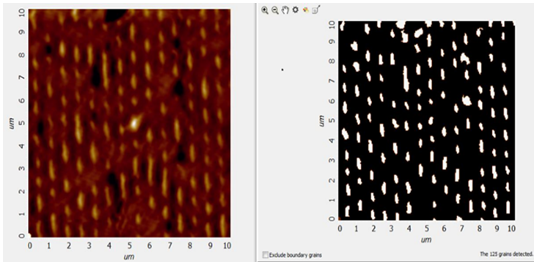 | Figure 2. Grain analysis of the CD surface. Inverted topography (left) and the detected grains/holes (right) |
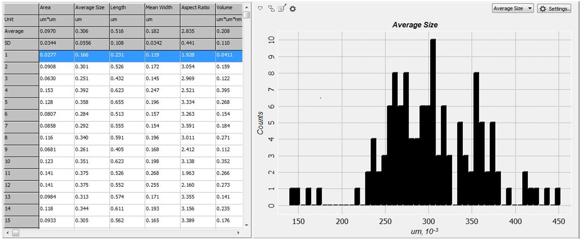 | Figure 3. The results from the Grain analysis are presented in a table with data for each grain/hole, as well as in a histogram |
4. Conclusions
- During the laboratory research days of the ECP2025 summer camp, HS students had the opportunity to participate in a laboratory offered by Surfmera America Inc., an international company based in Arizona that specializes in the development of advanced scientific technologies in partnership with the UPR-Humacao. Surfmera America Inc. scientists travelled to UPR-Humacao to provide HS students with the experience of using a compact AFM (Spark model), which enabled them to visualize materials at the nanoscale, a key observational level in modern materials research. This activity exemplifies how collaboration between industry and academia can open doors for young people to access cutting-edge technology and experience the highest level of science. Moreover, it provides a sparkling experience of the nano-world for HS school students, which is difficult to achieve under normal conditions.
 | Supplementary Material: Post-Workshop Survey |
ACKNOWLEDGEMENT
- This work was supported by NSF-DMR-2122102, NSF-MRI-2320039, and Surfmera America Inc. (Tempe, AZ, USA)
DISCLOSURE
- The authors declare no competing financial interest.
 Abstract
 Reference
 Full-Text PDF
 Full-text HTML