-
Paper Information
- Paper Submission
-
Journal Information
- About This Journal
- Editorial Board
- Current Issue
- Archive
- Author Guidelines
- Contact Us
Journal of Laboratory Chemical Education
p-ISSN: 2331-7450 e-ISSN: 2331-7469
2019; 7(3): 45-49
doi:10.5923/j.jlce.20190703.01

Healable Layer-by-Layer Assembled WO3-Polymeric Composite Films: Undergraduate Experiments for Nanomaterials
 Abstract
 Reference
 Full-Text PDF
 Full-text HTML
Yingxi Lu 1, Hongkun Yang 1, Wenhui Wu 2, Xu Zhang 1, Huijuan Yue 3, Yuhan Wei 2, Dan Xue 2, Ning Sui 1, Xianfeng Zhou 2, Fanglin Du 1
1College of Materials Science and Engineering, Qingdao University of Science and Technology, Qingdao, P.R. China
2College of Polymer Science and Engineering, Qingdao University of Science and Technology, Qingdao, P.R. China
3State Key Laboratory of Inorganic Synthesis and Preparative Chemistry, College of Chemistry, Jilin University, Changchun, P.R. China
Correspondence to: Yingxi Lu , College of Materials Science and Engineering, Qingdao University of Science and Technology, Qingdao, P.R. China.
| Email: |  |
Copyright © 2019 The Author(s). Published by Scientific & Academic Publishing.
This work is licensed under the Creative Commons Attribution International License (CC BY).
http://creativecommons.org/licenses/by/4.0/

Healable WO3-polymeric composite films were fabricated by a simple method of layer-by-layer (LbL) assembly technique. The assembled films can heal damages such as scratches and cuts for multiple times on the same location by simply exposure to an acidic solution (pH 2.5). The healability was examined by UV-vis spectrophotometer. The surface morphology and composition of the films were characterized by atomic force microscopy (AFM), fourier transform infrared (FT-IR) spectrophotometer and X-ray powder diffraction (XRD).
Keywords: Layer-by-layer assembly, Healing materials, Tungsten oxide, Electrochromics
Cite this paper: Yingxi Lu , Hongkun Yang , Wenhui Wu , Xu Zhang , Huijuan Yue , Yuhan Wei , Dan Xue , Ning Sui , Xianfeng Zhou , Fanglin Du , Healable Layer-by-Layer Assembled WO3-Polymeric Composite Films: Undergraduate Experiments for Nanomaterials, Journal of Laboratory Chemical Education, Vol. 7 No. 3, 2019, pp. 45-49. doi: 10.5923/j.jlce.20190703.01.
Article Outline
1. Introduction
- Self-healing materials can heal damages with inherent materials to prolong lifetimes and improve the stability. The healing mechanism can be categorized by the nature of the reversible bonds-covalent and non-covalent [1,2]. The healing process based on the covalent bonds can be realized by the Diels-Alder cycloaddition reaction, disulfide bridges, N-O bond, et al. The driving force for healing based on the non-covalently bounds include the hydrogen-bond [3], ionic interaction [4], π-π stacking [5], metal-ligand coordination [6] and host-guest interaction [7], hydrophobic interaction [8].The compelling needs of next-generation electronics would require stretchable, foldable and even wearable electronic devices, including flexible electrochromic devices [9-11]. However, the reliability and lifespan of flexible electrochromic devices can be seriously decreased by the internal micro-cracks or partial injuries during the process of frequent stretching, folding, and screwing in practical applications. Motived by this need, we propose to introduce the concept of self-healing into the electrochromic devices for realization of its self-healing to enhance operation lifespan. In this research, inorganic/organic composite films are constructed based on the hydrogen-bond interactions by layer-by-layer (LbL) assembly technique. Tungsten oxide (WO3) is selected as the inorganic electrochromic material, which originates from the peroxotungstic acid (PTA). Poly(acrylic acid) (PAA) and poly(ethylene oxide) (PEO) are used as the film compositions. By alternatively assembling in PAA and (PTA&PEO) solutions, WO3-polymeric composite films are prepared. The development of this project will provide a feasible method to build up a self-healing, flexible electrochromic film. The goal of this experiment is to design a simple and practical procedure for preparing healable composite films. By doing this experiment, the undergraduate students understand the basic theoretical principles, the process of LbL assembly and the advanced knowledge in nanoscience. This experiment is suitable for undergraduate students in the study of general chemistry, inorganic chemistry and physical chemistry.
2. Experiment Description
2.1. Materials
- Poly(ethylene oxide) (PEO, Mw ca. 100k) and H2O2 (30 wt.%) were purchased from Alfa Aesar. Tungsten powder was purchased from Aladdin. Poly(acrylic acid) (PAA, Mw ca. 250k) and poly(diallyldimethylammonium chloride) (PDDA, Mw 100k-200k) were purchased from Sigma-Aldrich. All chemical reagents were used as received without further purification. Distilled water was used in all the experiments.
2.2. Instruments and Characterization
- The LbL deposition of composite films was conducted automatically by a programmable dipping machine (SYDC-100 M, SAN-YAN, Shanghai) at room temperature. The surface morphology was characterized by atomic force microscopy (AFM, Multimode 8, Bruker) under ambient conditions. AFM was operated in the ScanAsyst mode with an optical readout using Au-coated silicon cantilevers (SNL-10, Bruker). The film-thickness determination was carried out on a Quanta FEG 250 scanning electron microscope (SEM). The samples were coated with a thin layer of gold prior to imaging. The healing process of the composite film was tracked by a GAOPIN GP-650S optical microscopy. Optical transmittance spectra of the films were measured using a Varian Cary 500 UV-Vis-NIR Spectrophotometer. Infrared transmittance spectra were recorded with a Tensor 27 FT-IR spectrophotometer (Bruker). The crystal structure of tungsten oxide was characterized by a D/MAX-2500 X-ray powder diffractometer with Cu-Ka radiation (λ=1.5406 Å) operated at 40 kV and 150 mA.
3. Experimental Procedure
3.1. Preparation of Peroxotungstic Acid (PTA) Precursor
- Peroxotungstic acid (PTA) was used as a precursor for tungsten oxides. The PTA solution was synthesized by oxidative dissolution of tungsten powder in H2O2 according to the literature [12,13]. Tungsten powder was added into 30 wt.% H2O2 solution and stirred for 2 days at room temperature. A yellowish solution of PTA solution was obtained, which was filtered to remove non-reacted tungsten powder. A transparent and stable mixture of PTA and PEO (2 mg·mL-1, pH 2.5) was obtained, before deposition the composite films, and the mixture was noted as (PTA&PEO).
3.2. Preparation of WO3 Composite Films
- The (PAA/PTA&PEO) multilayer films were assembled on the substrates of silicon wafer or glass microscope slide by the layer-by-layer (LbL) assembly technique [14,15]. The driving force for the film assembly is the hydrogen-bonding interaction between carboxylic acid groups in PAA and ether oxygens (–C–O–C–) in PEO polymer. A newly cleaned substrate was immersed in an aqueous solution of 1 mg·mL-1 PDDA for 20 min to obtain a positive charged layer of PDDA. The (PAA/PTA&PEO) multilayer films were prepared by alternating immersion of the PDDA-modified substrates into the PAA polymer solution (2 mg·mL-1, pH 2.5) and the mixture solution of PTA and PEO for 5 min each. After each deposition, the substrates were rinsed for 1 min in acidic solution (pH 2.5) for two times. By repeating the above deposition and rinsing steps in a cyclic fashion, (PAA/PTA&PEO)*n films with desired number of deposition cycles were fabricated. The above assembly process can also be manually operated, as shown in Figure 1. The drying step with N2 flow was only conducted after depositing the last layer.
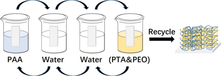 | Figure 1. Schematic illustration for the preparation of (PAA/PTA & PEO)*n multilayer films by LbL assembly technique |
4. Result and Discussion
4.1. Characterization of Synthesized PTA Precursor
- The typical XRD patterns of the as-synthesized PTA precursor and the mixture of PEO and PTA are shown in Figure 2. According to the figure, the wide peaks at 2θ ≈ 26° represent the amorphous phase formation of WO3, which are in good agreement with the literature values [12,16]. Even after mixing with PEO polymer, the amorphous phase of WO3 is not changed.
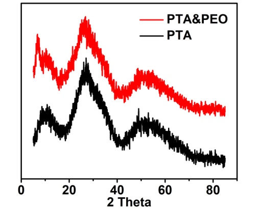 | Figure 2. XRD patterns of the powdered PTA precursor and the mixture of PEO and PTA |
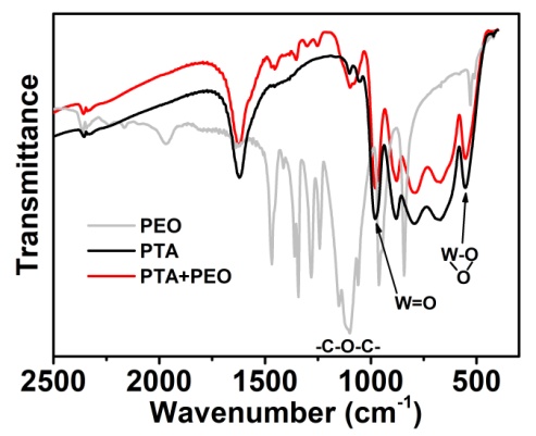 | Figure 3. FT-IR spectra of the powdered PTA, PEO and the mixture of PTA and PEO (KBr pellet) |
4.2. Surface Morphology and Thickness of Composite Films
- The surface morphology of the assembled (PAA/PTA&PEO)*60 multilayers was examined by AFM, as shown in Figure 4a. The surface roughness is 0.56 nm with scan size of 8×8 µm. The WO3 particles are uniformly distributed on the film surface and the particle size is range from 120 nm to 250 nm. The thickness of the (PAA/PTA&PEO)*60 multilayers was determined by the cross-sectional SEM, as shown in Figure 4b. The LbL-assembled (PAA/PTA&PEO)*60 film is uniform, and the thickness is about 4.2 µm.
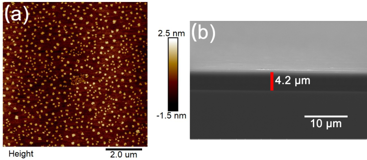 | Figure 4. (a) AFM image for the assembled (PAA/PTA&PEO)*60 multilayers on the silicon wafer. Scan size is 8×8 µm; (b) Cross-sectional SEM image of the (PAA/PTA&PEO)*60 film |
4.3. Healing Properties of (PAA/PTA&PEO) Films
- The (PAA/PTA&PEO)*60 multilayer film is colorless and transparent. As shown in Fig. 5, in the whole visible light region and near-infrared region, the multilayer film assembled on the glass slide is highly transparent, with its transmittance at 550 nm being ∼80%. The transparency of the film significantly decreased to ∼46% at 550 nm when the film was repeatedly scratched with a 800-grit sandpaper. After immersing the scratched composite film in acidic solution (pH 2.5) for 30 min, the transparency of the film is almost restored to ~75%, as indicated in Fig. 5. In the near-infrared region, the transparency of the (PAA/PTA&PEO)*60 film decreased from ~83% to ~47% at 1800 nm after scratching with the sandpaper. While the transparency of the film restores to ~77% at 1800 nm after healing in pH 2.5 water for 30 min. It is found that the further elongation of the healing time in pH 2.5 water does not improve the transparency of the (PAA/PTA&PEO)*60 film.
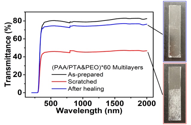 | Figure 5. UV-vis transmission spectra of the (PAA/PTA&PEO)*60 film prepared on a glass substrate before and after healing in pH 2.5 water. The correnponding digital images for the (PAA/PTA&PEO)*60 film are shown on the right |
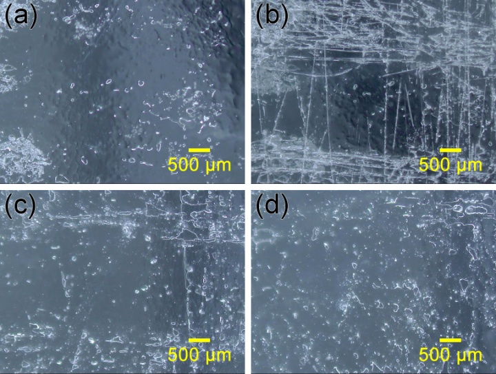 | Figure 6. Healing process of the (PAA/PTA&PEO)*60 film prepared on the glass slide. (a) original film surface; (b) film surface scratched with a 800-grit sandpaper; (c) and (d) film surface after healing in acidic solution (pH 2.5) for 5 min and 30 min, respectively |
4.4. Application of the Healable Composite Films
- These healable (PAA/PTA&PEO) composite films can be further used as an electrochromic film for preparing healable and stretchable electrochromic device, due to the existence of WO3 [19]. All the experiments are performed at room temperature and atmospheric pressure, which making them suitable for physical chemistry and materials chemistry laboratories.
5. Conclusions
- Layer-by-layer assembled (PAA/PTA&PEO) composite films based on hydrogen-bond interaction between PAA and PEO are successfully prepared. The (PAA/PTA&PEO)*60 composite film behave good healing property in acid water (pH 2.5), due to the fluidity of the polymers and reformation of the hydrogen-bonding interactions in the films. The healing process is dependent on the immersion time in acidic water and the complete healing of the scratches takes about 30 min. The incorporation of WO3 makes this healable composite films have potential applications in the field of stretchable electrochromic devices.
ACKNOWLEDGEMENTS
- This work was financially supported by the National Natural Science Foundation of China (NSFC Grant No. 21704051) and the Open Research Fund of State Key Laboratory of Inorganic Synthesis and Preparative Chemistry, College of Chemistry, Jilin University (2019-19).