-
Paper Information
- Paper Submission
-
Journal Information
- About This Journal
- Editorial Board
- Current Issue
- Archive
- Author Guidelines
- Contact Us
International Journal of Instrumentation Science
p-ISSN: 2324-9994 e-ISSN: 2324-9986
2016; 5(1): 1-5
doi:10.5923/j.instrument.20160501.01

Benchtop Semi-Automated Solid State Photolithography Tool
 Abstract
 Reference
 Full-Text PDF
 Full-text HTML
Z. Mouffak, A. Olaivar, A. N. Vang
Department of Electrical and Computer Engineering, California State University Fresno, Fresno, USA
Correspondence to: Z. Mouffak, Department of Electrical and Computer Engineering, California State University Fresno, Fresno, USA.
| Email: |  |
Copyright © 2016 Scientific & Academic Publishing. All Rights Reserved.
This work is licensed under the Creative Commons Attribution International License (CC BY).
http://creativecommons.org/licenses/by/4.0/

The cost of a lab-grade photolithography tool is typically of the order of tens of thousands of dollars, a prohibitive price for many organizations that wish to prototype the fabrication of nanostructures. The availability of a more cost-friendly implementation of photolithography is crucial to the research and development of new technologies in nanoscale devices. In this work, we built a scaled down simplified version of a patterning system, the benchtop photolithography tool, which is expected to replicate certain nanopatterning techniques for under $300 —a tiny fraction of the cost of a typical mask aligner. A semi-automated benchtop photolithography tool is designed, fabricated, and programmed for prototyping and for research purposes. We use a USB 32-Bit Whacker PIC32MX795 Development Board that drives a programmable touchscreen, a UV LED array, a shutter, and a UV sensor, allowing us to have the desired high precision UV exposure. The integration of a microcontroller to operate the peripheral components of the tool allows to automate the small-scale photolithography process.
Keywords: Benchtop photolithography, Semiconductor processing, Nanopatterning, PIC microcontroller
Cite this paper: Z. Mouffak, A. Olaivar, A. N. Vang, Benchtop Semi-Automated Solid State Photolithography Tool, International Journal of Instrumentation Science, Vol. 5 No. 1, 2016, pp. 1-5. doi: 10.5923/j.instrument.20160501.01.
Article Outline
1. Introduction
- There is an increasing demand for optimizing the tools for nanopatterning techniques in the electronics industry. Wafer patterning at the micrometer and nanometer scales is usually accomplished using photolithography, a specialized process that incorporates a significant amount of resource-intensive components, such as gas cooling lines and high-voltage power supplies. A photolithography tools is usually a bulky expensive equipment that the majority of research labs can’t afford [1]. Few attempts have been made to date to come up with a cheaper solution to this problem, including maskless lithography [2] [3], and electron beam lithography [4]. While, those are techniques meant to primarily avoid using the optical lithography due to limitations at the nanosize level, very little work has been done to fabricate a cheap tool for schools and small labs that usually only need access to micro and slightly sub-micron capabilities. Odom and Hungtinton were capable of demonstrating high resolution photolithography in the nanoscale level, using very simple out of the shelf components, resulting in a very cheap benchtop tool that shows great promise for usage in labs, and possibly manufacturing. Their tool was fully manual, consisting in an enclosed platform for which a silicon wafer is placed under an LED array and exposed to UV light for a specified amount of time [5]. Although this design is certainly a step in the right direction in making wafer patterning a more cost-friendly venture, several improvements can be made to this system. First, the duration of the UV array's “on” time can be automated using a microcontroller (rather than manually turning on the array and timing the wafer exposure using a separate timer). This minimizes any handling of the array and the wafer. Second, choosing the “on” duration and displaying any relevant data can be done using a user-friendly touch screen. Third, a shutter can be included to expose the wafer to the UV light after the UV array is turned on (rather than exposing the wafer while the UV array is in the process of turning on). Finally, the size of the closed system can be scaled down further in order to make it as benchtop-friendly as possible.
2. Design Procedure
- Figure 1 shows a picture of the benchtop photolithography tool we fabricated. The door is closed during exposure. The enclosure is a sheet metal box with hinged cover to isolate the silicon wafer from stray light entering the patterning area (Model JBH-4961-KO Steel NEMA 1 from BUD Industries). This metal box houses the UV array, motor, circuitry, and microcontroller. The UV array consists in 51 LEDs evenly distributed on a circular array taken from a 395 nm 51 UV Ultraviolet LED flashlight from Esco-Lite. Furthermore, we used an HS-422 Servo Motor, and a UBW32 – USB 32-Bit Whacker microcontroller. A shutter made from black ABS plastic was fabricated and attached to the shaft of the servo motor. The purpose of the shutter is to ensure that the wafer is exposed to UV light for a set amount of time once the LED array is turned on completely, which ensures more precision in the exposure time. In addition, the shutter provides extra protection for the silicon wafer in the event that an error occurs during the operation of the system. A shelf made from 0.75” thick plastic was used to mount the LED array above the patterning area inside the metal box. Circuit simulations (using the Multisim software) were completed to ensure that all electrical components are safely integrated into the system.
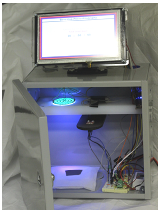 | Figure 1. The benchtop photolithography tool |
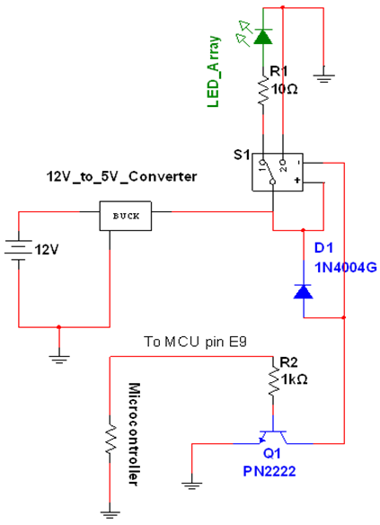 | Figure 2. Schematic of the relay and UV array |
2.1. Microcontroller and Peripheral Programming
- We used a UBW32 Bit Whacker (PIC32MX795F512L) microcontroller to interface peripheral devices [6], consisting in a 7” TFT Touchscreen with SSD1963 Graphic Driver an XPT2046 Touchscreen Driver, and an ML85 UV sensor. The concept flowchart in Figure 3 depicts each step of the photolithography process operation that the tool accomplishes. First, the microcontroller is powered and the LCD touch screen is initialized. During this step, the user inputs the light intensity and time of exposure. Afterward, the PIC32 microcontroller (MCU) will process the inputs from the LCD touchscreen and begin to set up the other components to make the system ready to receive the wafer. Once the wafer is inserted and the box is closed, the UV array turns on. The wafer will then be exposed to the UV light after the shutter is prompted to open, and the timing of the exposure time will begin. The wafer will be exposed to the UV light until the time specified has elapsed. As soon as the set timing is finished, the wafer will be covered using the shutter, and the LED will turn off. The user will be prompted that the process has completed and can then remove the wafer.
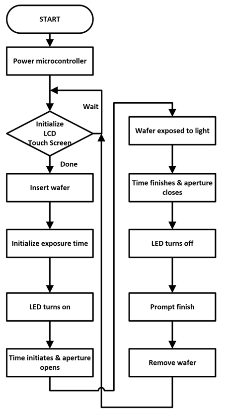 | Figure 3. Block diagram of programming process |
2.2. Hardware Implementation
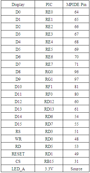
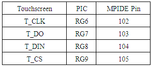
- The 7” TFT touchscreen contains two main drivers connected to the UBW32: The SSD1963 graphic driver and the XPT2046 touchscreen driver. The TFT touchscreen is connected to the UBW32 through 25 pins. The graphic driver use 21 pins and the touchscreen driver uses 4 pins. On the back of the screen, there are 40 pins (20x2). Figure 4 shows the TFT 40 pins and the UBW32. Each pin has a corresponding name, such as RB0, RE1, RF3, etc. In Table 1, the Display column shows the pinout on the TFT that is expected to connect to the PIC pin using the respective PIC column. Most of the pins on Table 1 are connected to the right side of the UBW32. Table 2 specifies the touchscreen pin that is connected to the UBW32. The touchscreen column shows the pins on the TFT and the PIC column shows the pins on the UBW32.
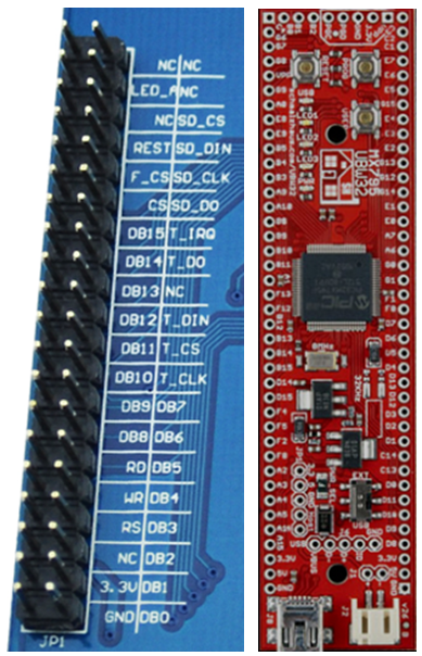 | Figure 4. TFT 40 pins (L), and UBW32 Bit Whacker (R) |
|
|
3. Software Implementation
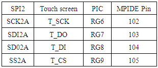
- The UBW32 Bit Whacker was installed with the PIC32-avrdude-bootloader, which provides the following easy programming using arduino similar interface and IDE, and allows the connection of a mini USB to program the UBW32. The software used to program the UBW32 is MPIDE, which is open source, and provides a large amount of documentation. This application is from chipKIT and can be downloaded [7]. The software used to program the UBW32 is MPIDE. The programming environment is the same as the Arduino IDE. ChipKit also provides an MPIDE quick start online. The most important library that is needed for this project is the DisplayCore library. This includes the SSD1963 display driver library and the XPT2046 touchscreen library, which can be downloaded online [8]. The SSD1963 display driver initialization is in the source code.The XPT2046 touchscreen driver initialization is in the source code. The touchscreen driver uses a serial peripheral interface (SPI). By default, SPI2 on the PIC32 is used when DSPI0 initializes a new SPI. The SPI data pin or SS pin is RG9 on UBW32. The rest of the SPI pinout can be found on Table 3.
|
3.1. Main loop
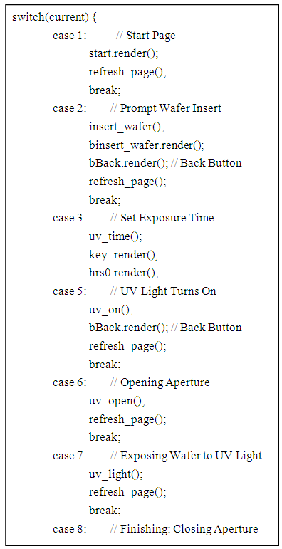
- We use an MVC (Model-View-Controller) software architecture to work with the TFT touchscreen display. Figure 5 shows the general structure of the MVC program used for the TFT. In MVC, View (display screen) stay constant until the Model (data) is updated or changed from the Control (PIC). This is implemented by using a switch statement in the main loop to control the page. A global variable called “current” is adjusted throughout the loop and changes the display of the screen. Each “case” in the switch statement corrsponds to a different step in the photolithography process. Case 1 is the startup page that prompts the user to press the START button. Once the START button is pressed, the event for the pressed button will begin and update the “current” variable to 2. When the current variable is changed to 2 and case 1 is completed, within the main loop the switch statement will move to case 2. Case 2 will execute, which updates the screen to prompt the user to insert a wafer. This process continues until the current variable reaches case 8. Once case 8 is completed, the current variable will reset to 1. When current is 1, the whole process will be ready to begin again.
 | Figure 5. General structure of the MVC program on which the TFT program works |
4. Data and Results
- The operation of the relay/UV array circuitry, 3.3 V output circuit, and servo were all proven successful. The shutter completely covered the patterning area when prompted to close, and also completely exposed the patterning area when prompted to open. The servo was shown to rotate both clockwise and counterclockwise 90 degrees to facilitate the movement of the shutter. The UV light could be driven to the “on” or “off” position using the microcontroller, and the relay allowed the light to successfully source its power directly from the output of the 12 V to 5 V step down converter. The 3.3 V output circuitry produced 3.28 V at the output of the voltage regulator, which provided a clean signal to the touchscreen. The benchtop photolithography tool was successfully programmed and automated using the UBW32 and the touchscreen. Figure 6 shows a screenshot of the keypad programmed into the touchscreen. In addition, the UV array and servo motor were successfully driven using the UBW32 and the touchscreen. The benchtop photolithography tool thus was fully functional and ready to be tested with silicon wafers.
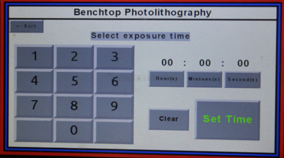 | Figure 6. Touchscreen with keypad displayed |
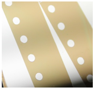 | Figure 7. A silicon sample patterned using the benchtop Photolithography tool |
5. Conclusions
- In this work, it has been possible to design and fabricate a semi-automated benchtop photolithography patterning system using a solid state UV LED array, a touch screen, and a microcontroller; a PIC32MX795 Development Board that drives a programmable touchscreen, a UV LED array, a shutter, and a UV sensor. The system, being small and extremely cheap, can help academic labs engage in research that requires material surface patterning.
ACKNOWLEDGEMENTS
- This work was done using funds of the Lyles Foundation of the Lyles College of Engineering at Fresno State.