-
Paper Information
- Paper Submission
-
Journal Information
- About This Journal
- Editorial Board
- Current Issue
- Archive
- Author Guidelines
- Contact Us
International Journal of Optoelectronic Engineering
p-ISSN: 2167-7301 e-ISSN: 2167-731X
2018; 8(1): 1-8
doi:10.5923/j.ijoe.20180801.01

The Impact of Dysprosium Ions as a Dopant on Linear and Nonlinear Optical Dispersion Parameters in a-Se Thin Film
 Abstract
 Reference
 Full-Text PDF
 Full-text HTML
Fathy A. Abdel-Wahab, Heba Abdel Maksoud
Physics Department, Faculty of Science, Ain Shams University, Cairo, Egypt
Correspondence to: Fathy A. Abdel-Wahab, Physics Department, Faculty of Science, Ain Shams University, Cairo, Egypt.
| Email: |  |
Copyright © 2018 The Author(s). Published by Scientific & Academic Publishing.
This work is licensed under the Creative Commons Attribution International License (CC BY).
http://creativecommons.org/licenses/by/4.0/

Thin films of un-doped and doped a-Se with Dysprosium rare earth ions have been prepared by thermal evaporation technique. The optical transmission spectra of the investigated films have been measured in a wide spectral range and used to calculate the linear optical constants together with the optical energy gap of studied films. The observed decrease in the values of the energy gap against the increase of the Dysprosium (Dy) content in a-Se films has been explained using Mott and Davis Model and in terms of electronegativity difference of the constituent atoms. Furthermore, the dispersion of nonlinear parameters such as second order refractive index and nonlinear absorption coefficient (two-photon absorption coefficient) of investigated films are presented and discussed.
Keywords: Dysprosium ions, Se doped Dy, Optical transmittance, Optical energy gap, Second order refractive index
Cite this paper: Fathy A. Abdel-Wahab, Heba Abdel Maksoud, The Impact of Dysprosium Ions as a Dopant on Linear and Nonlinear Optical Dispersion Parameters in a-Se Thin Film, International Journal of Optoelectronic Engineering, Vol. 8 No. 1, 2018, pp. 1-8. doi: 10.5923/j.ijoe.20180801.01.
Article Outline
1. Introduction
- Rare earth Dysprosium (Dy) ions doped glasses are very interesting due to its application as solid-state laser materials and as a suitable candidate for analysing the energy-efficient luminescent materials [1, 2]. Furthermore, as a result of presence of active f electron shell, which is very sensitive to the surrounding atoms of the host environment, in the electronic configuration of Dy it can provide an emission at 1.3 μm due to the 6F11/2, 6H9/2→6H15/2 transitions [3]. In addition, due to its absorption band at approximately 800 nm, it could be excited using a cheap commercial laser diode. In contrast, the structure of a-Se consists of flat and straight zigzag chains (Sen) and eight membered rings (Se8). This structure makes a-Se characterizes by existence of localized states in its energy gap which are created due to presence of structural dangling bond defects and absence of long range order [4-6]. Also, the structural disorder of a-Se makes it and its chalcogenide alloys to have a high thermal stability, high degree of covalent bonding, large refractive index and optical transparency in the infra-red (IR) spectral regions up to 10 μm. Furthermore, due to its high rare earth solubility, high emission quantum efficiency and the low phonon energy it could be used as a suitable host medium for Dy ions to enhance its mid-IR laser emission [7, 8]. Consequently, the investigation of the optical properties of doped a-Se with Dy ions is very important to improve the performance of Laser emission [9]. In the previous work [10], the study of Selenium films was intended to have a comprehensive understanding over the influence of Dysprosium (Dy) ion dopant on the ac conductivity and dielectric parameters of a-Se films. The present aims to gain a better investigation on the effect of doping with Dy on the optical dispersion relations of the complex dielectric constant, optical energy gap and material dispersion. Furthermore, the effect of doping of a-Se with Dy ions on second order refractive index and two photons absorption are calculated and discussed.
2. Experimental Details
- Bulk selenium samples doped with Dysprosium with ratios 0.008 and 0.01 at. % are prepared by mixing suitable proportions of Se and Dy, of purity 5 N, in a silica tube sealed at 10-5 Torr. The mixture was heated in an electric furnace up to 950°C and kept at that temperature for 9 h. The obtained bulk ingots are used as source material to prepare thin films by the thermal evaporation technique. More details about bulk and thin films preparation of Se doped Dy is given elsewhere [10]. After evaporation, the thickness of the fresh films was accurately determined by an optical interference method and is found to be in the range of 750-804 nm. The structural phase of as-prepared thin film samples has been identified using an X-ray diffraction pattern (XRD) computerized system (model: Philips EXPERT-MPDUG PW-3040 diffractometer with Cu Ka radiation source). Computer-aided two-beam spectrophotometer of type Shimadzu- 3101PC UV–VIS–NIR, is used to record the optical transmittance (T) as a function of wavelength (λ) for the investigated films. A resolution limit of 0.2 nm and a sampling interval of 2 nm were utilized for recording the different measuring points. The accuracy of measuring T(λ) is 0.003 with the incident beam at normal incidence to the film surface. The optical measurements were carried out at room temperature in the spectral region of 500–2500 nm.
3. Results and Discussion
- Figure 1 shows the recorded XRD patterns for the studied as-prepared a-Se, previous work of SeDy0.008 films [10], and the present work [P.W.] of Se films doped with 0.01 at. % with Dy. In this figure, the XRD pattern of the fresh Se films reflects its amorphous nature. The observed diffraction peaks in case of Se doped with 0.008 at. % Dy [10] means the growth of crystalline phase on the expense of amorphous state. This crystalline phase consists of mixed phases of elemental Se, Dy and tetragonal and orthorhombic structures of SeDy as shown in Figure 1. Furthermore, increasing the Dy content in a-Se up to 0.01 at. % increased the intensity of the diffraction peaks for (102) of Dy and (002), (003) and (112) phases for SeDy which means that increasing the growth of crystalline zones in SeDy0.01 as shown in Figure 1.
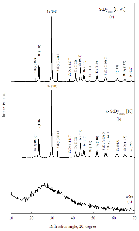 | Figure 1. XRD pattern for a-Se (a), c-SeDy0.008 [10] (b) and the present work [P. W.] of SeDy0.01 (c) thin films. It should be noted that the diffraction pattern of c-SeDy0.008 [10] is added to the figure for the sake of comparison |
3.1. Linear Optical Dispersion
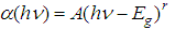
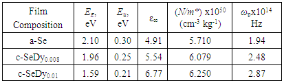
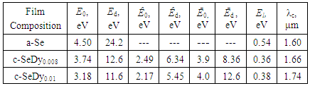
- The linear optical constants such as refractive index (n), extinction coefficient (k) and optical energy gap, Eg, are considered as a key parameter for optimizing optical properties of a given optical application [11]. The measured optical transmission against wavelength are used evaluate the linear constants n and k for un-doped and Dy doped Se films using Swanepoel method [12-14]. Figure 2 shows the dependence of the calculated linear optical constants n and k, on the applied wavelength and compositions of the investigated samples. In Figure 2, the calculated values of n and k show a decrease against wavelength which is due to the normal optical dispersion of the studied films. Indeed, the figure shows also an increase of n and k against the increase of Dy ratio in the network of a-Se. This behaviour can be interpreted as follows: due to the electronic configuration of Dysprosium [Xe] 4f106s2 each Dy atom provides a-Se network with two electrons and transform to Dy2+ ion. Consequently, an increase in the density of dipoles and electrons in Selenium network is expected as calculated in Table 1 of the present work. In Table 1 the density of dipoles increases from 5.71x1050 cm-3.Kg-1 (for a-Se) up to 6.25x1050 cm-3.Kg-1 (for c-SeDy0.01). The increased density of oscillating dipoles and its associated density of electrons increases the electronic polazibility which controls not only the refractive index but also the optical absorption of the studied samples [15].
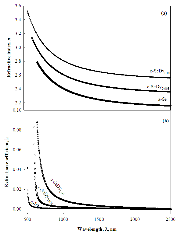 | Figure 2. Variation of refractive index (n) (a) and extinction coefficient (k) (b) with wavelength (λ) for the studied a-Se, c-SeDy0.008 and c-SeDy0.01 thin films |
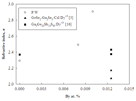 | Figure 3. Variation of refractive index as a function of the doped Dy rare earth ions in at. % for the present work [P. W.] with those published in the literature such as GeSe2-Ga2Se3-CsI [3] and Ga5Ge20Sb10S65 [16] |
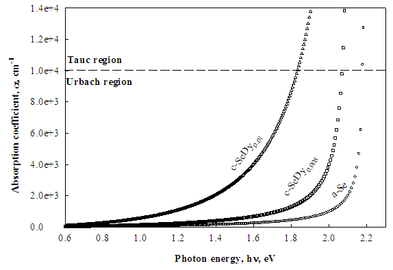 | Figure 4. The calculated absorption coefficient (α) as function of photon energy (hν) for the studied films. The dashed horizontal line differentiates between the Tauc and Urbach regions |
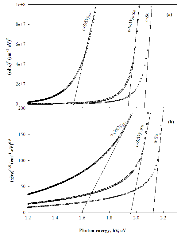
 | (1) |
 | Figure 5. Tauc’s plots for determining the optical energy gap of direct (a) and indirect (b) transitions for films investigated |
 | (2) |
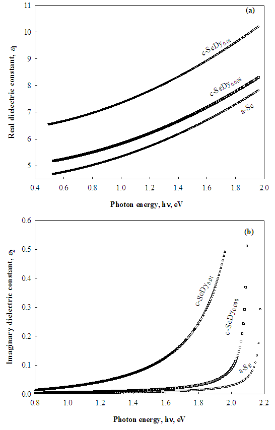 | Figure 6. Real (a) and imaginary (b) parts of the dielectric constant versus photon energy for the films investigated |
 | (3) |
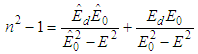
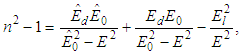
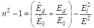
 of all the valence electrons involved in the optical transitions, ε∞ the high frequency dielectric constant, e electronic charge, c speed of light, εo free space constant, N/m* is the ratio of free carriers density to the free carrier effective mass and τ relaxation time. According to equation (3), plot of ε1 versus λ2 and extrapolating the linear part of the plot in the high wavelength region to zero wavelength gives the value of ε∞ and the slope of this line are used to calculate values of (N/m*) for the investigated films. The calculated ε∞, (N/m*) and ωp are given in Table 1, as a function of studied film compositions. The value of N/m* reflects an increase in the free carrier density with the increase of Dy-content which is argued to the metal character of Dysprosium rare earth.According to the single-effective oscillator model suggested by Wemple and DiDomenico [24], the refractive index could be described by the following relation:
 | (4) |
 | (5) |
 | (6) |
 | (7) |
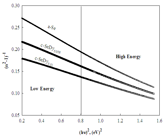 | Figure 7. Plots of (n2-1)-1 versus (hν)2 for the investigated samples |
|
 | (8) |
 | (9) |
 | (10) |
 | (11) |
 | (12) |
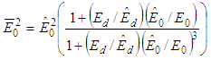
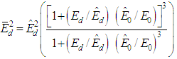
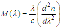
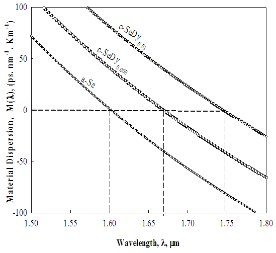 | Figure 8. Variation of the material dispersion versus wavelength for the studied films |
3.2. Non-Linear Optical Dispersion
- The microscopic nonlinear properties of the chalcogenide semiconductors have investigated through the determination of second-order refraction index, n2 and nonlinear absorption coefficient, β where n2 and β are expressed as
 | (13) |
 | (14) |
 | (15) |
 | (16) |
 | (17) |
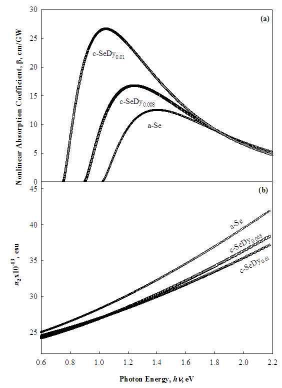 | Figure 9. Dependence of nonlinear absorption coefficient, β (a) and second order refractive index, n2 (b) on the incident photon energy, hν for the studied films |
|
4. Conclusions
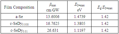
- The study of the role played by dysprosium ions as a dopant in the structural network of a-Se on optical dispersion leads to draw the main following concluding remarks: • Doping of a-Se with Dy rare earth ions assist the crystalline phase to grow on the expense of amorphous phase.• The optical band gap (Eg) decreases with increase of the Dy content which is argued to the difference in electronegativity between Se and Dy and change of part of amorphous phase to crystalline one.• The variance between the values of the optical energy gaps of the studied samples and previously published data for other chalcogenide compositions doped also with Dy are attributed to the sensitivity of chalcogenides to its thermal history and preparation conditions.• The single oscillator energy, E0, showed a decrease accompanied by an increase in the values of Ed. This trend of E0 and Ed shifted the material dispersion M(λ) towards longer wavelengths from 1.6 to 1.74 μm against the increase in the Dy-content. This shift means that the material dispersion of chalcogenide fiber could be tuned by controlling the doping ratio of Dy.• A ratio between the maximum nonlinear absorption coefficients of TPA to the optical bandgap energy equals to 1.4 is observed for different chalcogenide semiconductors.
References
| [1] | C. Liu, and J. Heo, “Generation of white light from oxy-fluoride nano-glass doped with Ho3+, Tm3+ and Yb3+,” Mater. Lett., vol. 61, pp. 3751-3754, Jul. 2007. |
| [2] | Q. Su, H. Liang, C. Li, H. He, Y. Lu, J. Li, and Y. Tao, “Luminescent materials and spectroscopic properties of Dy3+ ion,” J. Lumin., vol. 122, pp. 927-930, Jan. 2007. |
| [3] | G. Tang, Z. Yang, L. Luo, and W. Chen, “Dy 3+-doped chalcohalide glass for 1.3-μm optical fiber amplifiers,” J. Mater. Res., vol. 23, pp. 954-961, Apr. 2008. |
| [4] | N. F. Mott, and E. A. Davis, “Electronic processes in non-crystalline materials,” Oxford University Press, Oxford, Fab. 2012. |
| [5] | S. R. Elliott, “Physics of amorphous materials,” Longman Group, Longman House, Burnt Mill, Harlow, Essex CM 20 2 JE, England, 1983. |
| [6] | A. Zakery, and S. R. Elliott, “Optical nonlinearities in chalcogenide glasses and their applications,” Vol. 135, Berlin, Springer, Jan. 2007. |
| [7] | B. J. Park, H. S. Seo, J. T. Ahn, Y. G. Choi, J. HEO, and W. J. Chung, “Dy3+ doped Ge-Ga-Sb-Se glasses and optical fibers for the mid-IR gain media,” J. Ceram. Soc. Japan, vol. 116, pp. 1087-1091, 2008. |
| [8] | J. Heo, “Rare-earth doped chalcogenide glasses for fiber-optic amplifiers,” J. Non-Cryst. Solids, vol. 326, pp. 410-415, Oct. 2003. |
| [9] | Y. Shen, Y. M. Li, Q. G. Hu, W. Q. Luo, and Z. M. Wang, “Dielectric properties of B–site charge balanced Dy–doped SrTiO3 ceramics for energy storage,” J. Electroceram., vol. 34, pp. 236-240, Jun. 2015. |
| [10] | F. A. Abdel-Wahab, and H. A. Maksoud, “Electrical conduction and dielectric relaxation in selenium films doped with dysprosium rare earth,” Am. J. Cond. Matter. Phys., vol. 7, pp. 41-49, 2017. |
| [11] | V. Pamukchieva, and A. Szekeres, “Optical properties of GexSb20-xTe80 thin films and their changes by light illumination,” Opt. Mater., vol. 30, pp. 1088-1092, Mar. 2008. |
| [12] | S. Boycheva, A. K. Sytchkova, J. Bulir, C. Popov, W. Kulisch, and A. Piegari, “Optical constants of As2Se3–Ag4SSe–SnTe amorphous thin films,” J. Non-Cryst. Solids, vol. 353, pp. 1618-1623, Jun. 2007. |
| [13] | R. Swanepoel, “Determination of surface roughness and optical constants of inhomogeneous amorphous silicon films,” J. Phys. E: Sci. Instrum., vol. 17, pp. 896-903, Oct. 1984. |
| [14] | R. Swanepoel, “Determination of the thickness and optical constants of amorphous silicon,” J. Phys. E: Sci. Instrum., vol. 16, pp. 1214-1222, Dec. 1983. |
| [15] | M. Fox, “Optical Properties of Solids,” Oxford University Press, New York, 2010. |
| [16] | V. Nazabal, P. Němec, J. Jedelský, C. Duverger, J. Le Person, J. L. Adam, and M. Frumar, “Dysprosium doped amorphous chalcogenide films prepared by pulsed laser deposition,” Opt. Mater., vol. 29, pp. 273-278, Nov. 2006. |
| [17] | J. Tauc, R. Grigorovici, and A. Vancu, “Optical properties and electronic structure of amorphous germanium,” Phys. Status Solidi (b), vol. 15, pp. 627-637, 1966. |
| [18] | J. Tauc, “Optical properties of amorphous semiconductors. In amorphous and liquid semiconductors,” Springer, Boston, MA, pp. 159-220, 1974. |
| [19] | K. Sharma, M. LALb, and N. Goyal, “Optical properties of amorphous Se80-xTe20Bix thin films,” J. Optoelec. Biomed. Mater., vol. 6, pp. 27-34, Apr. 2014. |
| [20] | F. Urbach, “The long-wavelength edge of photographic sensitivity and of the electronic absorption of solids,” Phys. Rev., vol. 92, pp. 1324-1325, Dec. 1953. |
| [21] | D. Redfield, “Energy-band tails and the optical absorption edge; the case of a-Si: H,” Solid State Commun., vol. 44, pp.1347-1349, Dec. 1982. |
| [22] | M. L. Theye, A. Gheorghiu, K. Driss-Khodja, and C. Boccara, “Absorption edge in amorphous Ge and GaAs: comparative study of the role of disorder and defects,” J. Non-Cryst. Solids, vol. 77, pp. 1293-1296, Dec. 1985. |
| [23] | T. S. Moss, C. J. Burrell and B. Ellis, “Semiconductor opto-electronics,” Butterworth & Co. Ltd, New York, Dec. 1973. |
| [24] | S. H. Wemple, and M. DiDomenico Jr., “Behavior of the electronic dielectric constant in covalent and ionic materials,” Phys. Rev. B, vol. 3, pp.1338-1351, Feb. 1971. |
| [25] | S. H. Wemple, “Material dispersion in optical fibers,” Appl. Opt., vol. 18, pp. 31-35, Jan. 1979. |
| [26] | H. Poignant, “Dispersive and scattering properties of a ZrF4 based glass,” Electron. Lett., vol. 17, pp. 973-974, Dec. 1981. |
| [27] | K. Nassau, and S. H. Wemple, “Material dispersion slope in optical-fibre waveguides,” Electron. Lett., vol. 18, pp. 450-451, May 1982. |
| [28] | R.W. Boyd, “Nonlinear optics, “Academic press, USA, Jan. 2003. |
| [29] | M. Klimczak, B. Siwicki, P. Skibiński, D. Pysz, R. Stępień, A. Heidt, C. Radzewicz, and R. Buczyński, “Coherent supercontinuum generation up to 2.3 µm in all-solid soft-glass photonic crystal fibers with flat all-normal dispersion,” Opt. Express, vol. 22, pp. 18824-18832, Jul. 2014. |
| [30] | L. Liu, T. Cheng, K. Nagasaka, H. Tong, G. Qin, T. Suzuki, and Y. Ohishi, “Coherent mid-infrared supercontinuum generation in all-solid chalcogenide microstructured fibers with all-normal dispersion,” Opt. Lett., vol. 41, pp. 392-395, Jan. 2016. |
| [31] | N.L. Boling, A. Glass, and A. Owyoung, “Empirical relationships for predicting nonlinear refractive index changes in optical solids,” IEEE J. Quantum. Electron., vol. 14, pp. 601-608, Aug. 1987. |
| [32] | F. A. Wahab, F. El-Diasty, and M. Abdel-Baki, “Dispersion dependence of second-order refractive index and complex third-order optical susceptibility in oxide glasses,” Phys. Lett. A, vol. 373, pp. 3855-3860, Oct. 2009. |
| [33] | C. Quémard, F. Smektala, V. Couderc, A. Barthelemy, and J. Lucas, “Chalcogenide glasses with high nonlinear optical properties for telecommunications,” J. Phys. Chem. Solids, vol. 62, pp. 1435-1440, Aug. 2001. |
| [34] | F. Smektala, C. Quemard, L. Leneindre, J. Lucas, A. Barthélémy, and C. De Angelis, “Chalcogenide glasses with large non-linear refractive indices,” J. Non-Cryst. Solids, vol. 239, pp.139-142, Oct. 1998. |
| [35] | R. Rangel-Rojo, K. Kimura, H. Matsuda, M. A. Mendez-Rojas, and W. H. Watson, “Dispersion of the third-order nonlinearity of a metallo-organic compound,” Opt. Commun., vol. 228, pp.181-186, Dec. 2003. |
| [36] | L. Petit, N. Carlie, R. Villeneuve, J. Massera, M. Couzi, A. Humeau, G. Boudebs, and K. Richardson, “Effect of the substitution of S for Se on the structure and non-linear optical properties of the glasses in the system Ge0.18Ga0.05Sb0.07S0.70-xSex,” J. Non-Cryst. Solids, vol. 352, pp. 5413-5420, Dec. 2006. |
| [37] | A. Zakery, and S. R. Elliott, “Optical properties and applications of chalcogenide glasses: a review,” J. Non-Cryst. Solids, vol. 330, pp. 1-12, Nov. 2003. |
| [38] | K. Petkov, and P. J. S. Ewen, “Photoinduced changes in the linear and non-linear optical properties of chalcogenide glasses,” J. Non-Cryst. Solids, vol. 249, 150-159, Jul. 1999. |
| [39] | J. Requejo-Isidro, A. K. Mairaj, V. Pruneri, D. W. Hewak, M. C. Netti, and J. J. Baumberg, “Self refractive non-linearities in chalcogenide based glasses,” J. Non-Cryst. Solids, vol. 317, pp. 241-246, Mar. 2003. |