Banafshe Yaghtin , Rahim Ghayour , Mohammad Hossein sheikhi
Department of Electronic and Communication Engineering, Shiraz University, Shiraz, Iran
Correspondence to: Banafshe Yaghtin , Department of Electronic and Communication Engineering, Shiraz University, Shiraz, Iran.
| Email: |  |
Copyright © 2017 Scientific & Academic Publishing. All Rights Reserved.
This work is licensed under the Creative Commons Attribution International License (CC BY).
http://creativecommons.org/licenses/by/4.0/

Abstract
The objective of this research is design and simulation of a single quantum well laser (SQW) to observe the effects of quantum well number increment and temperature variation on the performance of this laser. This laser is structured of three different compounds GaN, InGaN and AlGaN with different mole fractions. It has a cavity length of 300 um and a width of 30 um. This laser has designed to be a high power laser at room temperature and continues wave condition. The optimized number of quantum wells to obtain the highest optical power is 2. The double quantum well (DQW) structure of this an ultraviolet at room temperature with a wavelength of 326 nm and maximum optical power of 16W.
Keywords:
Gallium nitride semiconductor lasers, MQW lasers, Band gap energy traps, Carrier mobility
Cite this paper: Banafshe Yaghtin , Rahim Ghayour , Mohammad Hossein sheikhi , Reversed Effects of Quantum Well Numbers and Temperature on Optical Power and Wavelength of a Designed Ultraviolet Semiconductor Laser Based on GaN/InGaN, International Journal of Optoelectronic Engineering, Vol. 7 No. 1, 2017, pp. 13-18. doi: 10.5923/j.ijoe.20170701.02.
1. Introduction
In recent years, Gallium-nitride optoelectronic devices have been the most attractive productions because of their performance near UV, blue and green wavelengths. In addition, GaN and related alloys are also being used in high power, high frequency, high temperature bipolar and field effect transistors and multi-junction solar cells [1]. There is a strong interest in development of multi quantum well semiconductor lasers based on GaN/InGaN in some applications like high density optical power and energy efficient lighting [2]. Usage of quantum well lasers to increase the output power in semiconductor devices has been started science many years ago. However rise in quantum well numbers is one of the well known approaches to increase the optical power in optical semiconductor devices, sometimes increase in number of quantum wells more than a limited number will contribute to some reversed effects, such as rise in threshold current and reduction in optical power. To show this fact, we have designed and simulated a single quantum well semiconductor laser (SQW) based on GaN and have grown the number of QWs from one to six to describe physical effects of this variation on multi quantum well structures (MQW) at room temperature. The laser performance resembles a high power UV laser diode with a wavelength of 362 nm. Ultraviolet lasers have applications in industry (laser engraving), chemistry (MALDI), free air secure communications [3], medicine (dermatology, and keratectomy), dental (curing of polymers), computing (optical storage) and manufacture of integrated circuits [4]. Finally, we have studied optical power and wavelength variation of DQW structure for temperatures less and more than room temperature.
2. Experiment
2.1. Design of Laser Structure
The designed SQW laser in this research has an active region, including one In0.08Ga0.92N quantum well and two GaN barriers with thicknesses of 3 nm and 5 nm respectively. As it can be seen in Figure 1, this active region has surrounded by two GaN waveguide layers and two Al0.07Ga0.93N cladding layers with thicknesses of 0.1 um and 0.4 um. There are GaN waveguide layers and a GaN layer contacting to anode layer with thickness of 0.1 um. All top layers are p-type and doped to 5 × 1018 cm-1 of acceptors. The substrate with thickness of 0.55 um and other bottom layers are n-type and doped to 9 × 1017 cm-1 of donors. To prevent current leakage we have gained an Al0.15Ga085N block layer with a thickness of 0.02um in this structure. We have simulated this p-n heterostructure as SQW and MQW diode lasers with different number of quantum wells at 300 K.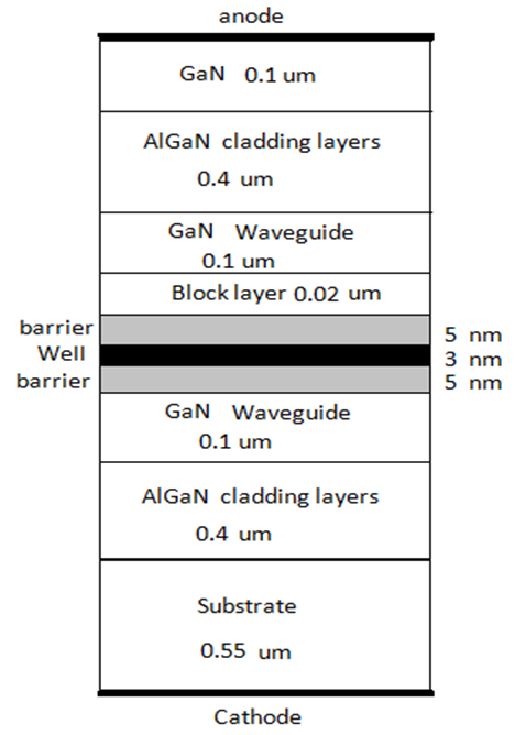 | Figure 1. Sample structure of the SQW laser |
2.2. Simulation Results and Theoretical Analysis
As you know one of the most important parameters which has defined for a quantum well is density of states in the well. For a SQW laser the density of states is as: 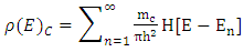 | (1) |
Where  and
and  are the Heaviside function, the effective mass of electrons, Planck’s constant and quantized energy level of electrons in the nth subband of quantum wells, respectively [4]. En is equal to:
 | (2) |
Where  is thickness of quantum well [4].If we use a MQW structure instead of the SQW, the density of states will modified. When barrier layers between wells are thick enough, each well would be independent and in this situation, the density of states is just N times density of states in an SQW [4].
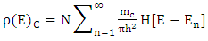 | (3) |
Where, N is number of wells.Increase in quantum density of states leads to increase in photon absorption by quantum wells so that the optical power of MQW lasers should be N times more than optical power in SQW. Also, we expect to need less threshold current density by increasing the number of QWs. As Figure 2 illustrates, the simulated SQW structure of this laser has threshold current and optical power of 60 mA and 9W respectively and in term of DQW structure, the output optical power of laser has increased dramatically to a high power of 16w. According to equation (3), this amount is approximately twice the optical power of SQW structure. In the next step, we increased QWs numbers to three to achieve a higher optical power. However according to equation (3), we expect optical power of 3QW laser become 3 order greater than optical power of SQW laser, conversely it has dropped down to 10W and its threshold current has risen to 60 mA as is shown in Figure 2. | Figure 2. Illustration of Optical power-Current curve of SQW and MQW structures of laser |
Thereafter, we increased the number of QWs to 4, 5 and 6 numbers. As it has illustrated in Figure 2, output optical power of these lasers has reduced gradually to 9W, 6W and 3W and threshold current has upward trade to reach 80 mA. These observed results couldn’t be compatible with which we had predicted with attention to equation (3). To find and describe the reasons of these unexpected and reserved results we have a discussion in the next stage. To study the effective factors which contribute to observed results there are several major explanation. Firstly, as we increase the number of wells, the density of states and consequently the photon absorption in active region will rise. This rise stimulates more number of electrons to conductive band, so that more free holes and electrons will created in active region and as the result, probability of direct transitions to valance band which make radiative recombination and photon emission in active region increase considerably. However, Figure 3 is demonstration of the active region in 6QW structure. As you can see in this figure, there is a high concentration of electrons between conductive and valance bands. This high concentration of electrons leads to reduction of mobility and velocity of electrons. In addition, electrons will hit to each other and loss a percentage of their energy because of these hits. In such situation, electrons don’t have enough energy to get to valance band and recombine with holes of valance band. Thus, by reducing hole and electron recombination which contributes to photon emission in active region of 6QW laser, the optical power of this laser has declined to 3W as is observable in Figure 2.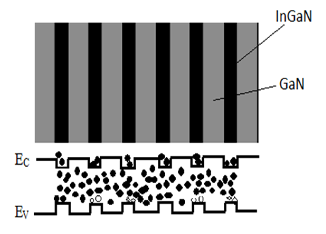 | Figure 3. A schematic of active region for 6QW laser structure |
The second critical factor which has an important impression on optical power of QW lasers could be the thickness of barriers. As it has demonstrated in Figure 4, when the barriers are thick enough, quantum wells are separated with degenerated energy levels. When the thickness of barriers become very narrow, tunneling coupling will happen and electrons of each well tunnel across the barriers so that there is a probability of electron attendance in the other energy levels.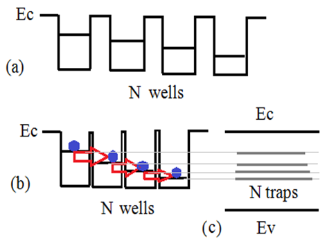 | Figure 4. Formation of new band gap energy, (a) N separated quantum well laser with their energy levels, (b) tunneling coupling and splitting of a single energy level to N levels, (c) new band gap energy with N traps |
As the consequence, each energy level splits into series of N levels, where N is the number of wells. As the matter of fact, tunneling among the wells breaks this degeneracy of energy levels and results in creation of new band gap energy which consisted of N energy levels. Figure 4 indicates this fact clearly [5]. In this research, the thickness of barriers for designed devices is 5 nm which is very thin and leads to tunneling coupling. Therefore, by increasing QW numbers to a larger number, more number of energy levels will create in band gap energy. As the result, when electrons of valance band stimulated to conduction band, the N energy levels act as traps or defect centers for electrons in band gap energy. The presence of these traps in semiconductor may significantly influence the electrical characteristics of the device. These trap centers could change the density of space charge in semiconductor bulk and influence the recombination statistics. Traps cause indirect and nonradiative recombination in structure. Thus, increase in quantum well numbers leads to create more traps in band gap energy, more indirect recombination and more thermal energy production instead of photon emission. Figure 5 displays difference of electron transition and recombination in band gap energy with and without traps.Also, by increasing trap numbers in active region the separation of excitions gets more sever and the overlap of hole and electron wave functions decreases gradually in further wells. As the result, the most recombination of holes and electrons occurs in first and second well before the number of traps increased.In addition, the lifetime of holes is expressed as [6]: | (4) |
Where c is the capture probability coefficient and depends on intrinsic characteristics of material and  is the number of traps in the band gap energy [6]. Besides, there are relationships between the life time of holes
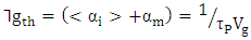
  threshold modal gain
  internal optical loss
 and mirror loss
  in diode lasers as [7]:
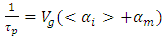 | (5) |
 | (6) |
Where  is the group Velocity.
 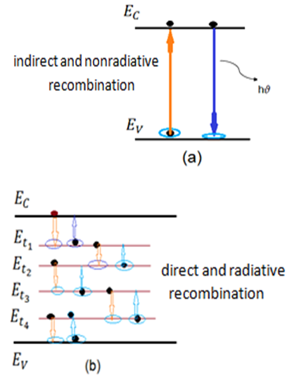 | Figure 5. Schematic of electron transition in band gap energy a) without traps b) with traps |
According to equation (4), the hole lifetime is strongly depends on trap numbers and increasing in number of traps, results in reduction of hole lifetime. In the other hand, with a great attention to equation (5) and (6) we can reveal, reduction in life time of holes contributes to rise in internal optical loss and threshold modal gain of diode laser. It could one of the another major reasons of reduction the optical power by increasing the QW numbers. The optical power of diode lasers can be written as equation (7) and indicates this fact [7].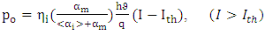 | (7) |
Where h is the plank constant,  is injection efficiency and
  is the frequency of emitted photon. Moreover, the threshold current of laser diodes can displayed as [7]:
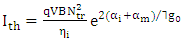 | (8) |
Where B is bimolecular recombination coefficient, g0 is gain coefficient and  is the transparency carrier density [7]. This equation expresses, increasing the internal optical loss leads to increase in threshold current of diode laser. Besides, as it is observable in Figure 2, there is a kink near the threshold currents in P-I characteristic of lasers. The main reason of these kinks refers to the starting of stimulated emission which leads to the first recombination of stimulated electrons and holes begins and lasing takes place in structure. Figure 6, represents this reason clearly [7].
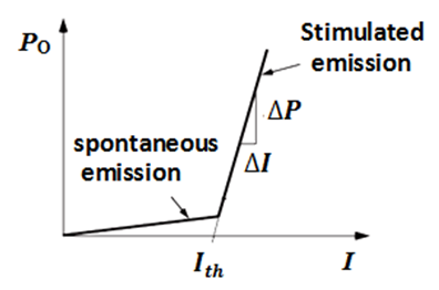 | Figure 6. Illustration of output power versus current for a diode laser, below threshold only spontaneous emission is important; above threshold the stimulated emission power increases while the spontaneous emission is clamped at its threshold value [7] |
The differential quantum efficiency would be found by taking divergent of  and could be expressed as [7]:
 | (9) |
The slop of lines which is illustrated in Figure 2 shows the differential quantum efficiency of designed lasers which has a maximum value in DQW structure and it has diminished gradually by increasing the QW numbers.Finally, the trade of threshold current and optical power characteristics of this structure based on QW number can be shown as Figure 7.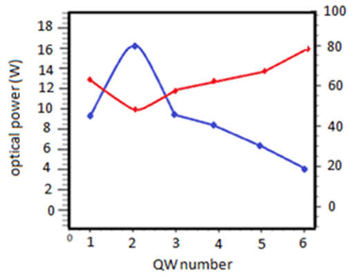 | Figure 7. The optical power and threshold current curves of laser based on quantum well numbers |
2.3. Temperature Effects on DQW Designed Structure
Firstly, to study the effects of temperature on this designed diode laser, it is essential to know band gap energy of semiconductors is strongly depends on temperature and mole fraction. In materials including GaN, InN and InxGa1-xN the band gap energy is expressed by [8]: | (10) |
 | (11) |
 | (12) |
Besides the optical wavelength of diode laser is deeply attached to band gap energy [9]: | (13) |
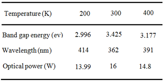
As the result of recent equations, properties of  with mole fraction of 0.08 and at three different temperatures would be found as table 1.
Table 1. Some parameters of DQW InGaN laser with mole fraction of 0.08 at different temperatures
 |
| |
|
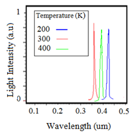 | Figure 8. Illustration of output optical wavelength for DQW laser at different temperatures |
As you observe in table 1 and Figure 8, the DQW structure has wavelengths of 391nm and 362 nm at 200K and 300K respectively so that this structure regarded as an ultraviolet laser at these temperatures. In addition, at temperatures more and lower than 300 K this laser has a lower optical power and light intensity in comparison to 300 k. The major reason is deeply attached to mobility of carriers at these temperatures.The electron mobility is given by:  | (14) |
Where  and
and  are lattice mobility and scattering mobility respectively and
  is electron mobility [6].As these MQW designed lasers have a p-n junction so that active region of these lasers is a depletion region. Thus, according to Figure 9, there is the least doping concentration of impurity in active region and under forward bias this doping concentration is located at besides of depletion layer. Consequently, based on equation 14, the electron mobility in active region s only depended on lattice mobility. In the other hand, the low temperatures reduce lattice scattering and thermal velocity of electrons, so that lattice mobility and electron mobility will reduce. Note that the mobility of electrons is higher than that of holes. When temperature increases, thermal velocity of carriers and lattice scattering grow too and the mobility of electrons reaches to its peak at 300k.
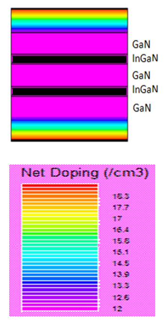 | Figure 9. Simulation of doped impurity in active region for DQW laser |
At higher temperatures, carrier velocity and lattice scattering increase more and more. Therefore carriers hit more to each other and to lattice atoms. It staves off their fast moving so that their mobility falls gradually. As we mentioned before, reduction in mobility of electrons and holes leads to rise in their lifetime and optical recombination probability. In fact, at room temperature, carriers have their best mobility and laser has its extreme light intensity and optical power [6, 10]. Based on these described reasons and results, the mobility variation of electrons and holes with temperature for In0.08Ga0.92N will be demonstrated as Figure 10. 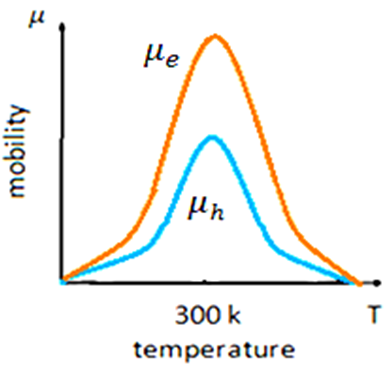 | Figure 10. Illustration of hole and electron mobility variation with temperature for InGaN with mole fraction of 0.08 |
The reversed effects of increase in QW numbers are not correct about all kinds of semiconductor lasers. In some specific types such as cascade quantum well semiconductor lasers with no p-n junction, increase in quantum well numbers with different thicknesses and at several periods leads to increase in optical power of laser [11]. However, these sorts of lasers have a barrier thickness of nanometer and tunneling coupling occurs in them, subband energy levels of quantum wells don’t act as traps. In fact, photon emission could be obtained by electron transition among the energy levels of quantum wells in conduction or valance band [12, 13].
3. Conclusions
Based on this research, we find out increase in quantum well numbers more than a limited number in semiconductor lasers with p-n junction (laser diodes) leads to some undesirable results such as optical power reduction and rise in threshold current. The main reasons of this fact depends on three key factors: I) Increase in quantum well number results in high photon absorption and high concentration of free carries in active region. It leads to reduction in carrier mobility and the chance of optical recombination. II) Thin thickness of barriers results in tunneling couplings of N quantum wells and creation of N traps in band gap energy. It causes indirect recombination instead of optical recombination. III) As QW numbers increased, the overlap of exited electron and holes reduces. In addition, we reveal quantum well lasers based on GaN and InGaN with mole fraction of 0.08 has the best performance at room temperature when their structure is DQW and diode lasers the mobility of electrons and holes of active region is only depends on lattice mobility.
ACKNOWLEDGEMENTS
I would like to acknowledge Professor Rahim Ghayour and Professor Mohammad Hossein Sheikhi from communication and electronic engineering department of Shiraz University, because of all their valuable and helpful subjects they have taught me during my Master's education and my thesis.
References
| [1] | S. Nakamura, GaN and Related materials II, Gordon and Bre each, pp. 1–45, (1999). |
| [2] | S. Shur, M.A. Khan, GaN and Related materials, II, Gordon and Breach, pp. 47–92, (1999). |
| [3] | C. Lee, C. Shen, C. Cozzon, Gigabite-pre-second white light-based visible light communication using near-ultraviolet laser diode and red, green and blue emitting phosphors, Opt.Express,17480, Vol.25, (2017). |
| [4] | Vladimir Panov, Tsvetelina Borisova, Application of ultraviolet light (UV), MedInform, 201522.194, (2015). |
| [5] | Daniel L. Becerra et al, Chemically assisted ion beam etching of laser diode facets on nonpolar and semipolar orientation of GaN Appl.Phys.Express, 092104, Vol9, (2016). |
| [6] | Edward S. Yang, Microelectronic devices, McGraw Hill, pp. 29- 45, (1988). |
| [7] | L. A. Coldren and S.W. Corzine, Diode Lasers and photonic Integrated Circuits, John Wiley & Sons, Inc pp.1-263 (1995). |
| [8] | C. Shen, G.O. Mueller, S. Watanabe, N.F. Gardner, Auger recombination InGaN measured by photo luminescence, Journal of Appl.phys.Lett., 141101–141103, (2007). |
| [9] | Harry J. R. Dutton, Understanding optical communication, International Technical Support Organization, pp.74-84, (1998). |
| [10] | Daniel Becerra, Daniel A Cohen, Robert M Farrell, High efficiency semipolar III-nitride lasers for solid state lighting, International Semiconductor Laser Conference, IEEE, (2016). |
| [11] | Wanga, C.A., Goyal, A.K., S. Menzel, Calawa, D. Rconnors, M.K., Sanchez, A., Turner, G. Capasso, F., Highpower,  quantum cascade lasers grown by OMVPE, Journal of Crystal Growth 370, 212-216, (2013). quantum cascade lasers grown by OMVPE, Journal of Crystal Growth 370, 212-216, (2013). |
| [12] | Katz Simeon, Augustinas Vizbaras, Ralf Meyer and Murkus Amann, Injectorless quantum cascade lasers, Journal of Appl. Phys109, 081101, (2011). |
| [13] | Banafshe Yaghtin, Rahim ghayour, Mohammad Hossein Sheykhi, International Journal of multidisciplinary science and engineering, Design and Simulation of two continues wave AlGaAs/GaAs Semiconductor Cascade Quantum Well Lasers at room temperature, Vol8, NO 4, (2017). |

 Abstract
 Reference
 Full-Text PDF
 Full-text HTML