-
Paper Information
- Paper Submission
-
Journal Information
- About This Journal
- Editorial Board
- Current Issue
- Archive
- Author Guidelines
- Contact Us
International Journal of Optoelectronic Engineering
p-ISSN: 2167-7301 e-ISSN: 2167-731X
2014; 4(1): 11-15
doi:10.5923/j.ijoe.20140401.03
Optical and Electrical Properties of CdO: Sn Thin Films for Solar Cell Applications
 Abstract
 Reference
 Full-Text PDF
 Full-text HTML
N. E. Makori, I. A. Amatalo, P. M. Karimi, W. K. Njoroge
Department of Physics, Kenyatta University, Nairobi, Kenya
Correspondence to: N. E. Makori, Department of Physics, Kenyatta University, Nairobi, Kenya.
| Email: |  |
Copyright © 2014 Scientific & Academic Publishing. All Rights Reserved.
Tin doped Cadmium Oxide (CdO:Sn) thin films were successfully deposited by thermal evaporation in the Edward’s Auto 306 Magnetron Sputtering System. Their optical and electrical properties were studied using Solid Spec-3700 DUV Spectrophotometer and Four Point Probe respectively. The optical properties of CdO:Sn thin films showed high transparency in the visible region of the electromagnetic spectrum which varied with Sn doping, this makes CdO:Sn an excellent candidate for optoelectronic applications such as a window layer. Undoped Cadmium Oxide (CdO) thin films were also prepared for comparison with tin doped Cadmium Oxide thin films. Doped and undoped Cadmium Oxide had a transmittance of 70-85% and 50-89% respectively. Band gap energy for undoped CdO was 2.43eV while that of tin doped CdO ranged between 3.19-3.29eV for tin doping of 1-7%. Resistivity of undoped and Tin doped Cadmium Oxide ranged between 16-93Ωcm.
Keywords: Thermal evaporation, Tin doping, Optical properties, Electrical properties
Cite this paper: N. E. Makori, I. A. Amatalo, P. M. Karimi, W. K. Njoroge, Optical and Electrical Properties of CdO: Sn Thin Films for Solar Cell Applications, International Journal of Optoelectronic Engineering, Vol. 4 No. 1, 2014, pp. 11-15. doi: 10.5923/j.ijoe.20140401.03.
Article Outline
1. Introduction
- Energy consumption has increased steadily with civilization. Energy crisis due to a decline in fossil fuel stocks and increasing carbon dioxide emissions that are causing global warming has enhanced interest in the development of clean renewable sources of energy. To sustain human development, more electrical energy consumption is expected in future [1]. Solar cells hold great hopes for use as an environmental friendly and economically viable renewable source of energy.Cadmium Oxide (CdO) is an important semiconductor material for the development of various technologies of solid-state devices. The semiconducting thin films of CdO are transparent in visible and NIR spectral regions [2]. Cadmium Oxide is an n-type semiconductor with Sodium Chloride structure. It has a direct optical band gap of 2.3 eV. It has a high electrical conductivity that is attributed to moderate electron mobility and higher carrier concentration due to the contribution from shallow donors resulting from inherent non-stoichiometry. Non-stoichiometric undoped CdO thin films usually exhibit low resistivity due to native defects of Oxygen vacancies and Cadmium interstitials [3]. Optically, it is a transparent material over energies of 540 nm in the solar spectrum. Cadmium Oxide thin films find wide applications in the field of optoelectronic devices such as solar cells, transparent electrodes, photodiodes among others. For example CdO transparent conducting oxide prepared by [4] with a band gap of 2.3 eV and an electron affinity of 4.5eV were used for fabricating CdO/CdTe heterostructure solar cells with efficiencies of 9.1% by DC magnetron sputtering.The conduction of pure CdO is attributed to its native defects of Oxygen vacancies and Cadmium interstitials. Therefore, the conductivity of CdO thin films can be controlled by those native defects through the procedure of thin film preparation including doping with metallic ions. Cadmium Oxide can be doped with various dopants for example fluorine and tin. Fluorine doping of CdO, shifts the optical band gap along with the increase in transparency of CdO films. Tin-doped Cadmium Oxide (CdO:Sn) deposited by [5] using atmospheric pressure metalorganic chemical vapour deposition technique, showed that the highly transparent and conductive CdO:Sn thin films are promising for photovoltaic applications. The structural, electrical and optical properties of the fabricated thin films were influenced by partial pressure of Dimethylcadmium and Tetramethyltin, substrate temperature, film thickness and annealing conditions. A sheet resistance of (14-17) Ω/square units were obtained for as-deposited CdO:Sn thin films with a thickness of (120-150) nm. The transmission of the films in the visible range was high (80-95) % and shifted towards the blue region due to the Moss-Burstein (M-B) effect. The films exhibited direct and indirect band-to-band transitions, which corresponded to optical band gaps of 3.0 and 2.5eV, respectively. The electro-optical properties of as-deposited CdO:Sn thin films were further improved by post-deposition annealing. A resistivity value of (1.4-1.6) x 10-4Ωcm was obtained after annealing in Helium and Hydrogen ambient. CZT/CdO cells were categorised in two groups [6], namely type A and B. A: SnO2/CdO/CZT structure, B: SnO2/CdS/CdO/CZT structure. In type A, evaporation of CdO led to the formation of CdO/SnO2 junctions which had Voc in the range of 100-250 mV. The current densities of devices made were in the range of 4-6 mA/cm2. Type B devices had higher current densities ~8mA/cm2. The Voc were in the range of (200-280) mV. This showed that carrier concentration varied with the proportion of Cadmium in the cell. Tin doped CdO thin films prepared by [7] using electron beam technique exhibited direct band-to-band transitions, which corresponded to optical band gaps of 3.1– 3.3 eV with a transmittance value of ~83% and a resistivity value of 4.4×10⁻⁴ Ωcm were achieved for (CdO)0.88(SnO2)0.12 film annealed at 350℃ for 15 minutes, whereas the maximum value of transmittance ~93% and a resistivity value of 2.4×10⁻³ Ωcm were obtained at 350℃ for 30 minutes. Transparent conducting CdO:Sn films deposited by [8] Metal Organic Chemical Vapour Deposition for application in CdTe/CdS solar cells had a conversion efficiency of 14.3%. The films had a sheet resistance of 14-17Ω/square for a film of thickness of 120-125 nm. The effect of substrate temperature studied by [9] on electrical and optical properties of CdO:Sn deposited by Pulsed Laser Deposition Technique found that the films were highly transparent (78-89%) in the visible region. The resistivity increased with growth temperature and the lowest resistivity of 1.96 x 10⁻⁵ Ωcm was observed for the films grown at 150℃. These highly conducting and transparent tin-doped CdO thin films could be an excellent candidate for current and future solar cell applications.
2. Experimental Procedure
- Reactive thermal evaporation of CdO and CdO:Sn thin films was done in Edwards Auto 306 Magnetron Sputtering System. To prepare Cadmium Oxide, Cadmium was heated in glass tube until it melted. It was allowed to cool in sealed glass tube to prevent oxidation of Cadmium. Clean glass substrates were then mounted on a substrate holder of the Edwards Auto 306 Magnetron Sputtering System. About 1g of Cadmium was placed on a boat and then the chamber covered tightly and evacuated. A constant current of 3.0A was supplied to the heater to evaporate the material in presence of oxygen at a flow rate of 20 sccm and a chamber pressure of 3.8 x 10⁻⁵ mbar form CdO thin films. To prepare CdO:Sn thin films, Cadmium and Tin were mixed at predetermined ratios (Tin doping ranging from (1-7)%. Cadmium and Tin were heated in glass tubes until they melted. They were allowed to cool in sealed glass tubes to prevent oxidation of Cadmium and Tin. Clean glass substrates were then mounted on a substrate holder of the Edwards Auto 306 Magnetron Sputtering System. About 1g of Cadmium and Tin alloy were placed on a boat and then the chamber covered tightly and evacuated. The deposition conditions for the films are shown in table 1.
3. Results and Discussions
3.1. Transmittance of CdO and CdO:Sn
- Transmittance of undoped CdO was between 70-90 % for photons of wavelength between 350-800 nm while that of 1-7 % Sn doped CdO was between 62-89 % for photons of wavelength between 350-800 nm. Transmission values between 83-89% were obtained for photons of wavelength 500-628nm for 1- 4% Sn doped CdO samples. However, when Sn concentration increased beyond 5% the transmission spectra decreased, this is probably due to the disorder in the lattice which increases in the localized states near the bands. High transmittance values of Sn doped CdO thin film samples is a clear indication that CdO:Sn is appropriate for use as a window layer in photovoltaic applications. The transmittance spectra of doped and undoped CdO are shown in figure 1.
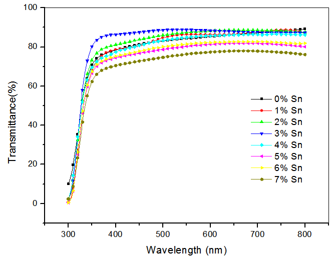 | Figure 1. Transmittance spectra of 0-7% Sn doped CdO |
3.2. Energy Band Gap of CdO and CdO:Sn
- The band gap, Eg was extracted from transmittance data simulated using SCOUT 2.4 software. Energy band gap can also be obtained from straight line plots of (Ahυ)2/n as a function of hυ: an extrapolation of the value of (Ahυ)2/n to zero, also gives Eg. If a straight line for n=1 is obtained, then there is a direct electron transition between the states of the semiconductor, whereas for n=4, the electron transition is indirect. The variation of optical band gap with tin doping is shown in figure 2.
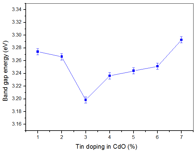 | Figure 2. Variation of band gap energy of CdO thin films with tin doping |
 | (1) |
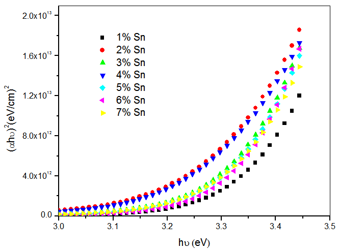 | Figure 3. Plots of (αh)2 versus photon energy hυ for CdO:Sn thin films |
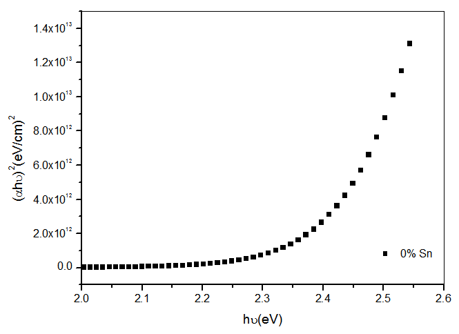 | Figure 4. Plot of (αhυ)2 versus photon energy hυ for undoped CdO thin films |
4. Electrical Resistivity of CdO and CdO:Sn
- Sheet resistance was measured using Four Point Probe. Resistivity of CdO and CdO:Sn ranged between (16 - 93) Ωcm. The variation of resistivity with tin doping is shown in table 2 and figure 5.
|
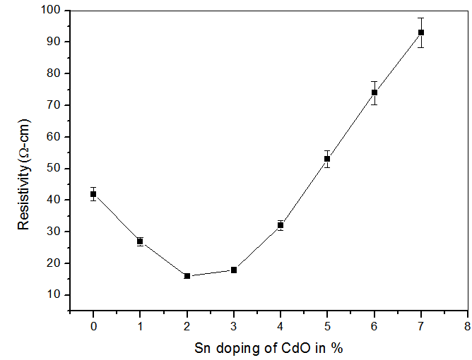 | Figure 5. Variation of electrical resistivity of CdO:Sn thin films with tin doping |
5. Conclusions
- Undoped CdO and Tin doped CdO thin films were successfully deposited on glass substrate using thermal evaporation and reactive thermal evaporation respectively under different deposition conditions. The effects of 0-7% Sn doping of CdO on optical and electrical properties of CdO respectively were investigated.The transmittance increased and the resistance dropped as the Sn doping is increased from 1-3% due to creation of impurity states in the forbidden energy gap. Further increase of the doping level results in the phase segregation and a band filling which impact the sheet resistance and transmittance respectively.Since Sn doping improved optical and electrical properties of CdO, Sn doped CdO thin films have potential applications as Transparent Conducting Oxide material in photovoltaic cells and other optoelectronic device applications.
ACKNOWLEDGEMENTS
- We thank the Chairman Physics Department Dr. Charles Migwi Kenyatta University 2006-2011 for providing the facilities for the research work. We also extend our heartfelt thanks to the laboratory technicians under the guidance of the Chief Technician Mr. Simon Njuguna particularly in their technical input in the maintenance of the Edwards magnetron Sputtering System. Our special thanks also go to Mr. Boniface Muthoka; technician Physics Department University of Nairobi-Chiromo Campus for his technical input in the use of the Solid Spec 3700 DUV Spectrophotometer.
References
| [1] | Kuo-Jui, H. (2010). Electron-reflector strategy for CdTe thin-film solar cells. PhD Thesis. Colorado State University, Department of Physics, USA. |
| [2] | Hamadi, O.A., Shakir, N.J. and Mohammed, F.H. (2010). Magnetic field and temperature dependent measurements of hall coefficient in thermal evaporated tin-doped cadmium oxide thin films. Physics journal, 37, 223–231. |
| [3] | Zhiyong, Z., Morel, D. L. and Ferekides, C. S. (2002). Electrical and optical properties of tin-doped CdO films deposited by atmospheric metalorganic chemical vapor deposition. Thin Films. 413, 203-211. |
| [4] | Subramanyama, T.K., Mohan, G.R. and Uthanna, S. (2001). Process parameter dependent property studies on CdO films prepared by DC reactive magnetron sputtering. Materials chemistry and physics, 69, 133-142. |
| [5] | Deokate, R.J, Pawar, S.M, Moholkar, A.V, Sawant, V.S, Pawar, C.A, Bhosale, C.H and Rajpure, K.Y. (2008). Spray deposition of highly transparent fluorine doped cadmium oxide thin films. Applied surface science, 254, 2187-2195. |
| [6] | Gowri, S. (2003). Characterization of cadmium zinc telluride solar cells. Msc thesis. University of South Florida, College of Engineering: Department of Electrical Engineering. USA. |
| [7] | Ali, H. M., Mohamedy, H. A., Wakkad, M. M., and Hasaneen, M. F. (2009). Optical and electrical properties of tin-doped cadmium oxide films prepared by electron beam technique. Japanese journal of applied physics, 48, 1-7. |
| [8] | Zhiyong, Z., Komin, V., Viswanathan, V., Morel, D.L., Ferekides, C.S. (2000). Application of tin-doped Cadmium oxide films in CdTe/CdS solar cells. Photovoltaic specialists conference report. |
| [9] | Gupta, R.K., Ghosh, K., Patel R., Mishra, R.S. and Kahol, P.K. (2008). Effect of oxygen partial pressure on optoelectrical properties of tin - doped CdO thin films. Journal of optoelectronics and advanced materials, 10, 2611 – 2615. |
| [10] | Rusu, R.S. and Rusu, G.I. (2004). The hall effect in CdO:Sn thin films. D. Mangeron, Romania. |
| [11] | Vigil-Galán, O., Sánchez-González, Y., Arias-Carbajal, A., Contreras-Puente, G., Tufiño-Velázquez, M and Ruiz, C.M. (2006). Influence of Sn concentration on the physical properties of CdO:Sn thin films deposited by spray pyrolysis. Solid state physics, 15, 3713–3719. |
| [12] | León-Gutiérrez, L.R., Cayente-Romero, J.J., Peza-Tapia, J.M., Barrera-Calva, E., Martínez-Flores, J.C. and Ortega-López, M. (2006). Some physical properties of Sn-doped CdO thin films prepared by chemical bath deposition. Materials letters, 60, 3866 - 3870. |
| [13] | Zheng, B.J., Lian J.S., Zhao, L. and Jiang, Q. (2011). Optical and electrical properties of Sn-doped thin films obtained by pulse laser deposition. Vacuum technology, 85, 861-865. |