-
Paper Information
- Paper Submission
-
Journal Information
- About This Journal
- Editorial Board
- Current Issue
- Archive
- Author Guidelines
- Contact Us
International Journal of Optoelectronic Engineering
p-ISSN: 2167-7301 e-ISSN: 2167-731X
2014; 4(1): 6-10
doi:10.5923/j.ijoe.20140401.02
Ultrafast and High Sensitive UV/IR Photodetector Based on a Single SnO2 Nanowire
 Abstract
 Reference
 Full-Text PDF
 Full-text HTML
Abdelrahim Ate, Zhenan Tang
School of Electronic Science and Technology, Faculty of Electronic Information and Electrical Engineering, Dalian University of Technology, Dalian 116024, P.R. China
Correspondence to: Zhenan Tang, School of Electronic Science and Technology, Faculty of Electronic Information and Electrical Engineering, Dalian University of Technology, Dalian 116024, P.R. China.
| Email: |  |
Copyright © 2014 Scientific & Academic Publishing. All Rights Reserved.
Tin oxide, SnO2 has potential applications in many research areas. Using a chemical vapor deposition CVD method, high-quality single crystalline SnO2 nanowire (NW) was synthesized on a large scale. Individual SnO2 nanowire based ultraviolet photodetector was fabricated by simply transferring individual nanowire to Pt interdigital electrodes. The photodetector exhibited excellent photoconductive performance in terms of high sensitivity to the ultraviolet 375 nm and infrared 750 nm UV illuminations, fast response and recovery time. It also has perfect stability and reliability, revealing n-type semiconducting behaviour of the tin oxide ultraviolet and infrared photodetecors as an excellent material not only for fabricating highly sensitive photodetecors but also valuable additives that provide new functionality in photodetecors, which will enable the development of high-performance photodetecors.
Keywords: SnO2 nanowires, Chemical vapor deposition, UV/IR photodetector
Cite this paper: Abdelrahim Ate, Zhenan Tang, Ultrafast and High Sensitive UV/IR Photodetector Based on a Single SnO2 Nanowire, International Journal of Optoelectronic Engineering, Vol. 4 No. 1, 2014, pp. 6-10. doi: 10.5923/j.ijoe.20140401.02.
Article Outline
1. Introduction
- One dimensional (1-D) nanostructures had a great potential for applications in the fields of the optoelectronic and sensor device. Tin oxide (SnO2) is an n-type semiconductor with a wide-band gap (Eg = 3.62 eV, at 300 K). Furthermore, because of the wide-band gap, very large surface to volume ratios, low cost, high responsive, strong radiation hardness and high chemical stability. Photodetectors can be used for a variety of applications in the military, scientific, civil applications, security, medicine, industrial, automotive areas and communications. Common applications using UV/IR detectors include rail safety, gas leak detection, flame detection, alcohol level testing for DUI’s, anesthesiology testing, petroleum exploration, space operations, temperature sensing, water and steel analysis [1] [2] [3].Several approaches to fabricating photodetector based on a single nanowire have been reported; among them, the use of single indium phosphide nanowires for photodetection with highly polarized photoluminescence (Jianfang Wang et al.) [4], high sensitive and ultrafast UV photodetector based on ZrO2 single crystals (Xing Jie et al.) [5], high-performance ultraviolet photodetectors based on an individual Zn2SnO4 single crystalline nanowire (Yanjun Zhang et al.) [6], single p-type/intrinsic/n-type silicon nanowires as nanoscale avalanche photodetectors (Chen Yang et al.) [7], single nanowire-based UV photodetectors for fast switching (Kamran ul Hasan et al.) [8] …ect.In this paper, we reported a fabrication of UV photodetector based on a single SnO2 nanowire. SnO2 nanowires were synthesized by CVD method. High photocurrent to dark current ratio was achieved. Fast response and recovery time were observed for the device under ultraviolet 375 nm and infrared 750 nm UV illuminations. Light measured at room temperature in air atmosphere. The mechanism that determines the photoresponse is analyzed and discussed.
2. Experimental
- SnO2 nanowires were fabricated by a chemical vapor deposition process in a horizontal tube furnace. The source material is 0.3g SnO2 powder, which was put in an alumina boat at the center of the tube furnace. A silicon (100) substrate was placed on the alumina boat. The distance between the tin powder and the substrate was about 0.5 cm. The pressure in the quartz tube was maintained at the standard atmospheric pressure. The temperature of the system was raised to 900°C at 10°C/min at a fixed flow rate of 100 sccm nitrogen, kept at that temperature (900°C) for 1 h under a mixed gas of nitrogen (98.5-99.5 sccm) and oxygen (1.5-0.5 sccm) with a total flow rate of 100 sccm, and then cooled to room temperature without any O2 being introduced and a white layer of product was found on the silicon substrate. In order to investigate the current-voltage (I-V) characteristics of SnO2 nanowire, we fabricated a simple device based on a single SnO2 nanowire, as shown in Figure 3. The SnO2 nanowires were grown initially dispersed in ethanol with assistance of ultrasonic, and then an individual nanowire was carefully transferred through a self-made micro-manipulating system onto a SiO2/Si substrate provided with interdigitated Pt electrodes (20μm gap) on the insulating side. The SnO2 nanowire has a length between 40 to hundred microns and a diameter between 300 nm to 600 nm. In order to remove the residual ethanol and to ensure a good adherence of the SnO2 nanowire to the substrate; the device was heated in a tube furnace at 180℃ for 2 h. The electrical measurement was performed by an Agilent B1500A semiconductor device analyzer at room temperature and air atmosphere.
3. Results and Discussion
- Figure 1 is a typical electronic microscopy image of the as-synthesized SnO2 nanowires. These have diameters of 400–600 nm and are several hundreds of micrometers in length. The schematic diagram is shown in figure 2, whereas the SnO2 nanowire based UV sensor with the similar configurations can be found in the previous studies [9], as well. It can be confirmed from the electronic microscope image in figure 1 that the grown SnO2 nanowire has sufficient length to bridge the gap between two pads. The high magnification electronic microscope image in figure 3 shows that the single nanowire is contacted to form the photoconductive SnO2 nanowire channel [10].
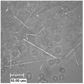 | Figure 1. The electronic microscopy image of SnO2 nanowires |
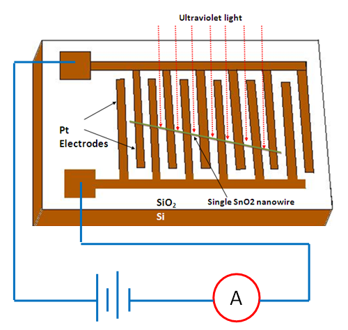 | Figure 2. Schematic diagram of the fabricated photodetector based on a single nanowire SnO2 |
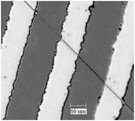 | Figure 3. Image of the fabricated photodetector based on a single nanowire SnO2 |
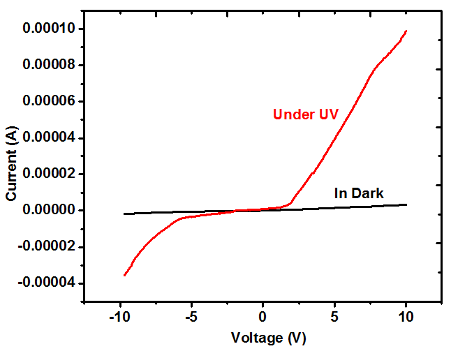 | Figure 4. I-V characteristics of the fabricated photodetector based on a single nanowire SnO2 in dark and under UV light |
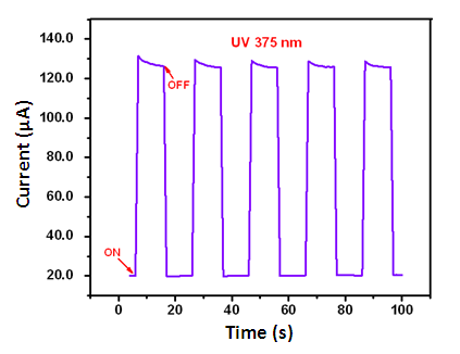 | Figure 5. Photoresponse characteristics of a single SnO2 nanowire photodetector with a 375 nm illuminating UV |
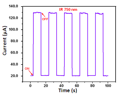 | Figure 6. Photoresponse characteristics of a single SnO2 nanowire photodetector with a 750 nm illuminating IR |
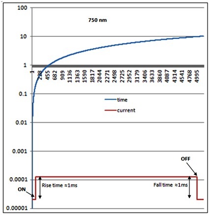 | Figure 7. Enlarged view of a single ON/OFF cycle |
4. Conclusions
- In conclusion, we have fabricated the highly sensitive and ultrafast UV/IR photodetectors based on single SnO2 nanowire. We have successfully synthesized SnO2 nanowires via chemical vapor deposition method. I–V curves under dark and light response were studied. Upon UV/IR illumination, the UV/IR photodetectors based on single SnO2 nanowire exhibits high sensitivity under (UV 375 nm and IR 750 nm) illumination light with low voltage bias 5V at room temperature in the air atmosphere, fast response and recovery time. It also has perfect stability and reliability.
ACKNOWLEDGEMENTS
- The authors gratefully acknowledge financial support of NSF China 61131004.
References
| [1] | Aziz et al., “Seed/catalyst-free vertical growth of high-density electrodeposited zinc oxide nanostructures on a single-layer graphene,” Nanoscale Research Letters, 2014, vol. 9, Article ID 95. |
| [2] | Liwen Sang et al., “A Comprehensive Review of Semiconductor Ultraviolet Photodetectors: From Thin Film to One-Dimensional Nanostructures,” Sensors, 2013, vol. 13, no. 8, pp. 10482-10518. |
| [3] | M.H. Mamat et al., “Fabrication of an ultraviolet photoconductive sensor using novel nanostructured, nanohole-enhanced, aligned aluminium-doped zincoxide nanorod arrays at low immersion times,” Sensors and Actuators B, 2014, vol. 195, pp.609-622. |
| [4] | Jianfang Wang et al., “Highly Polarized Photoluminescence and Photodetection from Single Indium Phosphide Nanowires,” Science, 2001, vol. 293, no. 1455. |
| [5] | Xing J et al., “High sensitive and ultrafast UV photodetector based on ZrO2 single crystals,” China Science. Physics, Mechanics & Astronomy, 2011, vol. 54, no. 8, pp. 1416–1419. |
| [6] | Yanjun Zhang et al., “High performance ultraviolet photodetectors based on an individual Zn2SnO4 single crystalline nanowire,” Journal of Materials Chemistry, 2010, vol. 20, pp. 9858–9860. |
| [7] | Chen Yang et al., “Single p-Type/Intrinsic/n-Type Silicon Nanowires as Nanoscale Avalanche Photodetectors,” NANO LETTERS, 2006, vol. 6, no. 12, pp. 2929-2934. |
| [8] | Kamran ul Hasan et al., “Single nanowire-based UV photodetectors for fast switching,” Nanoscale Research Letters, 2011, vol. 6, Article ID 348. |
| [9] | Yanru Xie et al., “High-performance self-powered UV photodetectors based on TiO2 nano-branched arrays,” Nanotechnology, 2014, vol. 25, Article ID 075202. |
| [10] | Peicai Wu et al., “Fast-speed and high-gain photodetectors of individual single crystalline Zn3P2 nanowires,” Journal of Materials Chemistry, 2011, vol. 21, Article ID 2563. |
| [11] | Jyh-Ming Wu et al., “Ultraviolet photodetectors made from SnO2 nanowires,” Thin Solid Films, 2009, vol. 517, pp. 3870–3873. |
| [12] | Kai Huang et al., “Ultraviolet Photoconductance of a Single Hexagonal WO3 Nanowire,” Nano Research, 2010, vol. 3, pp. 281–287. |
| [13] | A. Maharjan et al., “Room temperature photocurrent spectroscopy of single zincblende and wurtzite InP nanowires,” APPLIED PHYSICS LETTERS, 2009, vol. 94, Article ID 193115. |
| [14] | Zhi-Min Liao et al., “Effect of surface states on electron transport in individual ZnO nanowires,” Physics Letters A, 2007, vol. 367, pp. 207–210. |
| [15] | Q. H. Li et al., “Adsorption and desorption of oxygen probed from ZnO nanowire films by photocurrent measurements,” APPLIED PHYSICS LETTERS, 2005, vol. 86, Article ID 123117. |
| [16] | Cheng-Hsiang Kuo et al.,” High sensitivity of middle-wavelength infrared photodetectors based on an individual InSb nanowire,” Nanoscale Research Letters, 2013, vol. 8, Article ID 327. |
| [17] | N.H. Al-Hardan et al., “Investigation on UV photodetector behavior of RF-sputtered ZnO by impedance spectroscopy,” Solid-State Electronics, 2011, vol. 55, pp. 59–63. |
| [18] | J. Hu et al., “Laser-Ablation Growth and Optical Properties of Wide and Long Single-Crystal SnO2 Ribbon,” Advanced Functional Materials, 2003, vol. 13, no. 493, pp. 493–496. |
| [19] | B. Cheng et al., “Large-Scale, solution-phase growth of single-crystalline SnO2 nanorods,” Journal of the American Chemical Society, 2004, vol. 126, no. 19, pp 5972–5973. |
| [20] | Hyoun Woo Kim and Seung Hyun Shim, "Synthesis of Tin-Oxide One-Dimensional Nanomaterials and Their Characteristics," Journal of the Korean Physical Society, 2005, vol. 47, no. 3, pp. 516-519. |
| [21] | Taekyung Lim et al., "Direct growth of SnO2 nanowires on WOx thin films," Nanotechnology, 2012, vol. 23, Article ID 485702. |
| [22] | Hongtao Huang et al., “Needle-like Zn-doped SnO2 nanorods with enhanced photocatalytic and gas sensing properties,” Nanotechnology, 2012, vol. 17, Article ID 105502. |
| [23] | Suhua Luo et al., “Synthesis and low-temperature photoluminescence properties of SnO2 nanowires and nanobelts,” Nanotechnology, 2006, vol. 23, Article ID 1695. |
| [24] | Hwansoo Kim et al., “Direct growth of oxide nanowires on CuOx thin film,” Nanotechnology, 2012, vol. 23, Article ID 045604. |
| [25] | J.X. Zhou, M.S. Zhang, J.M. Hong, Z. Yin, Solid State Communications, Volume 138, Issue 5, May 2006, Pages 242–246. |
| [26] | Abdelrahim Ate et al., “Ultrahigh responsivity UV/IR photodetectors based on pure CuO nanowires,” AIP Conf. Proc. 1586, 92 (2014), doi:10.1063/1.4866737. |
| [27] | A. Maharjan et al., “Zn2GeO4 and In2Ge2O7 nanowire mats based ultraviolet photodetectors on rigid and flexible substrates,” Optics Express, 2012, vol. 20, no. 3, pp. 2982-2991. |
| [28] | Yaonan Hou et al., “Annealing Effects of Ti/Au Contact on n-MgZnO/p-Si Ultraviolet-B Photodetectors,” IEEE TRANSACTIONS ON ELECTRON DEVICES, 2013, vol. 60, no. 10, pp. 3474-3477. |
| [29] | Mengyu Chen et al., “Fast, Air-Stable Infrared Photodetectors based on Spray-Deposited Aqueous HgTe Quantum Dots,” Advanced Functional Materials, 2014, vol. 24, pp. 53–59. |