-
Paper Information
- Next Paper
- Paper Submission
-
Journal Information
- About This Journal
- Editorial Board
- Current Issue
- Archive
- Author Guidelines
- Contact Us
International Journal of Optoelectronic Engineering
p-ISSN: 2167-7301 e-ISSN: 2167-731X
2013; 3(1): 1-5
doi:10.5923/j.ijoe.20130301.01
Preparation and Properties of Cu4SnS4 Thin Films
 Abstract
 Reference
 Full-Text PDF
 Full-text HTML
V. P. Geetha Vani1, R. W. Miles2, K. T. Ramakrishna Reddy1
1Department of Physics, Sri Venkateswara University, Tirupati, 517502, India
2School of CEIS, Northumbria University, Newcastle, NE1 8ST, U. K
Correspondence to: K. T. Ramakrishna Reddy, Department of Physics, Sri Venkateswara University, Tirupati, 517502, India.
| Email: |  |
Copyright © 2012 Scientific & Academic Publishing. All Rights Reserved.
The ternary semiconductor, copper tin sulphide (Cu4SnS4) is considered to be a promising absorber layer in the development of thin film heterojunction solar cells due to its optimum physical properties. Further, it contained more abundant and cheaper elements that are environmentally safe to handle. In the present study, Cu4SnS4 (CTS) films were deposited by co-evaporation technique at various deposition temperatures in the range 200 – 350℃. The effect of substrate temperature (Ts) on the growth of CTS films was investigated. The structure, composition, morphology and optical properties of the films were studied using appropriate techniques. The X-ray diffraction analyses revealed that all the deposited films were polycrystalline and showed the (221) plane as the preferred orientation. The energy dispersive spectroscopy analysis indicated all the three elements, Cu, Sn and S. The grain size of the films was varied in the range 180 – 350 nm. The average optical transmittance of the films was found to be ~ 80% in the visible region and the evaluated optical band gap of the films increased from 1.70 eV to 1.93 eV with the increase of substrate temperature.
Keywords: Cu4SnS4 Films, Co-Evaporation, Structure, Optical Properties
Cite this paper: V. P. Geetha Vani, R. W. Miles, K. T. Ramakrishna Reddy, Preparation and Properties of Cu4SnS4 Thin Films, International Journal of Optoelectronic Engineering, Vol. 3 No. 1, 2013, pp. 1-5. doi: 10.5923/j.ijoe.20130301.01.
Article Outline
1. Introduction
- Polycrystalline thin film solar cells using CuInGaSe2 (CIGS) and CdTe as absorber materials have proved to be potential candidates for photovoltaic solar cell fabrication with the demonstrated efficiencies>15%[1, 2]. Although solar cell modules based on these materials are commercially available in the market, however, these cells are facing few serious problems that might cloud their prospects in the future. The availability of In and Ga in the case of CIGS and the toxicity of Cd in CdTe-based cells are considered to be the detractors of these technologies for large scale production of the modules with more public acceptability. Therefore, attention of researchers is diverted towards the investigation of novel and new photovoltaic materials that are freely available in nature at low cost and likely to replace these front runner materials in the future. Among the many materials that have been studied in recent years, the ternary semiconductor, copper zinc tin sulphide (CZTS) is proved to be an important alternative with the conversion efficiencies > 10%[3, 4]. But it is a quaternary material where the elements involved had a large variation in the vapor pressures. A ternary or binary compound with similar properties to CZTS will be more useful. In this context, copper tin sulphide (CTS) is considered to be one of the potential materials as an absorber layer in solar cells because of its optimum physical properties such as energy band gap and optical absorption coefficient[5, 6]. Further, it contained more abundant and cheaper elements that are environmentally safe to handle. Moreover, the investigations reported on the deposition and characterization of copper tin sulphide layers is very meager. Copper-tin-sulphide system exists in different stable forms and the prominent of them are: Cu2SnS3 with the disordered cubic structure and Cu4SnS4 that exists in orthorhombic structure[7]. The present investigation is aimed to deposit Cu4SnS4 (CTS) films by a simple co-evaporation technique using CuS and SnS as precursors. The composition, structure and optical properties of the grown films were studied in relation to the substrate temperature and the results discussed.
2. Experimental Details
- Thin films of copper tin sulphide were formed on glass substrates by vacuum co-evaporation technique. A Hind Hi Vac Box Coating system was used for the deposition of the films at a vacuum better than 10-5 Torr. 5N pure SnS powder and CuS were used as the starting materials to grow the films. The materials were taken in two tantalum boats connected to two separate heating sources. The boats were covered with quartz wool in order to avoid splattering of the materials. The temperatures of both SnS and CuS sources were maintained at the predetermined values for the evaporation to occur. After getting the required evaporation rate, the two shutters over the sources were moved sideways for the deposition to take place. Ultrasonically cleaned Corning glass was used as the substrates. The layers were deposited at various substrate temperatures (Ts) that vary in the range, 200–350℃. The source-substrate distance was maintained as 20 cm. The as-grown layers were characterized to evaluate the chemical and physical properties using appropriate techniques and procedures. Philips X-ray diffractometer with Cu kα radiation (λ=1.542 A) was used to analyze the structural properties of the films such as the crystal structure, preferred orientation, crystallite size and texture coefficient. The X-ray diffraction (XRD) spectra were recorded in the 2θ range, 20-70. The chemical composition of the films was measured using Energy dispersive X-ray analyzer (Inca Penta FETx3) attached to scanning electron microscope (SEM). The surface topology and grain size of the films were investigated using Zeiss SEM. The optical properties such as the transmittance, reflectance, absorption coefficient and energy band gap were determined using Perkin Elmer UV-Vis-NIR spectrophotometer. In this study, the thickness of the films was measured using the quartz crystal thickness monitor present in the vacuum system and it was approximately 200 nm.
3. Results and Discussion
- The visual observation of the as-grown CTS layers indicated that the films were reddish brown in colour, pin hole free and uniform. The scratch tape test revealed that the film were strongly adherent to the surface of the substrate. The energy dispersive X-ray analysis data revealed that all the layers grown at different substrate temperatures consisted of copper, tin and sulphur with small amount of carbon. The presence of C might be due to the oil vapours from the diffusion pump. Figure 1 shows a typical EDAX spectrum of CTS fil deposited at 350℃. The films formed at higher substrate temperatures >300℃ showed slight deficiency of S compared to other elements. This might be due to its re-evaporation because of the high vapour pressure. The EDAX analysis also indicated that the composition of various elements was nearly stoichiometric for the films formed at 300℃. CTS films deposited at other substrate temperatures have shown compositional deviation from the stoichiometric value.
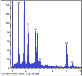 | Figure 1. EDAX spectrum of CTS film formed at 350℃ |
 | (1) |
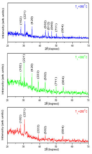 | Figure 2. X-ray diffraction spectra of CTS films grown at various temperatures |
 | (2) |
 | (3) |
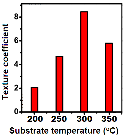 | Figure 3. Variation of texture coefficient with substrate temperature |
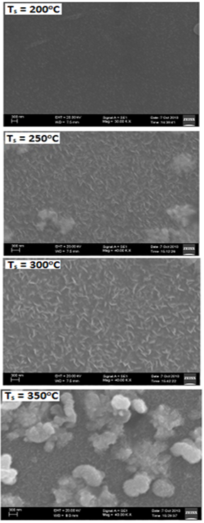 | Figure 4. SEM photographs of CTS films formed at different substrate temperatures |
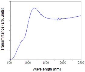 | Figure 5. Optical transmittance versus wavelength spectrum of CTS films grown at Ts=300℃ |
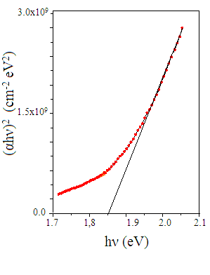 | Figure 6. (αhν)2 versus hν plot for CTS film formed at Ts=300℃ |
 | (4) |
 | (5) |
4. Conclusions
- Thin films of Cu4SnS4 have been deposited by co-evaporation method. The films were formed on Corning glass substrates at different temperatures varying from 200℃ to 350℃. The layers formed at 300℃ showed nearly stoichiometric composition. All the grown films were polycrystalline with the (211) plane as the dominant orientation and the cyrstallinity of the films increased with the increase of substrate temperature. The films formed at substrate temperatures > 250℃ had an optical transmittance > 60%. The films exhibited an absorption coefficient > 104 cm-1 and the evaluated energy band gap varied in the range, 1.70 – 1.94 eV.
ACKNOWLEDGEMENTS
- One of the authors (V.P. Geetha Vani) would like to thank UGC for awarding RFSMS Fellowship. Prof. K. T. R. Reddy, Prof. R. W. Miles, Sri Venkateswara University and Northumbria University acknowledge financial support from European commission via Marie-Curie funding.