Faria L. A.1, Nohra L. F. M.1, Gomes N. A. S.2, Alves F. D. P.3
1Instituto Tecnológico de Aeronáutica São José dos Campos , Brasil
2Universidade Estadual de Campinas, Campinas , Brasil
3Naval Postgraduate School Monterey , California , USA
Correspondence to: Nohra L. F. M., Instituto Tecnológico de Aeronáutica São José dos Campos , Brasil.
| Email: |  |
Copyright © 2012 Scientific & Academic Publishing. All Rights Reserved.
Abstract
Nowadays, the detection in the infrared band (IR) has shown great importance in several areas such as skin illnesses detection, remote sensor and in different military devices. The responsible for such detection is, basically, photodetector arrays (FPA) sensitive to infrared radiation. This paper presents a modular and adaptative test-bed, based upon an arrangement of 24 electro and optical components divided in four major functional blocks, providing methodological procedures that allows an accurate design verification of infra-red photodetectors. The target metric that the system is conceived to provide is Responsivity. In essence, the developed system differs from the previous ones by its adaptability and its hardware modularity conception that allows an easy reconfiguration to test different kinds of photodetectors. Here we compare a theoretical calculation of responsivity with actual experimental measurements, allowing low temperature measurements between 16K and 100K, in wavelength from 0.7μm up to 12μm (0.8μm to 1.0μm in this work) and the possibility to set detectors with up to 10 I/O electric terminals. The operational validation of this test-bed is achieved with a studied Quantum Well Infrared Photodetectors (QWIP), exhibiting high compliance with the expected theoretical results.
Keywords:
Design Verification, Spectroscopy, Adaptative Test-Bed
1. Introduction
Nowadays, the detection in the infrared band (IR) has shown great importance in several areas such as skin illnesses detection, remote sensor and in different military devices[1][2]. The responsible for such detection is, basically, photodetector arrays (FPA) sensitive to infrared radiation. Those devices are able to reproduce a target scene and their resolution depends on the number of sensible elements. There is different kind of photodetectors, each one presenting special features that allows them to be implemented in typical applications. Therefore, there is no single type of photodetector that is useful in all kinds of applications. Each kind of application demands a most appropriate sensor[3].Infrared radiation is a form of electromagnetic radiation with wavelengths ranging from just under one micrometer to about one millimeter in length. This region is further subdivided, depending on the atmospheric transmittance window, into the near infrared (0.7-3μm), mid-wavelength infrared (3-6μm), long-wavelength infrared (6-15μm), and Terahertz (1012Hertz) regions. Within these regions, atmospheric absorption due to water, CO2, and other airborne molecules limit the ranges[3]. In order to reduce this effect, infrared detectors have to be optimally designed within ranges where transmittance shows to be as great as possible.Such a design requires methodological, repeatable and operational testing of the photodetector, under controlled conditions. Focusing this main goal, it is presented a modular and adaptative test-bed for photodetectors in the range of 0.7μm to 12μm. With simple and quick modifications, it is possible to reconfigure the setup in order to optimize the testing of the detector-under-test (DUT) and acquire adequate parameters to evaluate its performance and feedback the design process. An infrared sensor performance can be evaluated by some Figures of Merit, which the most important ones are Responsivity and Dark Current. The performance metric provided in this work is Responsivity, through the so called Photocurrent Spectroscopy Method[4].The Electronic Warfare Laboratory (LabGE), in Instituto Tecnológico de Aeronáutica (ITA), in , has a research area in the development of Photodetectors. Some samples of different QWIPs are being characterized using the proposed test-bed, in order to feedback the design processes and improve the devices performance. Furthermore, with the presented setup, it is possible to evaluate, not only this kind of detectors (QWIPs) but also other ones, like those embedded in missiles, thermal cameras and a number of options. This study helps us to understand the behaviour of the responsivity in different temperatures and bias voltage which is used in back-of-the-envelope calculations in Infrared Photodetectors designs.
2. QWIPs Responsivity
QWIPs are sensors that perform the detection in the IR range by the photons absorption in quantum-wells of semiconductor material[5]. As photoconductive detectors, its operation is dependent on the application of a bias voltage. The detection occurs from the photo excitation of electrons, or holes, existing in ground states or in the excited states of the valance and conduction bands[5]. Through an adequate material selection, it is possible, controlling its composition, size and applied bias, to predict the absorption spectrum of the device[5]. Among the infrared photodetectors, the QWIPs show significant advantages over the other ones, because of their multi-spectral detection, ultra-fast responses, large number of elements arrays (Megapixels), high reproducibility, low cost and special detection to specific target signatures[6]. Designing and producing QWIPs is a complex process that relies heavily on cutting-edge semiconductor growth techniques and on the existing design support softwares. Due to the intricacy of their design, it is important to probe its Response characteristics in order to validate the designing methods.A. ResponsivityThe Responsivity R is defined as the ratio between the photocurrent IP and the power of incident radiation Φ0 (photon flux) for each wavelength. Therefore, it cannot be measured directly. However, it is possible to measure both the photocurrent of a detector due to an applied bias voltage and the photocurrent generated by another photodetector with a known responsivity, when subject to the same incident radiation power. This last detector is known as “Reference detector”. Thus, IP can be calculated by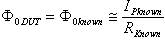 | (1) |
and 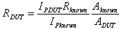 | (2) |
where DUT refers to detector-under-test, known refers to the reference detector and A is the area of the detectors.This method is known as “Comparison Method” and is the basis for the developed test-bed of this work. The Photocurrent Spectroscopy is a technique that allows the measuring of the photocurrent generated by aphotodetector for each wavelength IP(λ). Through the absorption of electromagnetic radiation it is possible to identify the bandwidth detection, peak responsivity, peak detectivity and the amplitude of the photocurrent generated by a detector[3]. The photocurrent varies with the applied electric field, F, the temperature, T, doping levels and the characteristics of the quantum wells (number of wells, distance and width)[7] and can be represented, in a simplified way for QWIPs, where αLW<<1 (majority of the current cases) by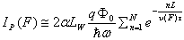 | (3) |
where α is the absorption coefficient, Φ0 is the incident photon flux power, L is the period of multiple quantum wells, LW is the width of the well, N is the number of wells, n represents the nth structure well, υ(F) is the drift velocity as a function of the external applied electric field (F) and τ is electron life-time.The dependence of the Responsivity, and the photocurrent, to the Bias Voltage and to the Temperature, besides de verification of the absorption peaks and the bandwidth will be the goals of this work.
3. Test-Bed Arrangements
The conceived system comprises a collection of 24 electro and optical components, from 9 different manufacturers, integrated together under a photocurrent spectroscopy methodology. In order to obtain a yield consistent with the desired measurements and truthful results, each one of these components had to be understood and characterized, because the more components necessary to a setup, the greater the probability of being introduced additional deficiencies to the system. All of them were selected to ensure optimum performance in all regions and a broad-spectrum coverage. They are arranged as illustrated on Fig.1.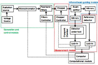 | Figure 1. Block diagram of the test-bed arrangements |
In Fig.1, it can be seen that the components are arranged in 4 major blocks, by functional similarity. They are:• Generation and control module;• Infrared beam guiding module;• Measurement module; and• Computational module.Each one of them has a specific function and will be described from now on.A. Generation and control moduleThis first module is responsible for providing narrow bandwidth energy, known wavelength and high spectral purity. It is the most important block of the arrangement, because of its high adaptability and simplicity of changes, making it functional for the wide range of infrared photodetectors.The components of this module include two voltage sources, two radiation sources in the infrared band, a monochromator equipped with three diffraction gratings and micrometer driven apertures, a filter wheel assembly with 5 filters and a chopper-wheel that modulates the output energy at a known and fixed frequency. This last component can be considered also as a part of the measurement module.In order to operate all over the desired range of infrared band (0.7μm to 12μm) and meet the design requirements for testing, it was required to include two energy sources, a Tungsten-Halogen Lamp and a Silicon-Carbide Bar. The changing from one to the other is made in an easy way, in order to better fit the radiation to each one of the detectors under test. The control of each source is accomplished through a voltage source that allows meeting the operating requirements.The Tungsten-Halogen Lamp (NEWPORT®6333) is a light bulb that produces radiation when electric current passes in its filament. It is composed of a Tungsten filament immersed in a halogen gas atmosphere. Considering the Planck’s Radiation Law[8], this kind of lamp is a grey body, emitting a well-defined spectrum and proportional to the blackbody. Its relative spectral radiance can be seen in Fig.2 on the basis of wavelength.The Silicon-Carbide Bar (NEWPORT®6363) is an excellent source of infrared radiation between 1.5μm and 15μm. It presents the same features of the Tungsten-Halogen Lamp, showing grey body behaviour. Its relative spectral radiance can be seen in Fig.2 on the basis of wavelength.Table 1. Diffraction gratings implemented on the test-bed
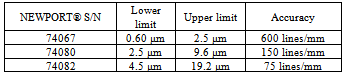 |
| |
|
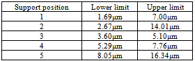
Once the generation in broadband is achieved with only two sources, instead of multiple ones, it is desirable, after the source selection, to sweep the spectrum in a controlled way in order to generate the necessary data. Therefore, it is implemented the monochromator “Cornerstone 260 (NEWPORT®74125)” that, with two parabolic mirrors and a diffraction grating, allows the separation of the incident radiation at wavelengths with high resolution, less than 1nm. This instrument presents three grating possibilities, depending on the desired performance. The lower and upper measurements limits and the number of lines per millimetre are basic parameters to be chosen before the grating selection. The changing of each one of these gratings is made in an easy way, making possible to best fit the DUT testing. The options of diffraction gratings established to this test-bed can be seen in Table 1.The monochromator alone cannot achieve the desired spectral purity when a broad-spectrum energy is incident on the diffraction grating, because of the higher orders of diffraction. With multiple wavelengths incident on the grating, some number of wavelengths will be diffracted at the same given angle. Since only the grating cannot respond to the incident energy in an adequate way, the best approach to improving the spectral purity of the diffracted energy is to restrict the bandwidth of the incident energy, what is done with pass-band filters.Five pass-band filters were selected based on the possible wavelengths of interest. The absorption of energy with wavelengths smaller and higher than those, avoid the appearance of unwanted high order contributions and improved the spectral purity of the monochromator output. These filters are positioned in the signal path with a computer-controlled wheel. This computational selection makes it easier to choose and set the right filter to be employed in each case of testing. The options of available filters to this test-bed can be seen in Table 2.Table 2. Filters implemented on the test-bed
 |
| |
|
The satisfactory adjustment of the components of this module, is the real improvement provided by this test-bed. Adjusting three different components (radiation sources, monochromator gratings and pass-band filters) it is possible to select the right wavelengths to be generated and swept, testing the DUT with high accuracy. A summary of this module information can be seen, graphically, on Fig.2.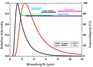 | Figure 2. Summary of the arrangements of Module 1 |
Based on Fig.2, one can see that, varying the emitting source and the type of filter, besides the diffraction grating, it is possible to select a particular band of the spectrum, what is done easily and quickly with this test-bed. B. Infrared beam guiding moduleThis module is responsible for directing the energy from the generation module to the detectors. Once the desired wavelengths left the monochromator and are modulated by a chopper, it has to be routed to a beam splitter. It is done by a parabolic reference mirror that collimates the beam. Then, the beam splitter reflects different amounts of energy to each side, being transmitted, via two more parabolic mirrors, to the detectors (reference detector and DUT), granting that both will receive equal quantity of radiation. The difference in the radiation directed to the reference detector and to the DUT must be sufficient to compensate the existing interfaces in their optical path. In this phase, the beam splitter positional changes are essential, in order to grant equal radiation and optimum focusing of the image on both detectors. The most important element of this module is the Beam Splitter (EDMUND OPTICS® NT – 47006), which is silver made and presents a 98% of reflectance. Its adjustment is handmade and the total power directed to each side must be previously calculated, in order to grant equal quantities of radiation power on each detector. This calculation is presented below.For the other mirrors, it is important to have an adequate positioning of the elements, where the focal distances knowledge is essential.C. Measurement moduleThis module includes a reference detector, the detector-under-test (DUT) and the respective lock-in amplifiers. The lock-in amplifiers STANFORD RESEARCH®830 (SR830) are incorporated into the system for their ability to significantly improve the signal-to-noise ratio. A lock-in amplifier is designed to rely on A/C techniques (signal processing) to measure DC or slowly varying signals and is able to amplify currents up to 2fA. In order to employ a lock-in amplifier, the signal to be measured must be modulated at a known, fixed frequency while noise sources remain non-modulated. In this test-bed, an optical chopper is used to interrupt the beam exiting from the monochromator at a fixed frequency, and is located just after the monochromator and the pass-band filters. The lock-in, chopper and pass-band filters are synchronized in order to reject the noise outside the designed pass-band and increase signal to noise ratio.During the generation of the radiation, in the first module, variations are inherent in the efficiency of optical components. Therefore, the incident energy at the DUT could not be considered constant for different wavelengths. Thus, the only way to verify the amount of energy incident on the DUT is to measure it, and it could be done by sending the same quantity of energy to another detector with known and flat response. This device is called “reference detector”.The reference detector is a thermopile and consists of a set of 36 thermocouples. The increasing in temperature generates a potential difference, which is measured based on thermoelectric effect.On the other hand, the detector-under-test (DUT) must be subject to an equal radiation intensity to the reference detector, in order to compare the photocurrents and derive its Responsivity. This calculation can be made through the following equations, preserving the components parameters.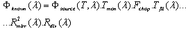 | (4) |
and | (5) |
where Φknown is the power in the reference detector, Φsource is the power of the radiation source, Tmon is the transmittance of the monochromator, Fchop is transfer factor of the chopper, Tfil is the transmittance of the filters, Rmirr is the reflectance of the parabolic mirror, Rdiv is the reflectance of the beam splitter, Twindow is the transmittance of the cryogenic chamber window and Tsubst is a transmittance of the substrate of the detector. All of these parameters and components have to be characterized before the final arrangements for the detector testing, in order to a correct evaluation of the incident radiation.These two equations allow concluding that there are two more components in the optical path of the detector under test than that of the reference detector. Then, when the beam passes through the beam splitter, this factor must be taken into account. This assertion is valid only for detectors that require measurements at low temperatures.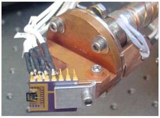 | Figure 3. Photodetector holder, DUT and the 10 I/O electric signals bus |
A very specific case in photodetectors is the measuring at low temperatures. For these cases, it is implemented a controlled temperature environment, which permits measurements up to 10K. This environment is designed by HELIX Technology Corporation and is composed by 4 equipments: a vacuum pump, a Helium compressor, a temperature controller and cryogenic chamber. The vacuum pump provides pressures up to 10-3 torr., avoiding condensation of water molecules inside the chamber. The Helium compressor CTI-Cryogenics® Model 8200 (K08817640) provides, in a closed cycle and two stages, freezing the temperature to 10K. Finally, the temperature controller, LAKESHORE® Model 325 (3250518), provides the environment heating through electric resistances, and a measurement system made by silicon diodes. Inside the cryogenic chamber it was fixed a holder to the detectors and a bus with 10 I/O electric terminals, providing the injection and measurements of the 10 I/O signals. This special bus is made with low resistance wires (0.4 Ω/km @ 20º C) in order to avoid significant losses in the signals and can be seen on Fig.3.D. Computational moduleThe fourth module is comprised of the computer, its software and communication cables. It is not fully implemented yet and its software realizes, until now, only the monochromator and Lock-in controls. Future works will integrate all the functions and provide a single operator control panel for the photoconductor testing. Graphics displaying the responsivity versus wavelength and an output file in .CSV or .TXT format are also a future goal.
4. Operational Validation
As a way to validate the proposed arrangement, it was used a QWIP designed by[6] and already studied and calculated by[9]. The great benefit of testing this device is its already calculated absorptions peaks for each one of the allowed inter-band transitions. Two measurements in the Near Infrared (NIR) photodetector were carried. The first one maintaining a constant temperature (16K) and varying the bias voltage. The second one is made with a constant bias voltage (1.5V) and a variable temperature (from 16 to 60K). These kinds of testing allow validating the sensibility of the photocurrent to the temperature and bias voltage, beyond measuring the responsivity peak, detection bandwidth and other features of Responsivity for inter-band transitions. A number of other kind of infrared detectors can be tested with similar procedures, finding these features and other ones for intersubbands transitions. 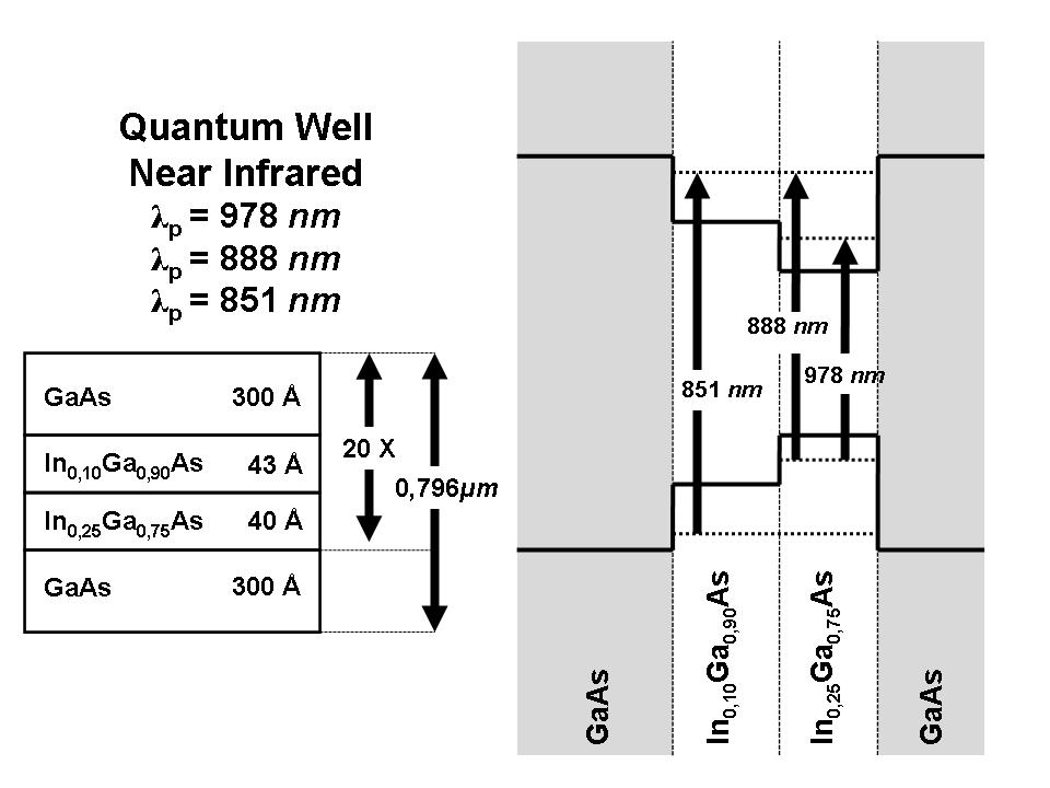 | Figure 4. Structure of the detector under test and the theoretical allowed transitions |
The transfer matrix method (TMM) is used to predict the responsivity of QWIP based in interband and intersubband transitions. The absorption peaks previously calculated by[9] can be seen in Fig.4, besides the QWIP structure.In order to validate the test-bed, it was performed the Photocurrent measuring, varying the bias voltage and keeping temperature constant in 16K. The results can be seen in Fig.5, through a Responsivity versus wavelength diagram.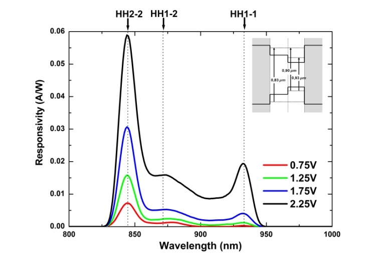 | Figure 5. Responsivity for[8] QWIP-NIR for a constant temperature |
Fig.5 is a typical curve of Responsivity where a high definition is presented (accuracy of 1nm in the wavelength). It is possible to verify the bandwidth of detection, besides the absorption peaks. This kind of experiment is essential to the validation and testing of prototyped devices, in order to feedback the design process and to increment the performance of those detectors. Figure 5 also shows the sensibility of the device in relation to the bias voltage. This is another relevant feature to the designer, when developing the detector. These features are essential for improving the project.It was also carried a test maintaining the bias voltage constant and varying the temperature. The results can be seen on Fig.6.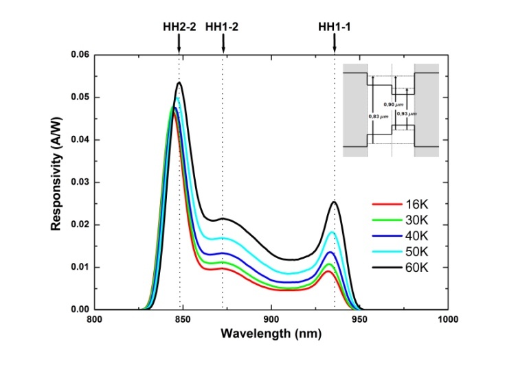 | Figure 6. Responsivity for[8] QWIP-NIR for a constant bias voltage |
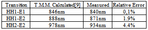
Figure 5 and Fig.6 exhibited the expected behaviour, presenting three peaks of absorption in the same wavelengths previously found and an adequate temperature behaviour, where the higher the temperature, the greater will be the photocurrent, maintaining all the absorption peaks.This result has demonstrated that changes in temperature, between 16K and 60K, have less influence on responsivity than the bias voltage. However, when the temperature increases, the structure presents an absorption peak in a different wavelength. This phenomenon is not observed in the bias variation.Based on Fig.5 and Fig.6, it is possible to see that there are three peaks of absorption, in 840nm, 871nm and 934nm, which correspond to intersubbands transition (heavy hole subband (HH) and electron subband (E)).They agree with the theoretical calculation[9], presenting a relative error less than 5% for all the peaks, which can be seen in Table 3.Table 3. Compare of peaks of absorption calculated[9] and measured
 |
| |
|
The relative error is most likely due to uncertainties in semiconductor parameters such as band gap and junction band offsets. This is due to indium segregation process and its influence on the energy levels and optical properties in InGaAs/GaAS systems[9].Those comparison indicate that TMM is a suitable tool to be used in QWIP design, exhibiting high compliance with the expected theoretical results.
5. Conclusions
A modular and adaptative test-bed for infrared photodetectors, aimed to be an auxiliary tool for designers, rather than a production testing device, has been described. The system comprises 24 electrical and optical components, divided in four major functional blocks, building up a modular and configurable solution to measure Responsivity in a broadband of infrared spectrum. The concept of the test-bed allows low temperature measurements between 16K and 60K, broadband radiation possibilities in wavelength from 0.7μm up to 12μm (0.8μm to 1.0μm in this work) and the possibility to set detectors with up to 10 I/O electric terminals. The operational validation of this test-bed was achieved with an already studied QWIP, exhibiting high compliance with the expected theoretical results, fulfilling the expectations, and showing a great potential to be used to detectors design.
References
| [1] | Itoh, N. et al. Kiso observatory near-infrared camera with a large format array. In: SPIE Infrared Technology, 21., 1995, San Diego. Proceedings… Bellingham: SPIE, 1995. v. 2552, p. 430–437. |
| [2] | Scribner, D. A.; Kruer, M. R.; Killiany, J. M. Infrared focal-plane array technology. Proceedings of the IEEE, v.79, n. 1, p. 66–85, jan. 1991. |
| [3] | NOHRA, L. F. M. Espectroscopia de Fotocorrente Aplicada a Fotodetectores Infravermelhos a Poços Quânticos. 2010. 96 folhas. Tese de mestrado em Engenharia Eletrônica e de Computação – Instituto Tecnológico de Aeronáutica, São José dos Campos. |
| [4] | HANSON N.A., “Characterization an Analysis of a Multicolor Quantum Well Infrared Photodetector”, Tese de Mestrado, Naval Postgraduate School, Monterey, 2006. |
| [5] | SCHNEIDER H., “Quantum Well Infrared Photodetectors, Physics and Applications”, Springer- Verlag, Berlim, 2007. |
| [6] | ALVES F. D. P. Three-band quantum well infrared photodetector using interband and intersubband transitions // Tese de Doutorado. - São José dos Campos : Instituto Tecnológico de Aeronáutica, 2008. - Vol.1. - p. 145. |
| [7] | LEVINE B. F. Quantum-Well Infrared Photodetectors[Journal] // Applied Physics Letters, vol. 78, n. 8. - 1993. - pp. 1-81. |
| [8] | RESNICK H. Física Quântica, Moléculas, Átomos e Partículas[Book]. - Rio de Janeiro : Ed. Campus, 1974. |
| [9] | SANTOS R. A. T. Projeto do Fotodetetores Infravermelhos a Poços Quânticos usando o Método de Matriz de Transferência // Tese de Doutorado. - São José dos Campos : ITA, 2009. - Vol. 1 |
 Abstract
 Reference
 Full-Text PDF
 Full-Text HTML