-
Paper Information
- Previous Paper
- Paper Submission
-
Journal Information
- About This Journal
- Editorial Board
- Current Issue
- Archive
- Author Guidelines
- Contact Us
International Journal of Optoelectronic Engineering
2012; 2(2): 5-11
doi: 10.5923/j.ijoe.20120202.02
Optical and Other Measurement Techniques of Carrier Lifetime in Semiconductors
 Abstract
 Reference
 Full-Text PDF
 Full-Text HTML
Yeasir Arafat , Farseem M. Mohammedy , M. M. Shahidul Hassan
Department of EEE, BUET, Dhaka, 1000, Bangladesh
Correspondence to: Yeasir Arafat , Department of EEE, BUET, Dhaka, 1000, Bangladesh.
| Email: |  |
Copyright © 2012 Scientific & Academic Publishing. All Rights Reserved.
In this paper, various methods for characterization of semiconductor charge carrier lifetime are reviewed and an optical technique is described in detail. This technique is contactless, all-optical and based upon measurements of free carrier absorption transients by an infrared probe beam following electron-hole pair excitation by a pulsed laser beam. Main features are a direct probing of the excess carrier density coupled with a homogeneous carrier distribution within the sample, enabling precision studies of different recombination mechanisms. The method is capable of measuring the lifetime over a broad range of injections (1013-1018 cm-3) probing the minority carrier lifetime, the high injection lifetime and Auger recombination, as well as the transition between these ranges. Performance and limitations of the technique, such as lateral resolution, are addressed while application of the technique for lifetime mapping and effects of surface recombination are also outlined. Results from detailed studies of the injection dependence yield good agreement with the Shockley–Read–Hall theory, whereas the coefficient for Auger recombination shows an apparent shift to a higher value, with respect to the traditionally accepted value, at carrier densities below 2×1017 cm-3. Data also indicate an increased value of the coefficient for bimolecular recombination from the generally accepted value. Measurement on an electron irradiated wafer and wafers of exceptionally high carrier lifetimes are also discussed within the framework of different recombination mechanisms.
Keywords: Carrier Lifetime, Electron-Hole Pair, Shockley–Read–Hall Recombination, Generation
Article Outline
1. Introduction
- With the decrease in feature size in semiconductor manufacturing, molecular contamination problems are increased significantly[1]. Recombination lifetime as well as diffusion length measurements have become ubiquitous in the semiconductor industry, because they are a good indicator of wafer contamination[2]. When the defect densities in semiconductors are low, lifetime is one of few parameters that gives significant information about the lower concentration. No other technique can detect defect densities as low as 109–1011 cm−3 in a simple, contactless room temperature measurement. In principle, there is no lower limit to the defect density determined by lifetime measurements[3]. It is for these reasons that the IC industry, largely concerned with unipolar MOS devices in which lifetime plays a minor role, has adopted lifetime measurements as a “process cleanliness monitor”[4]. Alongside this, recombination and generation lifetime as well as measurements of carrier diffusion lengths in semiconductors are also very crucial for photovoltaic devices[5] which have recently become very attractive topic to researchers.The theory of electron-hole pair recombination through recombination centers (traps) was put forth in 50s of the last century in the well-known works by Shockley-Read-Hall (SRH)[6,7]. Here, we discuss lifetimes, their dependence on semiconductor material and device parameters like energy level, injection level & surfaces and how lifetimes are measured. Different measurement methods can give widely differing lifetimes for the same material or device. In most cases, the reasons for these discrepancies are fundamental and are not due to a deficiency of the measurement. The difficulty with defining a lifetime is that we are describing a property of a carrier within the semiconductor rather than the property of the semiconductor itself.
2. Theory
- There are two principal categories of carrier lifetimes: recombination lifetimes and generation lifetimes. The concept of recombination lifetime τr holds when excess carriers decay as a result of recombination. Generation lifetime τg applies when there is a paucity of carriers, as in the space- charge region of a reverse-biased device and the device tries to attain equilibrium. During recombination an electron-hole pair ceases to exist on average after a time τr, illustrated in Fig. 1(a). The generation lifetime, by analogy, is the time that it takes on average to generate an ehp, illustrated in Fig. 1(b). Thus generation lifetime is a misnomer, since the creation of an ehp is measured and generation time would be more appropriate. Nevertheless, the term “generation lifetime” is commonly accepted. When these recombination and generation events occur in the bulk, they are characterized by τr and τg. When they occur at the surface, they are characterized by the surface recombination velocity sr and the surface generation velocity sg, also illustrated in Fig. 1. Both bulk and surface recombination or generation occur simultaneously and their separation is sometimes quite difficult. Consisting of bulk and surface components, the measured lifetimes are always effective lifetimes.It is instructive to consider τr and τg in more detail before discussing lifetime measurement techniques. The excess ehps may have been generated by photons or particles of energy higher than the band gap or by forward biasing a pn junction. There are more carriers after the stimulus than before and the excess carriers return to equilibrium by recombination.
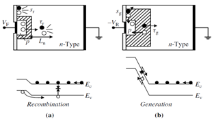 | Figure 1. Illustration of various recombination and generation mechanisms for a (a) forward-biased and (b) reverse-biased junction |
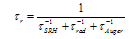
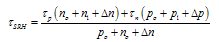
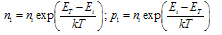
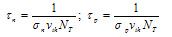
2.1. Recombination Lifetime and Surface Velocity
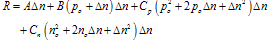
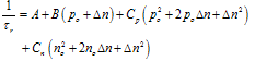
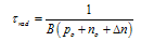
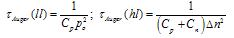
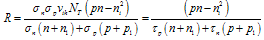
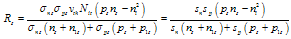
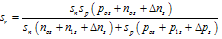
- The departure of the carrier densities from their equilibrium values non-linearly controls the bulk recombination rate R. We consider a p-type semiconductor throughout this work and are chiefly concerned with the behavior of the minority electrons. Confining ourselves to linear, quadratic, and third order terms, R can be written as
 | (1) |
 | (2) |
 | (3a) |
 | (3b) |
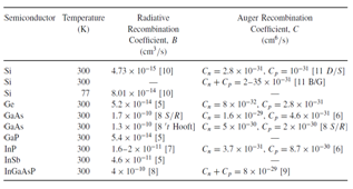
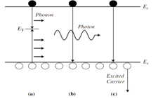 | Figure 2. Variuos mechanisms: (a) SRH (b) radiative and (c) Auger |
 | (4) |
 | (5) |
 | (6a) |
 | (6b) |
 | (7) |
 | (8) |
|
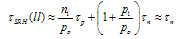
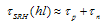
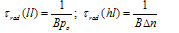
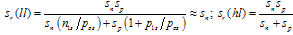
2.2. Recombination Lifetime and Level of Injections
- Equations (5) to (8) simplify for both low-level and high-level injection. Low-level injection holds when the excess minority carrier density is low compared to the equilibrium majority carrier density, Δn<<po. Similarly, high- level injection holds when Δn>>po. The injection level is important during lifetime measurements. The appropriate expressions for low-level (ll) and for high-level (hl) injection become
 | (9) |
 | (9a) |
 | (10) |
 | (11) |
 | (12) |
 | (13) |
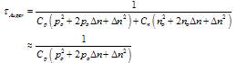
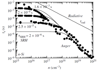 | Figure 3. Recombination lifetime versus majority carrier density for n-Si with Cn = 2 × 10⁻³¹ cm6/s and B = 4.73 × 10⁻¹⁵ cm3/s |
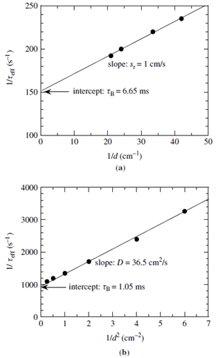 | Figure 4. Determination of bulk lifetime, surface recombination velocity and diffusion coefficient from lifetime measurements. Data from [10] |
 | (14a) |
 | (14b) |
 | (15) |
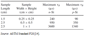
2.3. Recombination Lifetime Measurements Techniques
- Recombination lifetime can be measured optically or electrically. The commonly used techniques are1) Optical Measurements: Photoconductance Decay (PCD), Quasi-Steady-State Photoconductance (QSSPC), Short-Circuit Current/Open-Circuit Voltage Decay (SCCD/ OCVD), Photoluminescence Decay (PLD), Surface Photovoltage (SPV), Steady-State Short-Circuit Current (SSSCC), Free Carrier Absorption, Electron Beam Induced Current (EBIC) etc.2) Electrical Measurements: Diode Current-Voltage, Reverse Recovery (RR), Open-Circuit Voltage Decay (OCVD), Pulsed MOS Capacitor, Other Techniques.
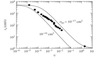 | Figure 5. The surface recombination velocity sr versus injection level η as a function of σps for Nit = 1010 cm−2, pos = 1016 cm−3, ETs = 0.4 eV, σns = 5 × 10⁻¹⁴ cm2. Data from [11] |
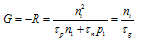
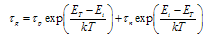
2.4. Generation Lifetime and Surface Velocity
- Every recombination process of Fig. 2 has a generation counterpart. The inverse of multiphonon recombination is thermal ehp generation in Fig. 1(b). The inverse of radiative and Auger recombination are optical and impact ionization generation. Optical generation is negligible for a device in the dark and with negligible blackbody radiation from its surroundings. Impact ionization is usually considered to be negligible for devices biased sufficiently below breakdown voltage. However, impact ionization at low ionization rates can occur at low voltages and care must be taken to eliminate this generation mechanism during τg measurements.Generation dominates for pn < n2i. Furthermore the smaller the pn product, the higher is the generation rate. R becomes negative and is then designated as the bulk generation rate G
 | (16) |
 | (17) |
 | (18) |
 | (19) |
3. Methodology
- Of the various lifetime measurement methods, optical technique is stated in the following section.
3.1. Recombination Lifetime: Optical Measurements
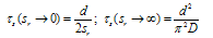
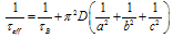
- Consider a p-type semiconductor with light incident on the sample. The light may be steady state or transient. The continuity equation for uniform ehp generation and zero surface recombination is [12,13]
 | (20) |
 | (21) |
 | (22) |
 | (23) |
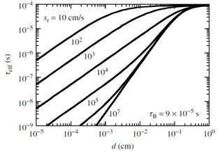 | Figure 6. Effective lifetime versus wafer thickness as a function of surface recombination velocity. D = 30 cm2/s |
 | (24) |
 | (25) |
|
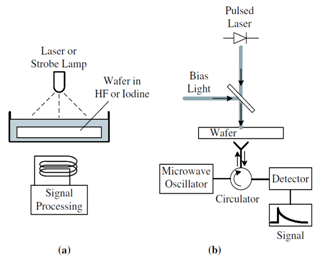 | Figure 7. PCD measurement schematic for contactless (a) rf bridge and (b) microwave reflectance measurements |
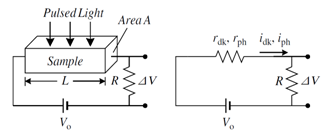 | Figure 8. Schematic diagram for contact photoconductance decay measurement |
4. Conclusions
- The microwave reflection or inductive coupling photoconductance decay technique is commonly used to measure carrier lifetime. Its key strength is the contactless nature and rapidness and major weakness is the unknown surface recombination velocity. If the sample thickness can be changed, then both the bulk lifetime and the surface recombination velocity can be extracted. The quasi-steady-state photoconductance method is a more recent method and has found wide acceptance in the design of photovoltaic devices. It measures the lifetime as a function of injection level in one step but requires large sample area (several cm2) precluding high density mapping. Surface photovoltage technique is used to detect iron in p-Si. The most common electrical recombination lifetime method is the open-circuit voltage decay method. Measured τr or Ln mean little for thin layers, e.g., epitaxial layers on highly doped substrates, denuded zones on heavily precipitated substrates, or SOI films. Such layers are best characterized through generation lifetime characterization [16] which is commonly determined with the pulsed MOS capacitor. The Zerbst plot implementation is the most common, but the current versus inverse capacitance is easier to interpret because the doping density of the sample need not be known. Since τg is measured in the space-charge region of a reverse-biased device, it lends itself easily for the characterization of thin layers. Since the scr width can be varied by an applied voltage, it is possible to generate a τg depth profile, that is difficult to do with τr measurements, because the measurement depth for τr and Ln measurements is the minority carrier diffusion length.
ACKNOWLEDGEMENTS
- Authors of this paper would like to thank the Department of EEE, BUET, Dhaka-1000, Bangladesh, for its various supports during the preparation of this manuscript.