-
Paper Information
- Next Paper
- Paper Submission
-
Journal Information
- About This Journal
- Editorial Board
- Current Issue
- Archive
- Author Guidelines
- Contact Us
International Journal of Optoelectronic Engineering
2012; 2(2): 1-4
doi: 10.5923/j.ijoe.20120202.01
Physical Properties of ZnxCd1-xS Nanocrytalline Layers Synthesized by Solution Growth Method
 Abstract
 Reference
 Full-Text PDF
 Full-Text HTML
K. Nagamani 1, M.V. Reddy 2, Y. Lingappa 1, K. T. Ramakrishna Reddy 2, R. W. Miles 3
1Department Chemistry, Sri Venkateswara University, Tirupati, 517502, India
2Department of Physics, Sri Venkateswara University, Tirupati, 517502, India
3School of CEIS, Northumbria University, Newcastle, NE18ST, U.K
Correspondence to: K. Nagamani , Department Chemistry, Sri Venkateswara University, Tirupati, 517502, India.
| Email: |  |
Copyright © 2012 Scientific & Academic Publishing. All Rights Reserved.
In recent years, zinc cadmium sulphide (ZnxCd1-xS) alloy compounds have paid much attention in the fields of opto-electronics, particularly in photovoltaic devices because of its tunable energy gap and the lattice parameters. The energy band gap of ZnxCd1-xS is controlled by the change of Zn-composition in order to suit the material properties with that of absorber material in solar cells. In this paper, we report on the effect of Zn-composition on physical properties of ZnxCd1-xS thin films deposited on corning glass substrates by solution growth method. The layers were prepared for different ‘x’ values that vary in the range, 0 – 1.0 at. %. The as-grown layers were characterized using EDAX, XRD, SEM, and UV-Vis-NIR spectrophotometers. All the layers showed a strong (002) plane as the preferred orientation that exhibited the hexagonal crystal structure. The composition of the layers agrees approximately with that of the elements in the solution. The films showed an average optical transmittance of 72 % at a zinc composition of 0.75 with a band gap of 3.88 eV.
Keywords: ZnxCd1-xS films, Solution growth, Composition, Structure, Optical properties
Article Outline
1. Introduction
- In recent years, semiconductor materials have received renewed interest due to their novel properties. Among a variety of semiconductor materials, the wide-band gap binary II–VI compounds and their alloys have been investigated most extensively for their potential application in different fields such as opto-electronic devices[1], nonlinear optical and luminescence devices[2,3] because of the quantum-size effect[4,5], especially their tunable optical property [6,7]. Alloying of semiconductors is one of the simplest techniques used for tailoring the energy band gap, lattice parameter, electronic and optical properties[8]. Generally in alloys, the lattice parameter varies linearly with composition and follows the Vegard’s law. In some of the II–VI alloy materials, the energy gap variation with composition is not very smooth and they show slight bowing. In a wider region however, the band gap tailoring also obeys Vegard’s law[9]. Currently, the ternary II–VI semiconductor materials have attracted more interest than the binary II–VI compounds due to their better physical properties compared to other materials, especially their tunable optical properties which could be controlled by their constituent mole-fraction, particle size, and morphology. Among the different ternary II-VI semiconductors, ZnxCd1-xS has been widely used as a wide band gap material in heterojunction solar cells[10–12] and in photoconductive devices[13]. Moreover, in CuGaSe2 heterojunction solar cells, the use of ZnxCd1-xS led to an increase of photocurrent by minimising the electron affinity mismatch between the two semiconductos. Further, ZnxCd1-xS can also be used as a window material in the fabrication of p–n junction solar cells without lattice mismatch in the devices based on quaternary materials like CuInxGa1-xSe2 or CuIn(SzSe1-z)2[14]. Although ZnxCd1-xS layers have been synthesized by different techniques[10-14], solution growth method is a simple technique to grow thin films that are uniform and free from pinholes. This method is also known as chemical bath deposition and normally performed under the atmospheric pressure at ambient temperatures. In this paper, we report on the effect of alloying on the physical properties of ZnxCd1-xS thin films deposited on corning glass substrates by solution growth method.
2. Experimental Details
- Thin films of ZnxCd1-xS were prepared by simple and economic process, chemical bath deposition method for different Zn-composition that varied in the range, 0 – 1.0 at. %. The deposition bath contained 0.1M aqueous solutions of zinc acetate, cadmium acetate and thiourea, taken as precursors for Zn, Cd and S respectively. The mixture was stirred well using a controllable magnetic stirrer. Ultrasonically cleaned Corning 7059 glass substrates were vertically dipped in the deposition bath while stirring of the solution continues. The deposition was carried out at a bath temperature of 70℃ for a reaction time of 30 min. A thin layer with bright yellow color was formed on the surface of the substrates. These substrates were removed from the beaker washed with de-ionized water to remove the loosely adherent powder precipitates in the solution during deposition and then dried in hot air. The as-grown layers were characterized by studying the structural, optical and electrical properties. The crystallinity of the films was measured using a Siefert X-ray diffractometer with Cu-Kα radiation source (λ=1.54 Å). The morphological properties of the films were evaluated using the Hitachi scanning electron microscope (SEM). The optical transmittance measurements were performed using a Hitachi UV-Vis-NIR spectrophotometer.
3. Results and Discussion
- Pure CdS films appeared bright yellow in color and became pale yellow as more Zn replaces Cd in the layers. All the layer were uniform and strongly adherent to the substrate surface.
3.1. Film Composition
- Fig.1. shows the chemical composition of ZnCdS films evaluated using EDAX. The EDAX spectra indicated well defined peaks corresponding to Zn, Cd and S in addition to O. All the grown films showed Se deficiency irrespective of the Zn-composition. The presence of oxygen in the layers was due to the surface contamination because the films were prepared using a non vacuum technique, CBD and/or also due to the incomplete reaction of the bath mixtures.
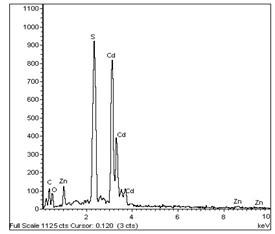 | Figure 1. EDAX spectrum of Zn0.25Cd0.75S film |
3.2. Structural Properties
- The crystallographic studies made using X-ray diffraction analysis clearly indicated the effect of alloying on the crystalline quality of the grown layers. The X-ray diffraction spectra of ZnxCd1-xS films with three different ‘Zn’ composition, x = 0.25, 0.5 and 0.75 are shown in Fig. 2. The X-ray diffraction patterns of the layers showed the same preferential orientation without secondary phases in the investigated composition range. The X-ray diffraction patterns mainly exhibited peaks related the (002), (101), (110) and (112) reflections of the hexagonal structure. All the layers exhibited the (002) crystal plane as the preferential orientation and its intensity increases with the increase of zinc content in the layers. As the samples are originated from hexagonal structure, no phase transition occurred with the increase of Zn/Cd ratio in the films. The position of diffraction peaks shifted to higher 2θ values with the increase of Zn-content. The X-ray diffraction results are in good agreement with the reported results[15,16].
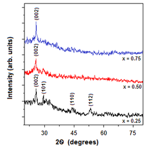 | Figure 2. X-ray diffraction profiles of ZnxCd1-xS films |
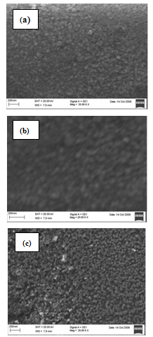 | Figure 3. SEM micrographs of ZnxCd1-xS films; (a) x=0.25, (b) x=0.5 and (c) x=0.75 |
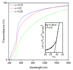 | Figure 4. Transmittance versus wavelength plot of ZnxCd1-xS films (inset shows (αhυ)2 versus hυ plot for Zn0.75Cd0.25S film) |
5. Conclusions
- Thin films of ZnxCd1-xS have been successfully prepared by simple and economic process, chemical bath method with different ‘Zn’ compositions that varied in the range, 0 – 1 at % at a constant bath temperature of 70℃ for a reaction time of 30 min. All the layers showed a strong (002) plane as the preferred orientation that exhibited the hexagonal crystal structure. The variation of lattice constants with Zn- composition showed linear behavior. The evaluated average grain size was found to vary from 45 nm to 76 nm. SEM micrographs revealed the grains on the film surface were more compact and have dense structure. The films showed an average optical transmittance of 72 % at a zinc composition of 0.75 and exhibited a band gap of 3.88 eV. By suitably controlling the Zn-composition in the layers, the ZnxCd1-xS films may have minimum lattice mismatch that that of pure CdS with some of the absorber layers, particularly with chalcopyrite compounds.
ACKNOWLEDGEMENTS
- The authors would like to thank the University Grants Commission (UGC), New Delhi for the financial support.