-
Paper Information
- Previous Paper
- Paper Submission
-
Journal Information
- About This Journal
- Editorial Board
- Current Issue
- Archive
- Author Guidelines
- Contact Us
International Journal of Optoelectronic Engineering
p-ISSN: 2167-7301 e-ISSN: 2167-731X
2011; 1(1): 7-11
doi: 10.5923/j.ijoe.20110101.02
Nonlinear Material Based All-Optical Parallel Subtraction Scheme: an Implementation
 Abstract
 Reference
 Full-Text PDF
 Full-Text HTML
Samir Sahu 1, Radha Raman Pal 1, Shantanu Dhar 2
1Department of Physics and Technophysics, Vidyasagar University, Midnapore, 721102, India
2Department of Physics, Jhargram Raj College, Jhargram, 721507, India
Correspondence to: Samir Sahu , Department of Physics and Technophysics, Vidyasagar University, Midnapore, 721102, India.
| Email: |  |
Copyright © 2012 Scientific & Academic Publishing. All Rights Reserved.
Non-linear material based all-optical switching mechanism is utilized here to implement the all-optical parallel subtraction scheme. Optical tree architectures here convert analog optical signal to the corresponding digital one. A two bit all-optical binary parallel subtractor has been proposed and which may be elevated to a higher bit parallel subtractor in course using all-optical half-subtractor and a full-subtractor. These are constructed by a composite slab of linear medium (LM) and non-linear medium (NLM) and it is the building block of our proposed subtructor circuit. These circuits are all-optical and fully parallel in nature. It can also gear up to the highest ability of optical performance in high-speed all-optical computing system.
Keywords: Nonlinear Material, All-Optical Switch, Optical Tree Architecture, All-Optical Logic Gate, All-Optical Parallel Subtractor
Cite this paper: Samir Sahu , Radha Raman Pal , Shantanu Dhar , "Nonlinear Material Based All-Optical Parallel Subtraction Scheme: an Implementation", International Journal of Optoelectronic Engineering, Vol. 1 No. 1, 2011, pp. 7-11. doi: 10.5923/j.ijoe.20110101.02.
Article Outline
1. Introduction
- As our modern life is becoming faster day by day, in the current decade, scientific and engineering problems are specially confined in a particular area to attain the reliable, faithful and high speed performances in computation[1-3,5] and communication[4,6]. Unfortunately, the VLSI technology, so far is being used, cannot beat this challenge. Electrons have a limited speed. So, this technology is already in a saturated state from both the aspects – size and speed. Moreover, our venture for the advancement of this technology creates new problems like hot carriers, electromagnetic interference, short channel effects etc. These factors endanger the device reliability.Presently, in fewer fields, electronic devices are replaced by electro-optical (OE) devices[6,11]. This technology tem- porarily overcomes some physical problems. But the previous limitations still exist as electronic parts are still there in those hybrid components.In the above circumstances, there is a way-out to replace the traditional circuits with all-optical ones[2-3,7,15-17]. Photonics is the future of technology. In the last few years, light, as signal carrier, has already established its validity in various all-optical operations[1-3,5-7,9,11,15-23]. Among many other techniques, non linear material (NLM) has been established its validity as optical switching devices[1-3,5,9]. All-optical signal processing technologies by non-linear material based directional switch are considered as a possible long-term route in the evolution of current telecommunication network and ultra high-speed signal processing[10-17]. The all optical implementation of various subtraction schemes[5] have been studied by taking the complement of the subtrahend and adding it to the minuend. The schemes for optical implementation of subtractors using Semiconductor Optical Amplifier (SOA)[6] and electro-optic- modulators (EOM)[11] have been attempted. The paper presents a scheme for the implementation of all optical Parallel Subtractor (PS)[10] by Half Subtractor (HS) and Full Subtractor (FS)[15] with logic circuits in direct manner [8,10], as done with paper and pencil, by nonlinear optical material based switching mechanism, in such a way that will obey the truth table[8,10,15]. By this method, each subtrahend bit of the number is subtracted from its corresponding significant minuend bit to get DIFFERENCE bit including the case of BORROW bit, as in conventional electronics. Our proposed circuits are very much reliable because they follow the basic principle of subtraction operation. An ALU of dream goal, an optical computer, can be implemented including this scheme.
2. All-optical Switching Behaviour of Nonlinear Material and its Use as All-optical Gates
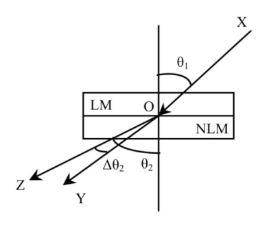
- The phenomenon photorefractivity[13-17] of some non- linear optical material is used in nonlinear all-optical intensity switching mechanism. The photorefractive effect, where the refractive index changes induced by a light field when the crystal is subjected to intense laser radiation, defocusing and scattering of the light, is observed, as a result of an inhomogeneous change in the refractive index. It is also found that these changes still prevail even after the light is switched off, but it could be erased by strong, uniform illumination [14].The refractive index of some nonlinear materials (NLM) such as carbon disulfide, pure silica, potassium dihydrophosphate (KDP), (KH2PO4) crystal etc. varies linearly with the intensity of the light incident on it. The refractive index (n) of such isotropic dielectric non-crystalline media can be put into an equation as in (1).
 | (1) |
 | Figure 1. Intensity switching of optical nonlinear material |
2.1. All Optical NOT Gate
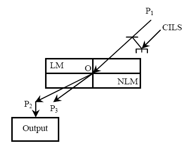
- To implement an all optical NOT gate using non-linear material a constant intensity pulse laser source (CILS) is used as shown in Figure 2. It is also called probe beam. Here P1 is taken as input beam. A detector is placed at P2 will detect the output beam after refraction. If P1 is absent, the light will follow a path OP2 and will be detected by the detector due to presence of CILS. But if P1 is present, after refraction, the light will follow a path other than OP2, may be OP3, and the detector will not detect any light signal. Thus the system acts as optical NOT gate.
 | Figure 2. All-optical NOT gate |
2.2. All-optical Ex-OR Gate
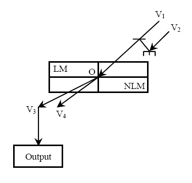
- The two inputs all-optical XOR gate using NLM is shown in Figure 3. Here V1 and V2 are two input channels. A detector is placed at V3 gives the output. When only one input channel carries light signal, the light beam after refraction will detect by the detector at V3, unless not.
 | Figure 3. All-optical EX-OR gate |
2.3. All Optical AND Gate
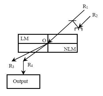
- The two inputs all-optical AND gate using NLM is shown in Figure 4. Here R1 and R2 are two input channels. A detector is placed at R4 gives the output. Now when both the channels carry light signal, the light beam after refraction one can get light at the detector (situated at R4), unless not.
 | Figure 4. All-optical two-input AND gate |
 | Figure 5. All optical three-input one-or-all circuit |
2.4. All Optical Three-input One-or-all Circuit
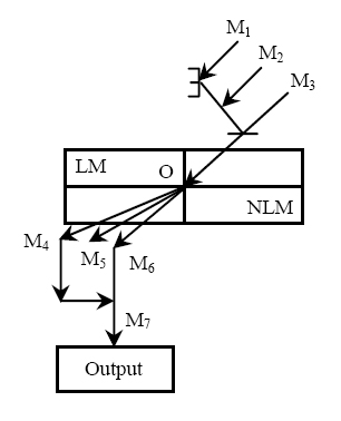
- The all-optical three-input one-or-all circuit using NLM is shown in Figure 5. Here M1, M2 and M3 are three input channels. A detector is placed at M7 gives the output. Now when any one of the input channels carries light signal, the light beam after refraction will detected by the detector at M7 and there will be light at M7 if all the inputs have light also The output remains dark for all other combinations of input states.
2.5. All Optical Three-input Two-or-all Circuit
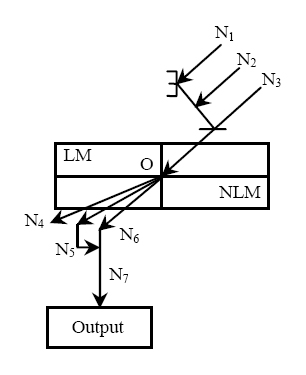
- The all-optical three-input two-or-all circuit using NLM is described in Figure 6. Here N1, N2 and N3 are three input channels. A detector is placed at N7 gives the output. Now when any two or all of the input channels carry light signal, the light beam after refraction will detected by the detector at M7, unless not.
 | Figure 6. All optical three-input two-or-all circuit |
 | Figure 7. All-optical parallel subtraction schem using NLM as switch |
3. All-Optical Parallel Subtractor
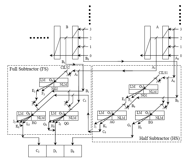
- We design an all-optical binary subtraction scheme capable of subtraction between two multibit data in parallel. The system is shown in the Figure 7. Tree architectures[1,5,9] A and B are used to convert a decimal value into its respective binary value, A1A0 and B1B0 respectively. Here B1B0 is to be subtracted from A1A0. One 1-bit full subtractor[15] and one 1-bit half subtractor[15] system are combined to obtain a general all optical parallel subtraction. For half subtractor system[15] A0 and B0 are the two inputs. The outputs are taken from D0 (DIFFERENCE) and C0 (BORROW). The all optical half subtractor is constructed by three all optical logic gates. NG1, EG and AG are the optical NOT gate, two-input EX-OR gate and two-input AND gate respectively. The truth table of an all-optical half subtractor is given in Table 2[8,10,15]. For full subtractor[15], the inputs are A1, B1 and C1 (= C0 BORROW from previous half subtractor). The outputs are from D1 (DIFFERENCE) and C2 (BORROW). The all optical full subtractor is implemented with an all optical NOT gate (NG2), a three-input one_or_all circuit (QG) and a three-input two_or_all circuit (RG). The truth table of an all-optical full subtractor is set in Table 3 [8,10,15]. The final output result is C2D1D0. This is the binary output of (A1A0 – B1B0).Let us consider an example for subtracting 3 from 2. We take A = 2 and B = 3. The binary equivalent of A = 2 is A1A0 = 10 and the binary equivalent of B = 3 is B1B0 = 11.
| |||||||||||||||||||||||||||
| |||||||||||||||||||||||||||||||||||||||||||||||||||||
4. Conclusions
- Our proposed circuits are very much reliable because they follow the basic principle of subtraction operation. The light signals that are severally used, bended and the feedback light signals from the outputs are made by mirrors and beam splitters to make the circuits simple. As the circuit is purely all-optical in nature and very simple, one can obtain the speed of operation far more than THz limit[2,3,12-24]. This subtraction scheme should be the first step on our dream way to all-optical Arithmetic Unit. The entire scheme should perform properly using suitable nonlinear material[2,3, 12-17,24]. Essentially inputs should be chosen properly for proper function of the system.
ACKNOWLEDGEMENTS
- The authors want to acknowledge Professor Sourangshu Mukhopadhyay of the for his valuable suggestions.
References
| [1] | K. R. Choudhury and S. Mukhopadhyay, “A new method of binary addition scheme with massive use of non-linear material based system,” Chinese Optics Letters, vol. 1, no. 4, pp. 132, 2003 |
| [2] | S. Dhar and S. Sahu, “All-optical implementation of S-R, clocked S-R and D flip-flops using nonlinear material,” Opt. Eng. 47(6), 065401-1-6, 2008 |
| [3] | S. Sahu and S. Dhar, “Implementation of clocked J-K, T and J-K Master Slave flip-flops with nonlinear material in All-optical Domain,” Opt. Eng. 48(7), 075401-1-7, 2009 |
| [4] | S. Mironov. V. Lozhkarev, V. Ginzburg and E. Khazanov, “High-efficiency second-hermonic generation of superintense ultrashort laser pulses,” Applied Optics. 48, 2051-2057, 2009 |
| [5] | K. R. Choudhury and S. Mukhopadhyay, “Binary optical arithmetic operation scheme with tree architecture by proper accommodation of optical nonlinear materials,” Optical Engineering, vol. 43, no. 1, pp. 132, 2004 |
| [6] | Li Pei-Li, Huang De-Xiu, Zhang Xin-Liang and Wang Yang, “Single-SOA-Based Ultrahigh-Speed All-Optical Half Subtracter with PolSK Modulated Signals,” Chinese Physics Letters, vol. 25, no. 5, pp. 1705, 2008 |
| [7] | S. K. Garai and S. Mukhopadhyay, “All-optical frequency encoded binary half subtractor using periodically poled lithium niobate waveguide and reflecting semiconductor optical amplifier,” Optics and Photonics Letters, vol. 3, no. 1, pp. 15, 1010 |
| [8] | M. Morris Mano, Digital Logic and Computer Design (Prentice-Hall of India Private Limited, New Delhi, 2000) |
| [9] | S. Mukhopadhyay, “An optical conversion system: from binary to decimal and decimal to binary,” Optics Communications, vol. 76, pp. 309, 1990 |
| [10] | R. P. Jain, Modern Digital Electronics, 3rd ed., Tata MaGraw-Hill India, New Delhi. India: 2007 |
| [11] | A. Sinha, H. Bhowmik, P. Kuila, and S. Mukhopadhyay, “A new method of controlling the power of a gaussion optical pulse through electro-optic modulator and non-linear wave guide for generation of soliton,” Optical Engineering, vol. 44, no. 6, pp. 065003, 2005 |
| [12] | D Samanta, S. Mukhopadhyay, “A method of maintaining the intensity level of a polarization encoded light signal,” Journal of Physical Science. 11, 87-91, 2007 |
| [13] | S. D. Smith, I. Janossy, H. A. Mackenzi, J.G. H. Mathew, J. J. E. Reid, M. R. Taghizadeh, F. A. P. Tooley and A. C. Walker, “Nonlinear optical circuit elements, logic gates for optical computers: the first digital optical circuits,” Optical Engineering, vol. 24, no. 4, pp. 569-573, 1985 |
| [14] | D. Arivouli, “Fundamentals of optical nonlinear materials,” Pramana. 57(5-6) 871-883, 2001 |
| [15] | S. Sahu, R. R. Pal and S. Dhar, “A Novel Method of Implementing Nonlinear Material Based All-Optical Binary Half Subtractor and Full Subtractor System,” J. of Electron Devices. 10, 493-498, 2011 |
| [16] | S. Sahu, R. R. Pal and S. Dhar, “TeraHertz All-Optical Binary Register using D flip-flop with Non-linear Material: A Proposal” J. of Electron Devices. 11, 588-595, 2011 |
| [17] | S. Sahu, R. R. Pal and S. Dhar, “All-Optical Binary Counter by using T flip-flop: An Implementation” International Journal of Engineering, Science and Technology. 3(10), 7799-7807, 2011 |
| [18] | A. Yang, Z. Liu, B. Wang, Y. Zhang and S. Liu, “Optical stream-cipher-like system for image encryption based on Michelson interferometer,” Opt. Exp. 19(3), 2634-2642, 2011 |
| [19] | E. Lazzeri, G. Berrettini, G. Meloni, A. Bogoni and L. Poti, “All-Optical-Bits Shift Register Exploiting a Ring Buffer Based on Semiconductor Optical Amplifier,” Phot. Tech. Lett. IEEE. 23(1), 45-47, 2011 |
| [20] | G. Berrettini, L. Potì and A. Bogoni, “Optical Dynamic RAM for All-Optical Digital Processing,” Photonics Technology Letters, IEEE. 23(11), 685-687, 2011 |
| [21] | N. Pahari and S. Mukhopadhyay, “An all optical R-S flip-flop by optical non-linear material,” J. of Opts. 34 (3), 108114, 2005 |
| [22] | A. K. Datta and S. Munshi, “Optical implementation of flip-flops using single-LCD panel,” Opt. & Laser Tech. 39(9), 2321-2329, 2007 |
| [23] | T. Chattopadhyay, "All-optical clocked delay flip-flop using a single terahertz optical asymmetric demultiplexer-based switch: a theoretical study," Appl. Opt. 49, 5226-5235, 2010 |
| [24] | M. Choi, S. H. Lee, Y. Kim, S. B. Kang, J. Shin, M. H. Kwak, K.Y. Kang, Y. H. Lee, N. Park and B. Min, “A terahertz metamaterial with unnaturally high refractive index,” Nature. 470, 369-373, 2011 |