-
Paper Information
- Next Paper
- Paper Submission
-
Journal Information
- About This Journal
- Editorial Board
- Current Issue
- Archive
- Author Guidelines
- Contact Us
International Journal of Optoelectronic Engineering
p-ISSN: 2167-7301 e-ISSN: 2167-731X
2011; 1(1): 1-6
doi: 10.5923/j.ijoe.20110101.01
Speed Performance Degradation of Electrooptic Modulator Devices by Neutrons Irradiations at High Temperature Effects
 Abstract
 Reference
 Full-Text PDF
 Full-Text HTML
Ahmed Nabih Zaki Rashed
Electronics and Electrical Communication Engineering Department, Faculty of Electronic Engineering, Menouf, Menoufia University, 32951, Egypt
Correspondence to: Ahmed Nabih Zaki Rashed , Electronics and Electrical Communication Engineering Department, Faculty of Electronic Engineering, Menouf, Menoufia University, 32951, Egypt.
| Email: |  |
Copyright © 2012 Scientific & Academic Publishing. All Rights Reserved.
In the present paper, we have deeply investigated the transmission efficiency degradation of electrooptic modulator devices in thermal irradiated hard environments over wide range of the operating parameters. It is well known that the radiation-induced electrooptic modulator defects can modify the initial doping concentrations, creating generation-recombination centres and introducing trapping of carriers. Additionally, rate of the lattice defects is thermally activated and reduces for increasing irradiation temperature as a result of annealing of the damage. Both the ambient temperature and the irradiation dose possess sever effects on the electro-optical characteristics and consequently the performance characteristics of electroptic modulator devices. As well as we have deeply developed the modelling basics of electrooptic modulator devices, which may be used to analyzed the modulator quantum efficiency, dark current, modulating voltage, modulating frequency, 3-dB bandwidth, transmitted signal bandwidth, modulator quality factor, modulator sensitivity, modulator sensitivity bandwidth product, switching voltage, modulator device performance index, operating switching time and speed response of these irradiated electrooptic modulator devices after different irradiation fluences.
Keywords: Radiation Damage, Switching Time, Quality Factor, Neutrons Irradiations, Switching Voltage
Cite this paper: Ahmed Nabih Zaki Rashed , "Speed Performance Degradation of Electrooptic Modulator Devices by Neutrons Irradiations at High Temperature Effects", International Journal of Optoelectronic Engineering, Vol. 1 No. 1, 2011, pp. 1-6. doi: 10.5923/j.ijoe.20110101.01.
Article Outline
1. Introduction
- Modulators and optical fibers have previously been irradiated with neutrons within thermal effects[1]. The modulators were unaffected in terms of their reflectance. The leakage current, which does not affect their performance, increased from 5 nA to 100 nA. Of the fibers that were irradiated, pure silica core fibers were found to be more radiation hard than Ge-doped fiber. This result was expected as the induced losses in the fibres are believed to be related to the defects introduced by dopants such as germanium. The dose rates used were around two orders of magnitude greater than those expected at high irradiation doses. Therefore, taking fibre annealing into consideration, the pure silica core fibres are sufficiently resistant ton on-ionising radiation damage for high irradiation fluence use[2]. The modulators are based on III-V semiconductor electro-absorptive multi quantum well structures grown between asymmetric Fabry-Perot mirrors. The electro-absorption in the devices tested was tuned to obtain a maximum modulation depth at a wavelength of 1.54 μm. Reflectivity of the device is modula-ted by varying the applied electric field across the quantum wells. The devices tested here were configured as a linear array of 8 channels, with active modulator quantum well areas of 30 μm diameter at 125 μm pitch.Optical communication systems are becoming the norm in communication applications. These systems have many advantages over electrical communication systems: low weight and size, mechanical simplicity, high data rates, high sensitivity and multiplexing capabilities and resistance to electromagnetic interference (EMI). Those advantages make this technology very attractive. They are preferable in radiation environments such as space borne systems, medical applications and nuclear facilities[2]. Their applications involve communication, remote sensing and monitoring. Whereas most efforts are oriented towards assessing the applicability of optical and photonic components for data transmission, far less attention is paid to the use of these components as sensors. In radiation environments, the optical sensors might be an attractive alternative to conventional measurement techniques[3]. Other applications include fiber-optic time-resolved laser-induced fluorescence for uranium and nitrate sensing, fiber optic Raman spectroscopy for waste tank monitoring and fiber dosimetry with scintillating optical fibers or induced absorption in optical fibers. Fiber-optics are envisaged for the construction of image guides or fiberscope-type viewing systems as an alternative to very radiation sensitive charge coupled devices (CCD) cameras to achieve visual inspection in nuclear power plants. There is a great need for optical communication for space flight usage for remote sensing and in optical communications applications. For remote sensing applications the fiber laser provides: an ultra stable compact source for laser vibrometry. Also the sensing application of photonic technologies to space including velocity sensors for gyroscope systems. The combination of fiber optic gyroscope and accelerometer measurements determine the instantaneous position and trajectory vehicle[4].The modulators were reverse biased at -7 Volt during the irradiation in order to monitor any annealing of the leakage current which was measured and recorded every 60 seconds. Radiation damage caused the leakage current in most of the channels to increase to about 100 nA. In comparison, the photocurrent generated by the modulator under normal operating conditions is in the range of 10 to 100 μA[4]. In most cases the leakage current was fully annealed in the three days after irradiation. The channels which had not annealed in this time were remeasured later and the leakage current was found to have decreased to preirradiation levels. The increases in the leakage current are thought to be associated with radiation induced charging of the polyimide layer used to isolate neighbouring multi quantum well structures[5]. This hypothesis may be confirmed by future tests on similar devices without polyimide.In the present study, Measurements of the reflectivity of the electrooptic modulators at different bias voltages were made before and after irradiation showing no significant change. The modulators were irradiated under bias with the dark current in the devices continuously monitored during different doses after the irradiation. Increases in the dark current were observed due to radiation damage though the devices were fully annealed after irradiation fluences. Our results have suggested that the electrooptic modulator devices are sufficiently resistant to ionizing radiation though further tests are required. The transmission efficiency, sensitivity bandwidth product and device performance index were monitored throughout the irradiation for sufficient period time after irradiation.
2. Modeling Analysis
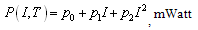
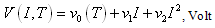
- The point defects result in the introduction of allowed energy states within the forbidden gap of the semiconductor. This energy states lead to the following: (a) Carrier removal is the majority carrier density is reduced by the radiation fluence, (b) Mobility degradation is the mobility was found to decrease with increasing the radiation fluence[6], (c) Conductivity modulation since the carrier concentration and mobility both decrease with radiation, then the conductivity will also decrease, and (d) Minority carriers lifetime can be defined as the degradation rate in minority carrier lifetime and can be expressed as:
 | (1) |
 | (2) |
 | (3) |
 | (4) |
 | (5) |
 | (6) |
 | (7) |
 | (8) |
 | (9) |
 | (10) |
 | (11) |
 | (12) |
 | (13) |
 | (14) |
 | (15) |
 | (16) |
 | (17) |
 | (18) |
 | (19) |
 | (20) |
 | (21) |
 | (22) |
 | (23) |
 | (24) |
 | (25) |
 | (26) |
 | (27) |
 | (28) |
 | (29) |
3. Simulation Results and Performance Analysis
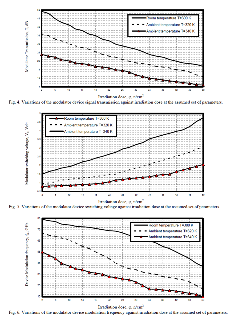
- We have investigated the transmission efficiency degradation of electrooptic modulator devices in thermal irradiated hard environments under the set of the wide range of the affecting and operating parameters are listed as follows: Confinement factor Г = 0.8–0.95, Specific resistivity ρ = 2.66x10⁻⁶ Ω.μm, Electro-optic coefficient r33 = 300 pm/Volt, Relative refractive index difference Δne = 0.01, Bias voltage VB = 2 Volt, Modulator thickness d=0.02 μm, Dark current id = 0.01 μA, Switching time Ts = 0.8 msec, Speed of light c = 3 x1010 cm/sec, Modulator length Lm = 0.2 μm, Modulator width W = 0.1μm, Room temperature T0 = 300 K, Ambient temperature T = 300–340 K, Operating signal wavelength λ= 1.55 μm, Electron charge q = 1.6x10⁻¹⁹ C, Quantum efficiency η= 90%, applied drive current I = 2 mA, irradiation fluence or dose φ = 2x10¹⁴–50x1014 n/cm2. Based on the model equations analysis, assumed set of the operating parameters as listed previously, and based on the series of the Figs. (1–7), the following facts are assured:
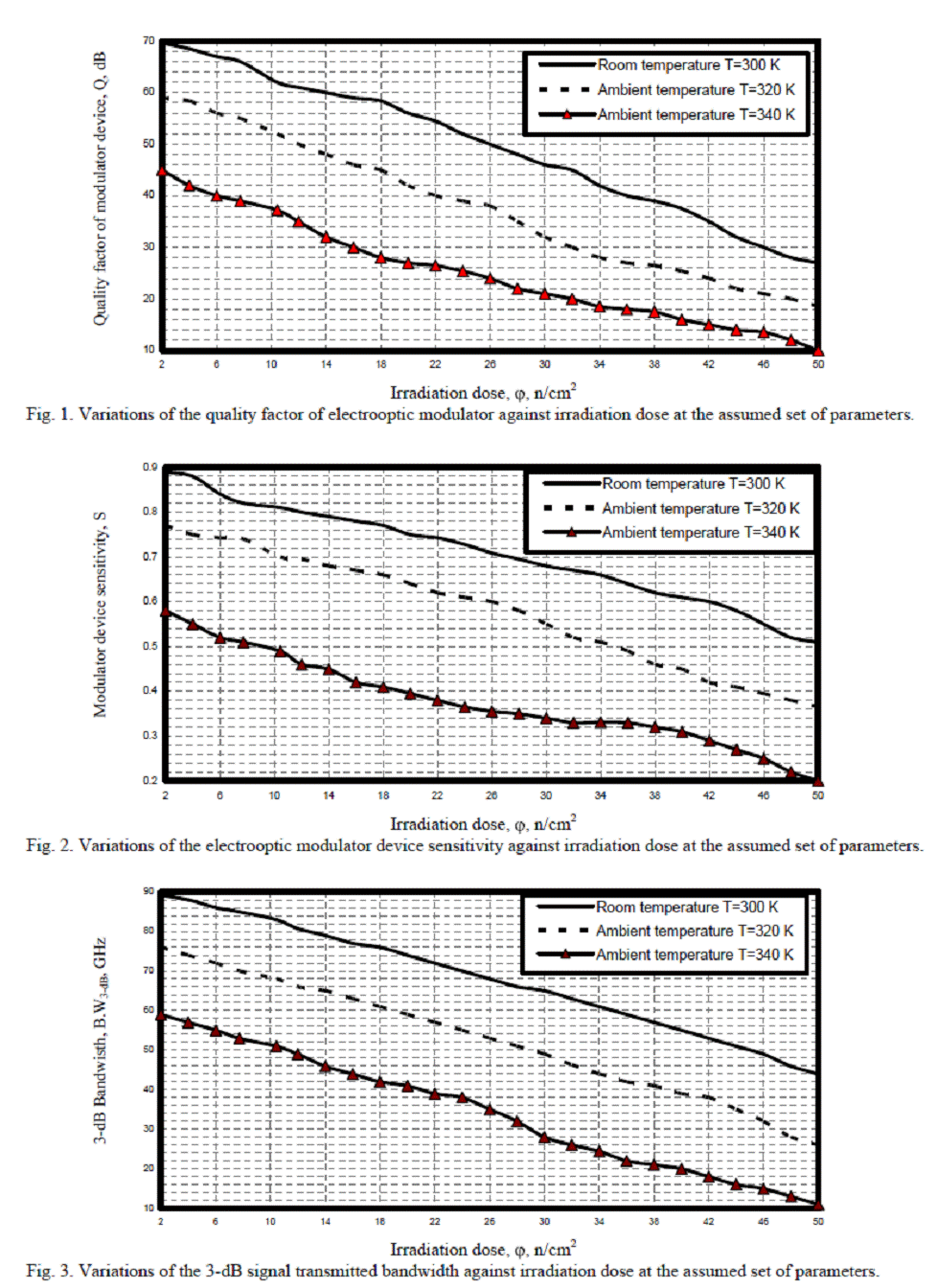 | Figure 1. Variations of the quality facter of electrooptic modulator against irradiation dose at the assumed set of parameters |
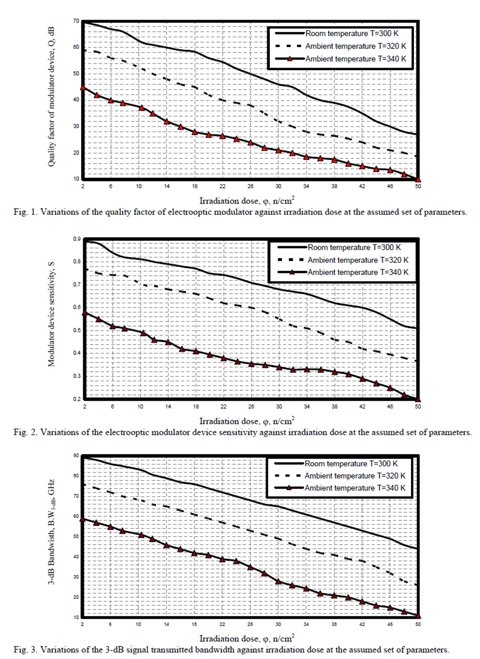 | Figure 2. Variations of the electrooptic modulator device sensitivity against irradiation dose at the assumed set of parameters |
 | Figure 3. Variations of 3-dB signal transmitted bandwidth against irradiation dose at the assumed set of parameters |
 | Figure 4. Variations of modulator device signal transmission against irradiation dose at the assumed set of parameters |
 | Figure 5. Variations of modulator device switching voltage against irradiation dose at the assumed set of parameters |
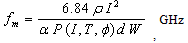
 | Figure 6. Variations of modulator device modulation frequency against irradiation dose at the assumed set of parameters |
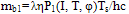
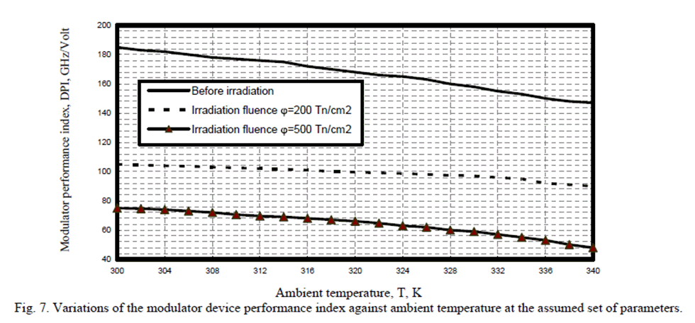 | Figure 7. Variations of modulator device performance index against ambient temperature at the assumed set of parameters |
4. Conclusions
- In a summary, we have been deeply investigated the speed performance degradation of electrooptic modulator devices under high temperature variations and different irradiation doses environment. It is theoretically found that the increase of both irradiation doses and ambient temperature variations, the decreased modulator device quality factor, modulator device sensitivity, transmitted signal bandwidth, modulator transmission, device modulation frequency, and the modulator device performance index. It is also evident that the increased ambient temperature and irradiation doses, this leads to the increased modulator switching or driving voltage. Thus the increased thermal irradiated fields has the great harmful effects on the modulator speed performance and transmission efficiency. To the best of our knowledge, high thermal irradiated environments study on the highest driving voltage and operating device parameters of electrooptic modulators has been performed particularly operating at 1.55 mm wavelength.