Minami Takato, Ken Saito, Fumio Uchikoba
Department of Precision Machinery Engineering, Nihon University, Japan
Correspondence to: Minami Takato, Department of Precision Machinery Engineering, Nihon University, Japan.
| Email: |  |
Copyright © 2016 Scientific & Academic Publishing. All Rights Reserved.
This work is licensed under the Creative Commons Attribution International License (CC BY).
http://creativecommons.org/licenses/by/4.0/

Abstract
This paper proposes a fabrication process and multilayer ceramic wireless power transfer. Conventional wireless power transfers are the electromagnetic induction type and the coil is fabricated by a winding wire. In this paper, the ceramic wireless power transfer coil is proposed to form a miniature coil structure with a magnetic core. The fabrication process of the ceramic coil was based on the multilayer ceramic technology that is usually used for miniature electronic element, and the process is combined with the photolithography process. In the fabricated small structure of 5mm diameter, the embedded coil showed the high-aspect-ration pattern and low-internal resistance. Moreover, the fabricated embedded coil demonstrated the power transmitting.
Keywords:
Wireless power transfer, Multilayer ceramic coil, Photo resist film, Ferrite
Cite this paper: Minami Takato, Ken Saito, Fumio Uchikoba, Development of Multilayer Ceramic Wireless Power Transfer Fabricated by Photo Resist Film Process, International Journal of Materials Engineering , Vol. 6 No. 5, 2016, pp. 159-165. doi: 10.5923/j.ijme.20160605.04.
1. Background/ Objectives and Goals
Power supply is important factor. Many electronic devices such as communication devices have been miniaturized. The miniaturization of these electronic devices is supported by the miniaturization of all integrated components. Active circuit has been integrated and miniaturized by integrated circuits (ICs). Passive electronic elements are also integrated and miniaturized by a multilayer ceramic technology. Recently, miniature mechanical structural components such actuators and sensors are fabricated by a micro electro mechanical systems (MEMS) process (Tai Y-C., et al., 1989). On the other hand, the power supply method has been researched (Renaud, M., et al., 2007; Steyn, J. L., et al., 2009) to alternate the conventional battery. However, a lithium-ion battery is still dominant power source for the miniature electronic device because both small size and high power density are required.The lithium-ion battery is approaching the theoretical limit in the power density. In response to this problem, miniature generators have been studied as one of the candidates for exceeding the limit. For example, vibration-powered micro generators have been studied (Jones, P G., et al., 2001). However, These generators have used for the purpose of accumulating power from environment by means of the harvesting, because its power is too small as a main power source. Moreover, miniature generator that was fabricated by the MEMS process has been reported in various types such as an electrostatic type and an electromagnetic induction type. However, these generators show small output power.On the other hand, wireless power transfer is focused as power supply. An electromagnetic induction type power transfer has been used for the home electronics and IC cards. This type shows high transmission efficiency. Wireless power transfer is expected to apply in Electric Vehicle. Moreover, electromagnetic induction type is constructed by simple coil structures, it is possible to use for miniature medical equipment such as an implantable artificial heart and an endoscope microrobot (Yan, G., et al., 2007). However, it is requires the miniature power transfer system. To miniaturize the wireless power transfer system, the miniaturization of the coil structure is required. The wireless power transfer system has a transmitting coil and receiving coil. The coil structure is composed of winding wires, magnetic cores and diffraction yokes. It is difficult to miniaturize the coil structure because these elements are adopted by different technologies. The winding wire coil is difficult to miniaturize particularly. Often, the winding wire coil employs spiral patterns for the miniaturization. It can realize the low profile of the receiver coil. However, the spiral pattern requires a long length wire and a large area because it is extended to catch the divergence magnetic flux. Therefore, this structure shows high internal resistance.The fabrication technology that can form the miniature coil structure like a winding wire is the multilayer ceramic technology. It is usually used for the miniature electronic element such as a multilayer ceramic inductor. It can form the miniature three-dimensional structure coil by laminating ceramic sheets that are formed a conductor. And the magnetic core can be introduced by using magnetic ceramic material. Previously, we reported the wireless power transfer coil that was fabricated by the multilayer ceramic technology (Takato M., et al., 2014). In this paper, high internal resistance of the ceramic coil was a problem. The reason is the conventional fabrication process of the multilayer ceramic technology. The conductive paste was patterned by the screen printing process for forming the conductive pattern, and it was printed on the ceramic sheet. After drying the patterned conductor showed deformation by surface tension. The deformation of the conductive paste has possibility of electrical short circuit. By this reasons, the screen printing process is difficult to form a high-aspect-ratio pattern. Low-aspect-ratio pattern means small cross-sectional area of the conductive pattern, and it results in high internal resistance. We focus on the photolithography process that is used for the MEMS process and IC process to achieve the high-aspect-ration pattern. In the proposed method, a photoresist film is patterned the conductive pattern. The conductive paste is filled into the through- pattern of the resist film. By this process, the patterned conductor is held by the resist film.In this paper, we proposed the ceramic wireless power transfer coils fabricated by the photolithography process to achieve low-internal resistance coil. The one of the coil pattern is formed on the ceramic sheet, and another one is an embedded pattern into the ceramic sheet. Diameter of the designed coils is 5 mm. The fabricated coils are compared with the surface pattern coil, embedded pattern coil and screen printing coil about the thickness of coil pattern, internal resistance and the result of the wireless power transfer.
2. Designs and Methods
2.1. Design of Ceramic Coil
The proposed coil patterns are shown in Figure 1. The surface pattern coil is printed on the ceramic sheet. On the other hand, the embedded pattern coil is formed inside the ceramic sheet. Figure 2 shows the designed coil structure. The fabricated ceramic coil shapes the three-dimensional structure and circle coil pattern. The coil pattern is arranged along the outside diameter of the coil structure to suppress the passing magnetic flux at the magnetic material around the coil pattern. Diameter of the designed coil pattern is 5 mm. The turn number is 18 turns and the line width of the coil is 800 μm. The coil pattern of 23/24 turn and 3/4 turn are formed on a single sheet. The laminated number is 20 including the top layer. The magnetic material and conductive paste of the coil structure is made from low temperature sintering NiCuZn ferrite with the permeability of 900 and silver paste, respectively. 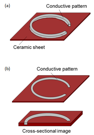 | Figure 1. Proposed coil pattern (a) surface pattern (b) embedded pattern |
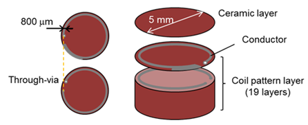 | Figure 2. Designed coil structure |
2.2. Concept and Advantage of Process
The most important characteristic of the proposed process is that the patterning photo resist film holds the conductive pattern to achieve the non-deformation pattern. Figure 3 shows the schematic illustration of the proposed patterning process. In the first step, the photo resist film is exposed for forming the designed conductive pattern. The through pattern is obtained after developing. Second step, the conductive paste is filled into the through-pattern of the resist film by a metal blade. During the dry process, the conductive paste is holding by the resist film. After that, the resist film is removed chemically. By these processes, the high-aspect-ratio conductive pattern without deformation can be formed on the sheet. It is leached the low internal resistance. Moreover, the proposed patterning process combined with the photolithography process and ceramic patterning process. It is possible to form the fine conductive pattern.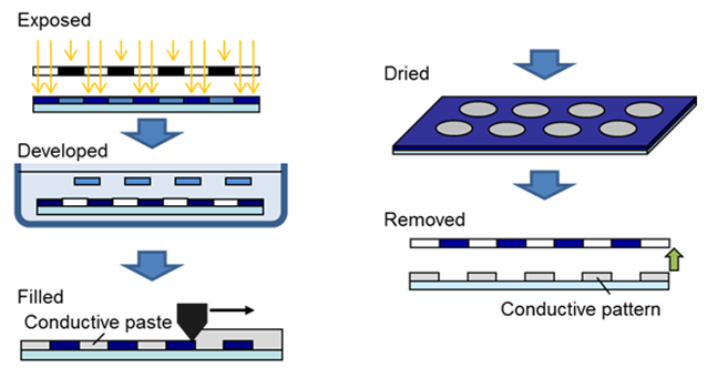 | Figure 3. Schematic illustration of the proposed patterning process |
2.3. Fabrication Process
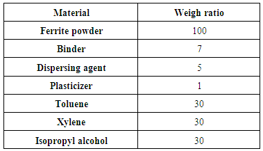
In this paper, two conductive patterns of the surface pattern and the embedded pattern were fabricated. First of all, the photo resist film was exposed to form the through-pattern. Ultraviolet light was used for exposing. The photo resist film was attached on the PET film, and the thickness was 75 μm. The exposed film was developed and rinsed. The developing solution was 1 wt% sodium carbonate at room temperature. The resist film that was formed through-pattern was achieved after dry process at room temperature.Ceramic material was required for multilayer ceramic coil. The fabricated ceramic coil had low temperature sintering NiCuZn ferrite as the magnetic material. Ferrite shows high magnetic property. Moreover, NiCuZn ferrite is possible to achieve low internal resistance electronic element by patterning silver or cupper material that shows low resistance because it can be fired at low temperature. Ferrite powder was made from NiO, CuO, ZnO, and Fe2O3, composition ratio was 8.8, 10, 32 and 49.2, respectively. Ferrite slurry was fabricated by mixing the ferrite powder, dispersing agent, plasticizer, organic materials and binder. Composite weight ratio of ferrite slurry is shown in table 1. Fabricated ferrite slurry was used for the ceramic sheet and the covered ceramic.Table 1. Composite weight ratio of ferrite slurry
 |
| |
|
In the surface pattern, patterned resist film covered on the ceramic sheet that was formed through-hole pattern to connect lower layers. The covered ceramic sheet was filled the silver paste into the through-pattern of the resist film and through-hole of the ceramic sheet. After the drying process, the resist film was removed by a tetra methyl ammonium hydroxide (TMAH) solution. The temperature of TMAH solution was room temperature. Then, the coil pattern on the ceramic sheet was achieved. Figure 4 shows schematic illustration of the fabrication process for the surface pattern.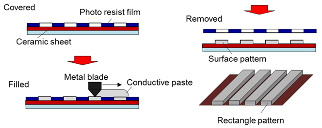 | Figure 4. Schematic illustration of the fabrication process for the surface pattern |
To achieve the embedded pattern, the developed resist film was filled the silver paste by the metal blade. The resist film was removed, and the silver pattern was formed on the PET film. The patterned conductor was covered by the ferrite slurry. At this time, the gap between the PET film and the blade was required because conductive patterns must be covered by the ceramic slurry. The ceramic sheet with the embedded pattern was formed through-hole, and the sheet was laminated with the resist film that was formed through-hole pattern. The covered ceramic sheet was filled the silver paste. Removing the resist film, the ceramic sheet with the embedded coil pattern and through-pattern was achieved. Figure 5 shows schematic illustration of the fabrication process for the embedded pattern sheet.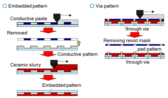 | Figure 5. Schematic illustration of the fabrication process for the embedded pattern sheet |
The patterned sheets were laminated and stacked by heat press. These multilayered structures had 20 layers including 19 layers for forming 18 turns three-dimensional structure coil. Top layer was the ferrite sheet without the coil pattern. The multilayered structures were diced excess ferrite part around the coil pattern. These specimens were fired and it formed the outside electrode. Through these processes, the multilayered ceramic coil with the three-dimensional structure and magnetic core was achieved. Figure 6 shows the fabrication process of the ceramic coil.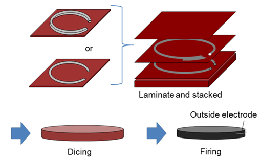 | Figure 6. Fabrication process for the ceramic coil structure |
2.4. Power Transfer Experiment
The fabricated ceramic coils are measured transfer voltage. Figure 7 shows the arrangement of power transfer experiment. In this figure, the transmitter coil and receiver coil were placed in facing each other. A plastic board was lying between two coils, and a resistance of 50Ω was connected to the receiver coil. The output voltage was measured by an oscilloscope. Transmitter coil was fabricated by winding wire. The turn number of the transmitter coil was 15. The inputted voltage and the inputted frequency were 8V and 100 kHz, respectively.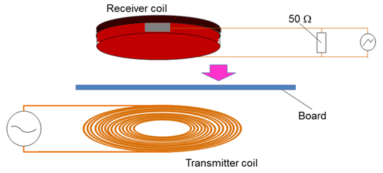 | Figure 7. Arrangement of power transfer experiment |
3. Results
Multilayer ceramic coils that had the surface coil pattern, the embedded coil pattern and screen printing coil pattern were fabricated. Additionally, the fabricated coils were wireless power transmitted.
3.1. Evaluation of Coil Patterns
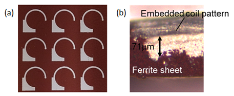
Figure 8 shows the observation of the surface coil pattern before firing. In this figure, (a) shows overall view of the pattern, and (b) is cross-sectional view. In the overall view, the coil pattern was clear. The thickness of the pattern was 68 μm. The deformation was not observed in the achieved surface pattern. Figure 9 shows the overall view (a) and cross-sectional view (b) of the embedded coil pattern before firing. In the overall view, the coil pattern was also clear, and the surface showed flat. The thickness of the pattern was 71 μm. The deformation was not observed in the achieved embedded pattern at the side of the conductor.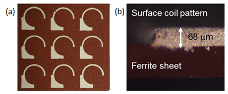 | Figure 8. Observation of surface coil pattern before firing (a) overall view (b) cross-sectional |
 | Figure 9. Observation of embedded coil pattern before firing (a) overall view (b) cross-sectional view |
3.2. Multilayer Ceramic Coil for Wireless Power Transfer
The ceramic sheets with the coil patterns by the photo resist film were stacked and fired. Diameter and height of surface pattern coil were 5.3 mm and 2.5 mm, respectively. Diameter and height of embedded pattern coil were 5.2 mm and 2.2 mm, respectively. Figure 10 shows the cross-sectional view of each patterned coil. The thickness of the surface pattern and embedded pattern were 46.7 μm and 48.0 μm, respectively. Inductance and internal resistance of the surface pattern coil were 91.1 μH, and 0.78Ω, respectively. Inductance and internal resistance of the embedded pattern coil were 98.5 μH and 0.75 Ω, respectively. 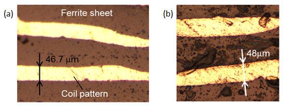 | Figure 10. Cross-sectional view of each patterned coil |
Fabricated ceramic coils that were patterned by the photo resist film were compared with the conventional screen printing coil. Thickness of the coil pattern and internal resistance of the screen printing ceramic coil were 33.0 μm and 0.97 Ω, respectively. By these results, the patterning process that the photo resist film was used for holding the conductive paste can form the high-aspect-ratio conductive pattern. Moreover, high-aspect-ratio pattern decrease the internal resistance.
3.3. Results of Wireless Power Transfer Experiment
Results of the wireless power transfer experiment are shown in figure 11. Transmitted results of each fabricated ceramic coil are shown in table 2. By these results, the ceramic coil that has three-dimensional structure and magnetic material showed wireless power transfer. And then, the embedded pattern coil showed higher transmitted voltage. To achieve high transmitted efficiency, lower internal resistance is required. Therefore, the embedded pattern has advantage forming high-aspect-ratio pattern. Moreover, when the pattern is embedded in the ceramic sheet, thickness of magnetic material between each coil conductor becomes thin. The thin magnetic material suppresses the magnetic flux loss that introduces magnetic material. Figure 12 shows the result of FEM analysis of the magnetic flux in the magnetic material.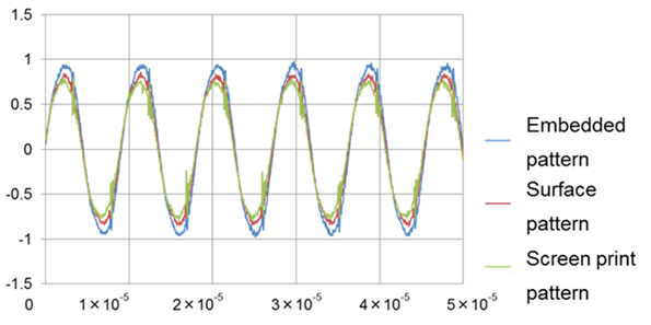 | Figure 11. Results of the wireless power transfer experiment |
Table 2. Description of the samples
 |
| |
|
 | Figure 12. Results of FEM analysis of the magnetic flux in the magnetic material |
ACKNOWLEDGMENTS
The sample of this study was fabricated by the facility at the Research Center for Micro Functional Devices, Nihon University. The part of this study was supported by the CST research project of Nihon University and The Foundation for Technology Promotion of Electronic Circuit Board.
References
| [1] | Tai Y-C., Fan L-S., and Muller R. S., (1989) IC-processed micro-motors: design, technology, and testing. Proc. IEEE Micro Electro Mechanical Systems. An Investigation of Micro Structures, Sensors, Actuators, Machines and Robots, Salt Lake City, 1989, pp. 1–6. |
| [2] | Renaud, M., Sterken, T., Schmitz, A., Fiorini, P., Hoof C. V., and Puers, R., (2007) “Piezoelectric Harvesters and MEMS Technology: Fabrication, Modeling and Measurements.” Proc. of in The 14th International Conference on Solid-State Sensors, Actuators and Mycrosystems, June, pp. 891-894. |
| [3] | Steyn, J. L., Kendig, S. H., Khanna, R., Umans, S. D., Lang J. H., and Livermore, C., (2009). A Self-EXcited MEMS Electro-Quasi-Static Induction Turbine Generator. J. Microelectromech. S., 18 (2), pp. 424-432. |
| [4] | Jones, P G., Beeby, S. P., and White, N. M., (2001) Towards a Piezoelectric Vibration-Powerd Microgenerator. IEE Proc. Sci., Meas. Technol., 148 (2), March, pp. 68-72. |
| [5] | Yan, G., Ye, D., Zan, P., Wang, K., and Ma, G., (2007). Micro-Robot for Endoscope Based on Wireless Powe Transfer. Proc. of International Conference on Mechatronics and Automation, August. pp. 3577-3581. |
| [6] | Takato M., Nishi T., Kaneko M., Tanida J., Tada S., Saito K. and Uchikoba F. (2014) Multilayer Ceramic Coil for Wireless Power Transfer System by Photo Resist Film Process. Proc. of International Conference on Electronics Packaging, April. pp. 326-331. |


 Abstract
 Reference
 Full-Text PDF
 Full-text HTML