-
Paper Information
- Paper Submission
-
Journal Information
- About This Journal
- Editorial Board
- Current Issue
- Archive
- Author Guidelines
- Contact Us
International Journal of Materials Engineering
p-ISSN: 2166-5389 e-ISSN: 2166-5400
2016; 6(5): 155-158
doi:10.5923/j.ijme.20160605.03

Preparation of ZnO Thin Film by Development Low-Pressure High-Frequency Plasma Chemical Vapor Deposition System
 Abstract
 Reference
 Full-Text PDF
 Full-text HTML
Thaweesak Tanaram1, Nuttee Thungsuk2, Harittapak Apirat3, Narong Mungkung4, Yoshimi Okamura5, Toshifumi Yuji5
1Faculty of Industrial Technology, Pibulsongkram Rajabhat University, Phitsanulok, Thailand
2Department of Electrical Engineering, Dhonburi Rajabhat University Samut-Prakan, Samut-Prakan, Thailand
3Faculty of Science and Technology, Dhonburi Rajabhat University, Thailand
4Department of Electrical Technology Education, King Mongkut's University of Technology Thonburi, Bangkok, Thailand
5Faculty of Education & Culture, University of Miyazaki, Miyazaki, Japan
Correspondence to: Nuttee Thungsuk, Department of Electrical Engineering, Dhonburi Rajabhat University Samut-Prakan, Samut-Prakan, Thailand.
| Email: |  |
Copyright © 2016 Scientific & Academic Publishing. All Rights Reserved.
This work is licensed under the Creative Commons Attribution International License (CC BY).
http://creativecommons.org/licenses/by/4.0/

This research paper aims to present the development of low-pressure high-frequency plasma chemical vapor deposition system for preparation of Zinc oxide (ZnO) thin film on silicon wafer, B-doped p-type Si (100) wafer, with powder deposition. The plasma system for this experimental used mixture of argon (Ar) and oxygen (O2) gas at 10 L/min. and 2 L/min., respectively. The ZnO thin film was performed by heating the ZnO powder. The Ar and O2 gas have been heating in pipe with silicone belt heater and micro gas heater. The temperature was controlled by temperature control (PID). The ZnO thin film was investigated by using contact angle meter and scanning electron microscope (SEM) to confirm the formation of ZnO thin film on the substrate. The results from the contact angle meter confirmed that the Si wafer with ZnO thin film showed an increased in hydrophobic property compared to the traditional Si wafer. In addition, the results from SEM confirmed that the formation of ZnO thin film on surface was in typical pyramid shape structure with crystal grain size about 100–120 nm.
Keywords: Zinc Oxide, Plasma CVD, Scanning electron microscope (SEM), Thin film
Cite this paper: Thaweesak Tanaram, Nuttee Thungsuk, Harittapak Apirat, Narong Mungkung, Yoshimi Okamura, Toshifumi Yuji, Preparation of ZnO Thin Film by Development Low-Pressure High-Frequency Plasma Chemical Vapor Deposition System, International Journal of Materials Engineering , Vol. 6 No. 5, 2016, pp. 155-158. doi: 10.5923/j.ijme.20160605.03.
Article Outline
1. Introduction
- Zinc Oxide (ZnO) has been interesting in the cluster of semiconductor because of many advantages such as high transmission and a good conductor [1]. ZnO is N-type semiconductor with a wide band gap material, 3.37 eV direct band gap at room temperature, and a high excitation binding energy of 60 meV [2]. Therefore, the ZnO was applied to use as transducers, luminescent materials, transparent conductors, photo detectors, heat mirrors, varistors, optical modulator waveguides, gas sensors and solar cells [3, 4].There are many systems from ZnO thin film such as chemical vapor deposition, Radio-frequency (RF) magnetron sputtering, spray pyrolysis, pulsed laser deposition, sol–gel-dip-coating, electro-deposition, metal–organic chemical vapor deposition (MOCVD), molecular beam epitaxy(MBE) [5, 6]. The most popularsystem for thin film formation is RF- magnetron sputtering but the disadvantage of this system is imperfection of film structural and instability of the electrical properties of the film [7]. On the other hand, plasma chemical vapor deposition (Plasma CVD) can from the thin film complety at low temperature [8].In this research, the development low-pressure high-frequency plasma chemical vapor deposition system for preparation of ZnO thin film on silicon wafer B-doped p-type Si (100) wafer was presented. The plasma equipment with suitable for ZnO thin film formation was developed. The ZnO thin film was simply investigated using contact angle meter and scanning electron microscope (SEM) for basic analysis of ZnO thin film.
2. Experimental Setup
- Fig. 1 Shows the system of low-pressure high-frequency plasma chemical vapor deposition for preparation of ZnO thin film. The main component of plasma CVD system were plasma chamber, matching box, RF-power, vacuum pump, gas heater, ZnO powder, Temperature control, mass flow controller and gas supply. The vacuum chamber of plasma CVD system was composed of stain steel (SUS316), with a diameter of 430 mm and high of 180 mm. The diameter of the electrode for generating plasma process was 200 mm. The distance between upper and lower plasma electrodes was 20 mm. The showerhead and gas distribution plate had 145 fine pores arranged in the shape of grid. The distance between each pore was 12 mm. The diameter of each pore was 1.0 mm.
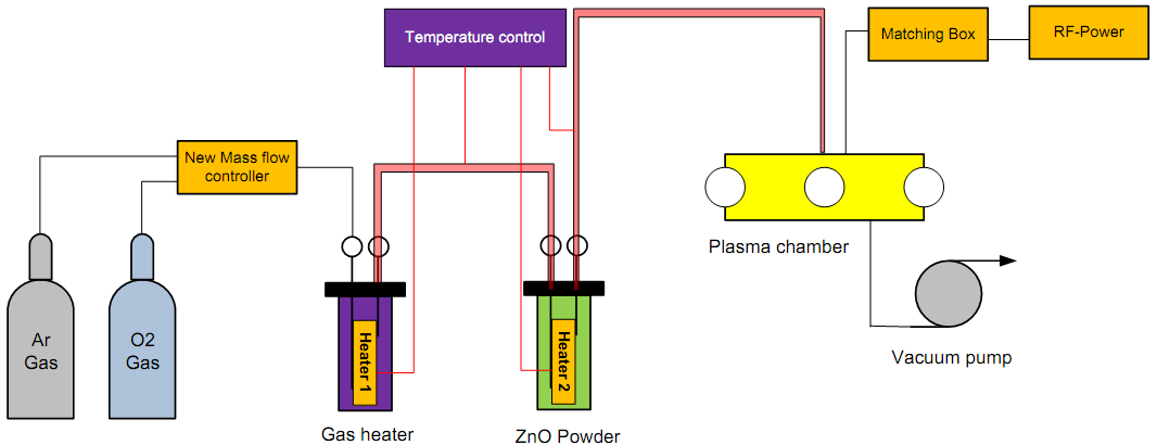 | Figure 1. The system of low-pressure high-frequency plasma CVD for preparation of ZnO thin film |
3. Results and Discussion
- Fig. 2 shows plasma emission in vacuum chamber during ZnO deposition by low-pressure high- frequency plasma CVD method at eyehole width of 75 mm. the area between upper and lower plasma electrode of 20 mm. Fig. 2a shows plasma phenomenon from ZnO powder source during ZnO deposition at the plasma power of 300 W., vacuum level of 3.2×10² Pa., temperature of 300C and Ar gas flow rate of 10 L/min. while Fig. 2b shows plasma phenomenon at gas mixture of Ar and O2 gas at 10 L/min. and 2 L/min., respectively when plasma power, vacuum level and temperature was maintained. The plasma phenomenon in Fig. 2a and Fig. 2b were different from the observation with bare eyes. Fig. 2a and Fig. 2b showed plasma color in blue and red, respectively. It was found that when increasing ZnO powder source with the mixture of Ar and O2 gas into low-pressure high- frequency plasma CVD method resulted in plasma phenomenon was red color, in addition non ZnO powder source when surface treatment with the mixture of Ar and O2 gas only was violet color [9].
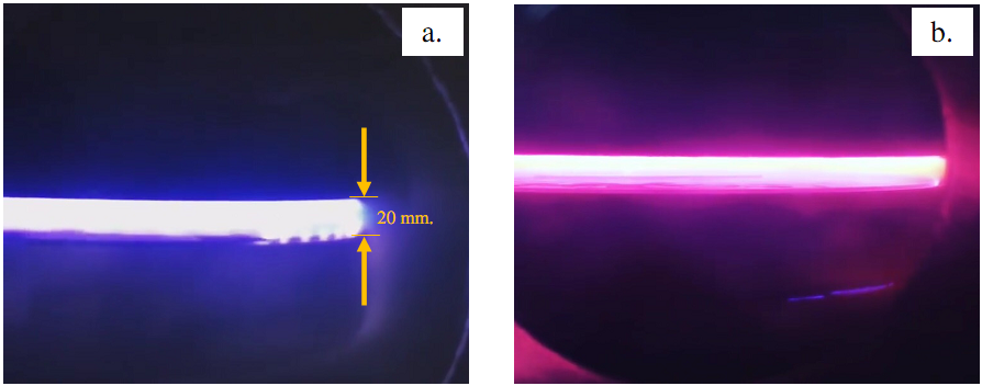 | Figure 2. Plasma phenomenon a) Ar gas flow rate b) a mixture of Ar and O2 gas |
- Fig. 3 shows the action of a water droplet dropped down onto a B-doped p-type Si (100) wafer with contact angle meter using the θ/2 method with the 1 μL. pure water droplet. Fig. 3a and Fig. 3b were the change of a water droplet of the original silicon wafer surface and the surface of ZnO thin film on silicon wafer from low-pressure high-frequency plasma chemical vapor deposition system under the condition as in Fig 2b, respectively. It was found that the contact angle of original silicon wafer surface and surface of ZnO thin film from plasma deposition was 35.8 and 81.1 degree, respectively. The hydrophobic properties at the surface of ZnO thin film increased from the plasma deposition. The contact angle of the original silicon wafer surface and surface of ZnO thin film were difference about 45 degree due to surface topography and microstructure and chemical composition on substrate with ZnO thin film [10].
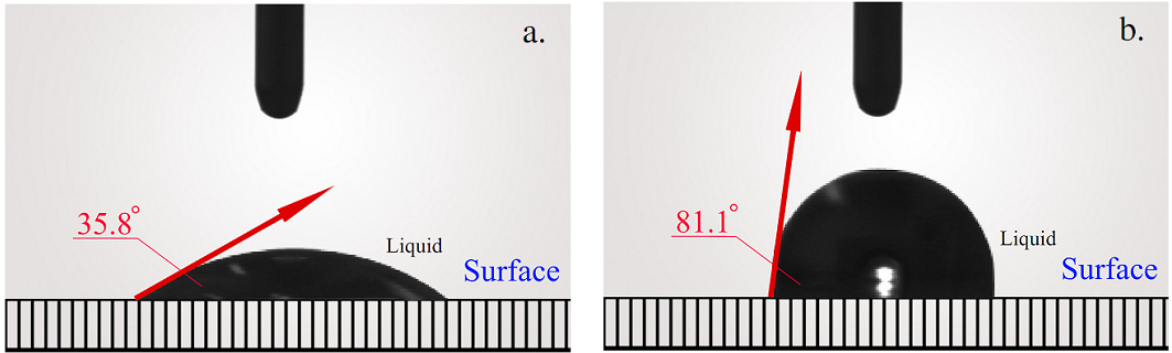 | Figure 3. The action of a water droplet on silicon wafer a) The original silicon wafer surface b) The ZnO thin film on silicon wafer surface |
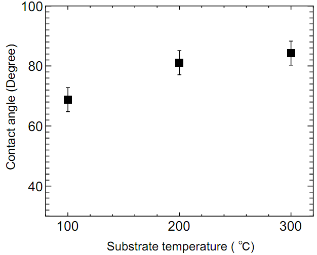 | Figure 4. The relationship between the contact angles and the temperature of substrate |
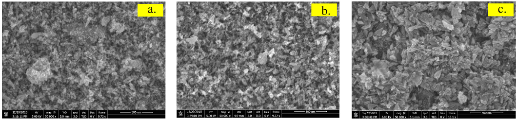 | Figure 5. The SEM image of the ZnO thin film on silicon wafer a) 100C b) 200C c) 300C |
4. Conclusions
- The preparation of ZnO thin film was successfully performed by developed the low-pressure high-frequency plasma CVD system with powder deposition. The results were investigated by measuring the surface of ZnO thin film from ZnO powder deposition. The contact angle meter confirmed that the hydrophobic properties changed. The contact angle increased compared with the original silicon wafer, confirming the formation of ZnO thin film on the silicon wafer surface as a result of the crystal grain of ZnO formation on surface. In addition, when deposition temperature increased, the hydrophobic properties changed, the angle of water droplet increased due to the changed of grain size of ZnO thin film on surface. The results from scanning electron microscope (SEM) also confirmed that the morphology ZnO thin film on surface changed to typical pyramid shape structure with larger of crystal grain size.
ACKNOWLEDGMENTS
- This work has been supported by Pibulsongkram Rajabhat University (PSRU) Research fund, Thailand. The authors would like to thank Plasma laboratory of University of Miyazaki for place of experiment.