International Journal of Materials Engineering

p-ISSN: 2166-5389    e-ISSN: 2166-5400

2013;  3(4): 59-65

doi:10.5923/j.ijme.20130304.01

Electrical Properties of ZnO/p-Si Heterojunction for Solar Cell Application

F. Z. Bedia, A. Bedia, D kherbouche, B. Benyoucef

URMER, Abou-Bakr Belkaid University, 13000, Tlemcen Algeria

Correspondence to: F. Z. Bedia, URMER, Abou-Bakr Belkaid University, 13000, Tlemcen Algeria.

Email:

Copyright © 2012 Scientific & Academic Publishing. All Rights Reserved.

Abstract

in this study, we report the ZnO thin films prepared by spray pyrolysis method at 550C° with good transparency in the visible region. The ZnO film was deposited on Si substrates to from the n-Zn0/ p-Si heterojuction. The morphology and electrical properties of the films have been carried out by means of scanning electron microscopy (SEM) and I-V measurements. The current-voltage characteristic of the n-Zn0/ p-Si heterojunction device measured at room temperature in the dark and under illumination (lamp/160 W).

Keywords: ZnO Thin Film, ZnO/p-Si Heterojunction, Electrical Properties

Cite this paper: F. Z. Bedia, A. Bedia, D kherbouche, B. Benyoucef, Electrical Properties of ZnO/p-Si Heterojunction for Solar Cell Application, International Journal of Materials Engineering , Vol. 3 No. 4, 2013, pp. 59-65. doi: 10.5923/j.ijme.20130304.01.

1. Introduction

ZnO is a promising semiconductor material for various optoelectronic applications such as thin film solar cell[1], transparent conducting electrodes[2], light-emitting diodes (LEDs)[3], due to its large direct bandgap (3.37 eV) and exciton binding energy (60 meV) at room temperature. Many techniques, such as reactive evaporation[4], chemical vapor deposition (HVP-CVD)[5], sol-gel spin coating method[6] spray pyrolysis[7] magnetron sputtering[8], have been developed and used to grow ZnO on a variety of substrates for fabrication heterojunction structure.
Heterojunction solar cells consisting of a wide band gap transparent conductive oxide (TCO) on a single crystal silicon wafer have a number of potential advantages such as an excellent blue light response, simple processing steps, and low processing temperatures[9]. One promising type of TCO/Si solar cells uses undoped ZnO on Si wafer. ZnO/Si heterojunctions are of particular interest in the integration of optoelectronic devices utilizing the hybrid advantages of the large exaction binding energy of the ZnO thin film and the cheapness of Si substrates. However, there are a few reports on the n-ZnO/p-Si heterojunction where the ZnO film is grown by different techniques.
For instance, Ajimsha and al[10] reported the electrical characteristics of n-ZnO/p-Si heterojunction diodes grown by pulsed laser deposition at different oxygen pressures. Sun[11] achieved UV electroluminescence (EL) emission from ZnO nanorods with n-ZnO/p-Si heterojunction structure fabricated by the hydrothermal method. Baik et al [12] have prepared ZnO/n-Si junction solar cells with conversion efficiency of 5.3% by sol-gel method, and studied the effect of surface-doping concentration on the ZnO/n-Si solar cells, by using the phosphor silicate glass films. Moreover, zinc oxide/n-Si junction solar cells produced by spray pyrolysis method with relatively high conversion efficiency 6.9% to 8.5% have been achieved by Kobayashi et al.[13]. The conversion efficiency of ZnO/Si solar cell depends greatly on the properties of ZnO films, depending on the growth conditions including deposition temperature, growth pressure and deposition time. Many researchers have found that the electrical properties strongly depend on the thickness of ZnO films.[14],[15] for application in optoelectronic devices, the optimum film thickness should be chosen for the best device performance.
In this study, we report n-type behavior of ZnO thin film based on ZnO/p-Si heterojunction solar cells, where the type n ZnO film is prepared by spray pyrolysis. We describe the electrical properties of ZnO/Si heterojunction solar cells.

2. Experimental

ZnO thin films were grown on p-type silicon (111) and glass substrates by spray pyrolysis method. The spray solution is prepared by dissolving 0.085 mol zinc acetate dehydrated (Zn (CH3COO)2· 2H2O) in methanol (CH3OH). Compressed ambient air is used to atomize the solution. The flow rate is kept about 5ml/1min during preparation of samples. The nozzle-substrate distance is maintained at 27 cm and the substrate temperature is fixed at 550°C and controlled within ±5°C by using an electronic temperature controller 38XR-A Digital Multimeter kept on the metallic hot plate surface. Then the substrates are regularly heated up to the required temperature, before being sprayed on. Then the films are annealing at 550°C for 1 h in order to eliminate organic products.
The film was found to be n-type by using a hot-probe method. The Cu metal contact was deposited on the ZnO layer and the backside of the Si substrate to form electrodes of the p-n diode.
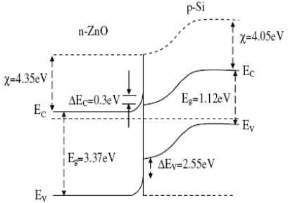
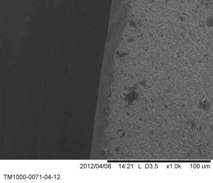
The distance of the Cu contacts on ZnO film is 1 mm. The schematic structure of the ZnO/p-Si heterojunction is shown in figure 1. A pair of contacts was made on the backside of a separate piece of the sample to check for Ohmic contact formation. The morphology of the fabricated ZnO thin film was observed in a scanning electron microscope (SEM). The surface morphologies of ZnO thin film grow on p-Si wafer by spray pyrolysis are shown in Figure 2.
Figure 1. Band gap structure of the n-ZnO/p-Si heterojunction
Figure 2. SEM micrographs of ZnO film grown on p-Si wafer
The electrical properties of ZnO thin film was characterized by two point probe at room temperature. The current–voltage characteristic of the device was measured by 38XR-A Digital Multimeter semiconductor parameter analyzer. The figure 1 shows the energy band diagram of the heterojunction at equilibrium. The energy band diagram was constructed based on Anderson’s model[16]. The band gap and electron affinity values for ZnO and Si are assumed to be EgZnO = 3.37 eV, χZnO = 4.35 eV[17] and EgSi = 1.12 eV, χSi =4.05 eV[18], respectively. The left side region represents n-type ZnO thin film and the right side is p-type Si substrate.

3. Results and Discussion

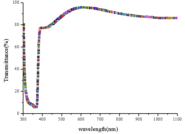
The transmittance spectra of the ZnO film was measured in the wavelength range 300–800 nm at room temperature, as shown in Fig. 3. At short wavelengths, it observed low transmission values because of its high absorbing properties. At long wavelengths the transmission values are high due to non-existence of absorption. The transmittance in this region varies between 70 and 90%. In addition, the ZnO film is opaque material in Ultra-violet region and transparent in visible region. Similar behaviour has also reported in literature[19].
The refractive index n is an important parameter for optical materials and applications. The expression for refractive index is given by
(1)
where;
(2)
and ns is the refractive index of the glass substrate. The refractive index n calculated using equation 1 equal to 2.03. This value is in a good agreement with to theoretical refractive index of ZnO film in the visible region (n = 2).
The thickness of the films was calculated using the equation by
(3)
where n1 and n2 are the refractive indices corresponding to wavelengths λ1 and λ2, respectively. The thickness of ZnO film is calculated about 1.3µm.
The optical energy gap of the ZnO film grow on glass substrate was determined by Tauc law in a direct transition between valence and conduction bands from the expression[20]:
(4)
Where A is a constant, hν is the photon energy , Eg is the optical energy band and m is an index that characterizes the optical absorption process. The exponent m depends on the nature of the transition, m = 1/2, 2, 3/2, or 3 for allowed direct, allowed nondirect, forbidden direct, or forbidden nondirect transitions, respectively[21]. It is well known that ZnO has an allowed direct band gap and m = 1/2 was used for the band gap calculation.
Figure 3. Transmission spectra of ZnO thin film grow on glass
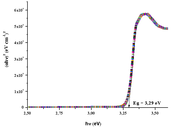
Figure 4. The plots of (αhν)2 as function of photon energy of the ZnO
Fig.4 shows plot of (αhv)2 versus (hv) where the optical band gap of the film was determined by extrapolating the linear region to (αhν)2 = 0. Optical energy gap of ZnO film was calculated as 3.29 eV. This value was smaller to the band gap of intrinsic ZnO which is 3.37 eV[19]. The optical band gap is in good agreement with that of ZnO thin film prepared by spray pyrolysis[19].
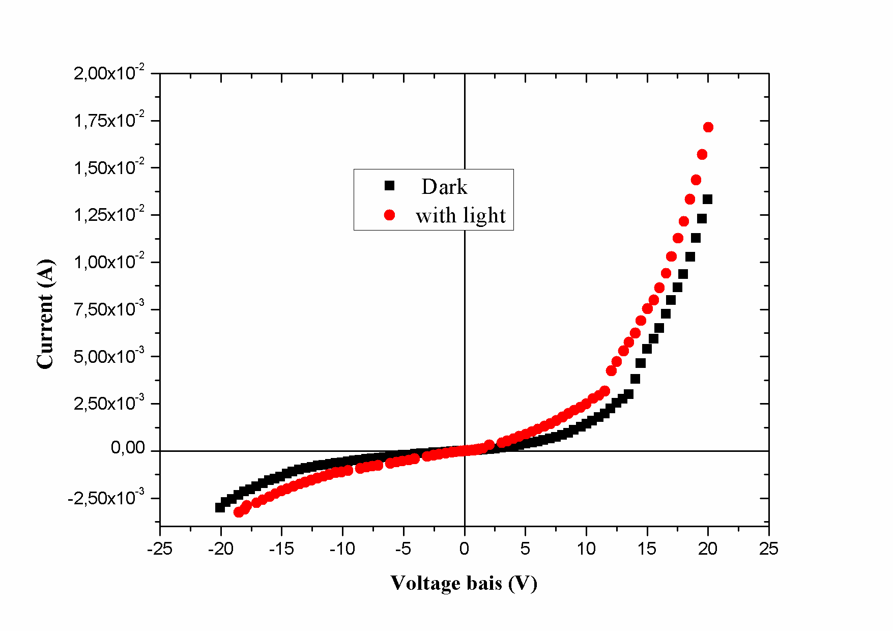
Figure 5 shows the current–voltage characteristic of the ZnO/ p-Si heterojunction measured in the dark and under illumination at room temperature. The current values increase exponentially with increasing in the forward bias voltage. The turn-on voltage is around 11.5 V for the forward bias and a reverse bias breakdown voltage of 12.5V as seen from the I-V curve in the dark. Moreover, it is seen from the figure the device has high forward current that reverse current. The rectification ratio IF/IR (IF and IR stand for forward and reverse current, respectively) of the structure at 20 V is found to 4.
According to the p–n junction theory, the standard diodes I–V relation[22]
(1)
Where V is voltage bias and Is is saturation current wich derived from the straight line intercept of ln I at V = 0 and is given by:
(2)
With q electronic charge, kB Boltzman constant, A* the effective Richardson constant taken as 32 A cm−2 K−2 for ZnO[23], S the area of the diode and qΦb the barrier height (eV). Here, n is the quality factor that measures the conformity of the diode to pure thermionic emission, which is given by:
(3)
The value of the ideality factor of the heterojunction is determined from the slop of the straight line region of the forward bias ln (I) -V characteristics. The typical values of the ideality factors and the reverse saturation current are 5.12 and 8.01×10⁻⁸ A, respectively. The saturation current Is is comparable to P.Klason et al.[24] value 6.53×10⁻⁸A and to the value 1.78×10⁻⁷ A reported by N. Zebbar et al.[25] for an-ZnO/p-Si heterojunction. The ideality factor is larger than the latter value (2). This indicates that the diode exhibits a non-ideal behavior due to the oxide layer and the presence of surface states[26]. This is rather close to the previous reported values of 5.47[26] and 5.1[27]. Values of the saturation current I0 were obtained by extrapolation of the linear region of the semi-logarithmic forward I–V curves to zero applied voltage and were used to calculate the apparent barrier height by the following function:
(4)
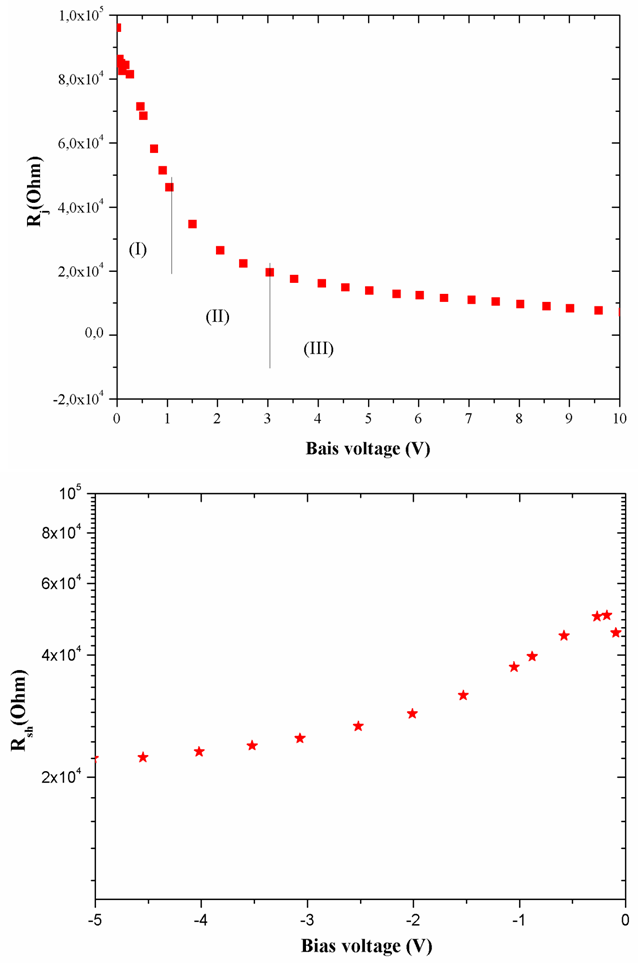
In the study, the calculated potential barrier height value at room temperature is 0.57 eV. This value is according with 0.6 eV[28] reported by other authors. In reality, the I-V behavior of the diode is affected by parasitic resistances such as series resistance (Rs) related to the interfaces between two semiconductors and shunt resistance (Rsh) due to semiconductor electrode interface properties[29]. Thus, it is important to determine these parameters. The junction resistance Rj for the diode is expressed as
(5)
Figure 5. I–V characteristics curves ZnO/p-Si heterojunction in dark and in light (light 160W white lamp)
Figure 6. (a) junction resistance RJ as a function of forward bias. (b) junction resistance RJ as a function of reverse bias
Therefore, Rs and Rsh values can be easily determined from the plot of Rj vs. V At higher forward voltages, Rj value approaches to a constant value corresponding to Rs. Whereas, at higher reverse voltages, the Rj value becomes nearly Rsh[30]. It is worth noting that series and shunt resistances are important parameters for solar cells characterization. In Figure 6 we have drawn the calculated Rs and Rsh of diode junction, for forward bias and reverse bias, respectively. Figure 6-(a) shows roughly three regions correspondents to the previous (I), (II) and (III) regions. In the region (I) (V < 1V) the RJ value decreases abruptly with the applied bias, whereas, in the region (II) (1V < V< 3V), RJ decreases more gradually, and in region (III) (V > 3 V) it reaches a saturation value Rs equal to 6.63 k.Ω. This value corresponds to the series resistance of the heterojunction, which is mainly due to the ZnO thin film resistance at room temperature. However, in the case of reverse voltage region, the RJ represents the shunt resistance Rsh of the heterojunction. This value decreases gradually with the applied bias and it saturates to 2.27x10⁻⁵ Ω. The shunt resistance originates from the surface, bulk and grain boundaries carriers recombination[25].
The I–V characteristics were measured under illumination by power white light (160 W) lamp, as shown in figure 5. Typical good rectifying and photoelectric behavior were observed for the device. The dark leakage current is small, whereas its photocurrent generated under illumination is higher. It is observed that the heterojunction exhibits a rectifying behavior in the presence of light too. Under reverse bias conditions photocurrent caused by the n-ZnO /p-Si heterojunction irradiated under illumination by white light lamp was evidently much larger than the dark current. For example, when the reverse bias is -18 V, the dark current is only 2.17×10⁻³ A. While the reverse-bias photocurrent reach to 3.08×10⁻³ A under lamp illumination. Figure 5 shows the n-ZnO /p-Si heterojunction under white lamp illumination has great photovoltaic effect. The photovoltage of the heterojunction is 6 mV and the short circuit current is 4 µA. Majority carriers are blocked from tunneling by the band gap of n-ZnO. Tunneling can also occur via defects states at the interface, we regard JST to be the dominant tunnel transition via defects in ZnO -Si, where JST is the tunnel transition current. The photoelectric effect in the structure is because of the light-induced electron generation at the depletion region of the structure [2].

4. Conclusions

The current–voltage (I–V) characteristics of the p–n heterostructure show nonlinear diode like behavior. We calculated the ideality factor and the saturation current are 5.12 and 8.01×10⁻⁸A, respectively. The ideality factor is higher than 2, indicating that the diode exhibits a non-ideal behavior due to the oxide layer and the presence of surface states. The heterojunction shows great photoelectric effect under power (160W) lamp illuminate. The photocurrent responses were detected for the solar cell. The solar cell exhibited a short-circuit current density of 4×10⁻³ mA, an open-circuit voltage of 6mV. Doping studies and fine tuning of the junction morphology will be necessary to further improve the performance of ZnO/Si heterojunction solar cells.

References

[1]  Shin, B.K., Lee, T.I., Xiong, J., Hwang, C., Noh, G., Cho, J.H. and Myoung, J.M., 2011, Bottom-up grown ZnO nanorods for an antireflective moth-eye structure on CuInGaSe2 solar cells, J. Solar Energy Materials & Solar Cells, 95, 2650-2654.
[2]  Ootsuka, T., Liu, Z.,. Osamura, M, Fukuzawa, Y., Kuroda, R., Suzuki, Y., Otogawa, N., Mise, T., Wang, S., Hoshino, Y., Nakayama, Y., Tanoue, H. and Makita, Y., 2005, Studies on Aluminum-doped ZnO films for transparent electrode and antireflection coating of β-FeSi2 optoelectronic devices, Thin Solid Films, 476, 30-34.
[3]  Szarko, J.M., Song, J.K., Blackledge, C.W., Swart, I., Leone, S.R., Li, S. and Zhao, Y., 2005, Optical injection probing of single ZnO tetrapod lasers, Chemical Physics Letters, 404, 171-176.
[4]  Al Asmar, R., Atanas, J.P., Ajaka, M., Zaatar, Y., Ferblantier, G., Sauvajol, J.L., Jabbour, J., Juillaget, S. and Foucaran, A., 2005, Characterization and Raman investigations on high-quality ZnO thin films fabricated by reactive electron beam evaporation technique. Journal of Crystal Growth, 279 , 394-402.
[5]  Barnes, T.M., Leaf, J., Hand, S., Fry, C. and Wolden, C.A., 2004. Room temperature chemical vapor deposition of c-axis ZnO. Journal of Crystal Growth, 274, 412–417.
[6]  Chen, S., Zhang, J., Feng, X., Wang, X., Luo, l., Shi, Y., Xue, Q., Wang, C., Zhu, J.and Zhu, Z., 2005, Nanocrystalline ZnO thin films on porous silicon/silicon substrates obtained by sol–gel technique, Applied Surface Science, 241, 384–391.
[7]  Ayouchi, R., Leinen, D., Martın, F., Gabas, M., Dalchiele, E. and Ramos-Barrado, J.R., 2003, Preparation and characterization of transparent ZnO thin films obtained by spray pyrolysis. Thin Solid Films, 426, 68–77.
[8]  Chaabouni, F., Abaab, M. and Rezig, B., 2006, Characterization of n-ZnO/p-Si films grown by magnetron sputtering, Superlattices and Microstructures, 39, 171–178.
[9]  Kobayashi, H., Kogetsu, Y., Ishida, T., and Nakato, Y., 1993, Increases in photovoltage of ‘‘indium tin oxide/silicon oxide/mat-textured n-silicon’’ junction solar cells by silicon preoxidation and annealing processes. J. Appl. Phys, 74, 4756.
[10]  Ajimsha, R.S., Jayaraj, M.K and Kukreja, L.M., 2008, Electrical Characteristics of n-ZnO/p-Si Heterojunction Diodes Grown by Pulsed Laser Deposition at Different Oxygen Pressures. Journal of Electronic Materials, 37, 770–775.
[11]  Sun, H., Zhang, Q.F and Wu, J. L, 2006, Electroluminescence from ZnO nanorods with an n-ZnO/p-Si heterojunction structure . Nanotechnology, 17, 2271–2274.
[12]  Baik, D.G. and Cho, S.M., 1999, Application of sol-gel derived films for ZnO/n-Si junction solar cells, Thin Solid Films, 354-227.
[13]  Kobayashi, H., Mori, H., Ishida, T. and Nakato, Y.J., 1995, Zinc oxide/n-Si junction solar cells produced by spray-pyrolysis method. J. Appl. Phys, 77, 1301.
[14]  Kishimoto, S., Yamamoto, T., Nakagawa, Y., Ikeda, K., Makino, H. and Yamada, T., 2006, Dependence of electrical and structural properties on film thickness of undoped ZnO thin films prepared by plasma-assisted electron beam deposition. Superlattices and Microstructures, 39,306–313.
[15]  Dong, B. Z., Fang, G. J., Wang, J. F., Guan, W. J. and Zhao, X. Z., 2007, Effect of thickness on structural, electrical, and optical properties of ZnO: Al films deposited by pulsed laser deposition. Appl. Phys., 101, 033713.
[16]  Du, G., Cui, Y., Xiaochuan, X., Li, X., Zhu, H., Zhang, B., Zhang, Y. and Ma, Y., 2007, Visual-infrared electroluminescence emission from ZnO/GaAs heterojunctions grown by metal-organic chemical vapor deposition. Appl. Phys. Lett., 90, 243504.
[17]  Dutta, M. and Basak, D., 2008. p-ZnO/n-Si heterojunction: Sol-gel fabrication, photoresponse properties, and transport mechanism. Appl. Phys. Lett., 92 , 212112.
[18]  Sze, S.M., 1981.Physics of Semiconductor Devices. 2nd Edn., John While and Sons
[19]  Ocak, Y. S., 2012. Electrical characterization of DC sputtered ZnO/p-Si heterojunction. Journal of Alloys and Compounds, 513, 130-134.
[20]  J.I. Pankove, Optical Processes in Semiconductors, Prentice - Hall Inc, Englewoord Cliffs, NJ, 1971.
[21]  I.S. Yahia, Farag, A.A.M., Cavas, M. and Yakuphanoglu, F., 2013, Effects of stabilizer ratio on the optical constants andoptical dispersion parameters of ZnO nano-fiber thin films. Superlattices and Microstructures, 53, 63–75.
[22]  Pierret R.F. Semiconductor Device Fundamentals, Addison - Wesley, 1996.
[23]  Singh, C.S., Agarwal, G., Durga Rao G., Chaudhary S., Singh, R., 2011, Effect of hydrogen peroxide treatment on the electrical characteristics of Au/ZnO epitaxial Schottky diode. Materials Science in Semiconductor Processing, 14, 1–4.
[24]  Klason, P., Rahman, M.M., Hu, Q.H., Nur, O., Turan, R. and Willander, M., 2009, Fabrication and characterization of p-Si/n-ZnO heterostructured junctions. Microelectronics Journal, 40, 706–710.
[25]  Zebbar, N., Kheireddine, Y., Mokeddem, K., Hafdallah, A., Kechouane, M. and Aida, M.S., 2011.Structural, optical and electrical properties of n-ZnO/p-Si heterojunction prepared by ultrasonic spray. Materials Science in Semiconductor Processing, 14,229–234.
[26]  Yakuphanoglu, F., Caglar, Y., Caglar, M. and Ilican, S., 2010, ZnO/p-Si heterojunction photodiode by sol–gel deposition of nanostructure n-ZnO film on p-Si substrate, Materials Science in Semiconductor Processing, 13,137–140.
[27]  Majumdar, S., Banerji, P., Majumdar, S. and Banerji, P., 2009, Temperature dependent electrical transport in p-ZnO/n-Si heterojunction formed by pulsed laser deposition, J. Appl. Phys.
[28]  Farag, A.A.M., Farooq, W.A., Yakuphanoglu, F., 2011, Characterization and performance of Schottky diode based on wide band gap semiconductor ZnO using a low-cost and simplified sol–gel spin coating technique, Microelectronic Engineering, 88, 2894–2899.
[29]  Nelson, J., 2003, The Physics of Solar Cells. Imperical College Press, UK.
[30]  Mansour, Sh. A. and Yakuphanoglu, F., 2012, Electrical - optical properties of nanofiber ZnO film grown by sol gel method and fabrication of ZnO/p-Si heterojunction. Solid State Sciences, 14, 121-126.