-
Paper Information
- Previous Paper
- Paper Submission
-
Journal Information
- About This Journal
- Editorial Board
- Current Issue
- Archive
- Author Guidelines
- Contact Us
International Journal of Materials Engineering
p-ISSN: 2166-5389 e-ISSN: 2166-5400
2013; 3(1): 4-10
doi:10.5923/j.ijme.20130301.02
Development and Analysis of a Potential Nanosensor Communication Network Using Carbon Nanotubes
 Abstract
 Reference
 Full-Text PDF
 Full-text HTML
Brian E. Usibe, Alexander I. Menkiti, Michael U. Onuu, Julie C. Ogbulezie
Department of Physics, University of Calabar, P.M.B.1115 Calabar, Nigeria
Correspondence to: Brian E. Usibe, Department of Physics, University of Calabar, P.M.B.1115 Calabar, Nigeria.
| Email: |  |
Copyright © 2012 Scientific & Academic Publishing. All Rights Reserved.
Nanosensor Technology and Electromagnetic Communications among Nanosensors using the Terahertz (THz) frequency band were examined. An algorithm to show how a Nanosensor node detects a signal was developed using an interpolating network 27.0.0.1 model. In addition, a Nanosensor PC Simulator was designed using JCreator LE Setup, to demonstrate the working process of a Wireless Nanosensor Communication Network in a “sensor field”. The findings show that with the introduction of Graphene-based Nanoantennas and Electromagnetic Nanotransceivers, using Carbon Nanotubes (CNTs), nanosensor devices can communicate among themselves in the THz frequency (0.1 – 10) THz.
Keywords: Communication Nanosensor, Carbon nanotube, WNSN, Jcreator PC Simulator
Cite this paper: Brian E. Usibe, Alexander I. Menkiti, Michael U. Onuu, Julie C. Ogbulezie, Development and Analysis of a Potential Nanosensor Communication Network Using Carbon Nanotubes, International Journal of Materials Engineering, Vol. 3 No. 1, 2013, pp. 4-10. doi: 10.5923/j.ijme.20130301.02.
Article Outline
1. Introduction
- Overview of nanotechnologyNanotechnology is the creation and use of materials or devices at extremely small scales. These materials or devices fall in the range of 1 to 100 nanometer (nm). Dimensional range of 1 to 100nm is referred to as the nanoscale and materials at this scale are called nanomaterials.At these dimensions (nm), materials exhibit different physical properties and behaviours not observed at microscopic level. Thus, many effects at the nanoscale have been discovered and used for breakthrough technologies. Therefore, the aim of nanotechnology is to create nano-devices with new functionalities stemming from these unique characteristics. (Yang and Luzzi, 2009)
1.1. Nanosensor Technology
- One of the early applications of nanotechnology is in the field of sensors and nanosensors. A sensor is a device that measures a physical quantity and converts it into a signal that can be read by an observer (Dan et al, 2004). Nanosensors are biological, chemical or surgical sensory points used to convey information about nanoparticles to the macroscopic world. Nanosensors can be classified based on what they sense. Physical nanosensors measure magnitudes such as mass, pressure, force or displacement. Chemical nanosensors measure magnitudes such as the concentration of a given gas, the presence of a specific type of molecule or molecular composition of a substance. Biological nanosensors are used to monitor bio-molecular processes such as antibody/antigen interaction, DNA interaction, enzymatic interaction or cellular communication processes (Sukesh, 2007).Nanosensors, as an application of nanotechnology, are extremely important for environmental, medical, security and communication applications. Communication among nanosensors will expand the capabilities and applications of individual nano-devices, both in terms of complexity and range of operation.Two main alternatives for communication in the nanoscale are; nano-electromagnetic communication and molecular communication. Nano-electromagnetic communication is the transmission and reception of electromagnetic radiation from components based on novel nanomaterials, while molecular communication is the transmission and reception of information encoded in molecules (Akyildiz and Jornet, 2010)
2. Theory
2.1. Principle of operation of a Communication Nanosensor
- A particle that is able to sense physical or environmental properties at the nanoscale is known as a nanosensor (Neeraj et al., 2011). So, such a device is assumed able to sense properties of environmental conditions at very small and gaseous levels. A nanosensor therefore has unique properties of nanomaterials and nanoparticles to detect different events in the nanoscale. Nanosensors work with the special sensation ability, which can detect information and data. The arrangement is similar to the ordinary sensors, but their difference is that nanosensors are developed at the nanoscale.A nanosensor is useful for communication when it has a sensing unit, actuation unit, power unit, processing unit, storage unit and communication unit. In this type of communication network, the nanosensing unit is combined with zinc II oxide (ZnO)-based memory due to its reliability and repeated switching ability. Thus, after the combination of these two types of sensors, the network would have strong sensing ability at the nanoscale and communicating capability through wireless sensor network (WSN).Electromagnetic (EM) communication among nanoscale devices is enabled by the usage of novel nanomaterials such as graphene in the development of radiofrequency nano-transceivers and corresponding electromagnetic nano-antennas, which are few hundreds of nanometers in size. The EM properties observed in these materials determine the specific frequency bands for emission of EM radiation, the time lag of the emission and the magnitude of the emitted power for a given input energy, amongst others.
2.2. Nanoantennas
- A nanoantenna also known as nantenna is an electromagnetic collector designed to absorb specific wavelengths that are proportional to the size of the nanoantenna. Based on the antenna theory a nanoantenna can absorb any wavelength of signals efficiently, provided the size of the nanoatenna is optimized for that specific wavelength. Ideally, nanoantennas would be used to absorb light at wavelengths between 0.4-1.6μm because these wavelengths have high energy (Corkish et al., 2003).
2.3. Electromagnetic Nanotransceivers
- The EM transceivers of a nanosensor device would embed the necessary circuitry to perform base band processing, frequency conversion, filtering and power amplification of the signals that have been transmitted or that have been received from free-space through the nanoantenna. Taking into account that the nanoantennas would resonate at frequencies in the terahertz band, Radio Frequency Field Effect Transistors (RF FET) able to operate at these very high frequencies are needed. IBM Corp. has recently announced the first RF transistor made with graphene that is able to switch at 100GHz (Wang, 2009).
3. Materials Used for Nanosensor
- Generally, many materials such as gold (for its high detection abilities nano-level) can be used, however, from the wireless nano-communication point of view; Carbon Nanotubes (CNTs) with their electrical and mechanical properties are ideal candidates for the development of nanosensors.
3.1. Carbon Nanotubes (CNTs)
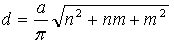
- CNTs are allotropes of carbon with a cylindrical nanostructure. These cylindrical carbon molecules have novel properties, making them useful in many applications in nanotechnology, electronics, optics and other fields of materials science. They exhibit extraordinary strength and unique electrical properties and are efficient thermal conductors.The band gap of carbon nanotube is directly affected by its chirality and diameter. If those properties can be controlled, CNTs would be the best candidate for nano-scale transistor devices.The way the graphene sheet is wrapped is represented by a pair of indices (n, m) called the chiral vector. The integers n and m denote the number of unit vectors along two directions in the “honey comb” crystal lattice of graphene. If m=0, the nanotubes are called zigzag. If n = m, the nanotubes are called armchair. Otherwise, they are called chiral (Martel et al., 2001).The diameter of a nanotube can be calculated from its (n, m) indices by using the expression of equation 1 below;
 | (1) |
4. Discussions
4.1. Nanosensor Architecture and Wireless Network
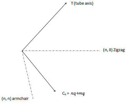
- A nanosensor network should be composed of a large number of nanosensor nodes that are densely deployed. Nanosensor nodes are scattered in a special domain called “sensor field”. Each of the distributed nodes equipped with a graphene-based nanoantenna typically has the capability to communicate with their neighbours, collect data, analyze them and route them to the designated sink point.Inorder to turn existing nanosensors into autonomous devices that can create a network, it is necessary to embed them with additional functionalities such as power source, processing capabilities and onboard storage. The sensing range of a single nanosensor is limited to its close environment. However, a wireless nanosensor network (WNSN) would be able to cover large areas, reach unprecedented locations in a non-invasive way and perform in-networking processing and cooperative actuation.A single nanosensor device, sensing or detecting a relevant event would communicate with its neighbours and transmit the information in a multi-hop (tree topology) fashion to a sink or command centre, which will connect with the macro-world and the final users. Furthermore, their communication capabilities would allow them to receive commands from other devices to either change behaviour or actuate, as the case may be. The components of a typical sensing node are shown in figure 2
4.2. Enhancement of Signals
- One of the essential attributes of a nanosensor is that it should be able to detect minute quantities of an analyte. However, at those atomic scales, the issue of signal enhancement should be addressed.The enhancement of signals may be done using frequency multipliers such as Gunn diodes, IMPATT (Impact Ionization Avalanche Transit-Time) diodes and Schottky diodes. The operation is based on the application of wave whose frequency is a fraction of the desired frequency to a non-linear circuit that distorts the input signal and consequently its harmonics are generated in the device. A subsequent band pass filter selects the desired harmonic frequency and removes the unwanted fundamental and other harmonics from the output. Figure 3 shows the block diagram for frequency multiplication.
4.3. Applications of Wireless Nanosensor Networks
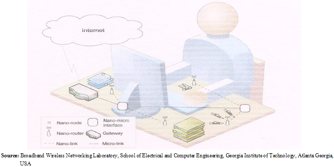
- The applications of wireless nanosensor networks (WNSNs) are broadly classified into environmental, medical, military and industrial.Environmental ApplicationsTraditionally, sensor networks are used in the context of high environmental applications such as radiation and nuclear threat detection systems, weather sensing, habitat sensing and seismic monitoring. Other potential applications include, microclimates, forest fire detection and flood detection. Chemical-physical-acoustic and image based sensors can be utilized to study ecosystems (example, in support of global parameters such as temperature and population of microorganisms) (Sohraby et al., 2007).However, the high sensibility and the large diversity of chemical nanosensors can be exploited in other environmental applications such as precision agriculture (plant monitoring and plagues defeating systems). Precision farming, also known as site-specific management describes a bundle of new Information Technologies applied to management of large-scale commercial agriculture. Precision farming relies upon intensive sensing of environmental conditions and Computer processing of resulting data to inform decision making and control farm machinery. This technology typically connects Global Positioning System (GPS) with satellite imaging of fields to remotely sense crop pests or evidence of drought and then automatically adjust levels of irrigation or pesticide application.If the network of Wireless Nanosensors function as designed, ubiquitous wireless sensors will become an essential tool for bringing this vision of precision farming to maturity.Medical ApplicationsBiological nanosensors provide an interface between biological phenomena and electronic nano-devices. Wireless nanosensor networks have potential application in Remote Monitoring of Physiological Data.Remote Monitoring of Physiological DataThe presence of different infectious agents in the body can be monitored by means of nanosensors. In addition, the level of cholesterol, sodium, glucose and other ions in the blood can be monitored. For example, tattoo-like sensors (fluorescent ion-selective nanosensors for intracellular analysis) can be used to monitor glucose level in blood, etc.Figure 4 shows different nanosensors distributed around the body, defining a human body nanosensor network that can be used to gather data about the level of different substances.A wireless interface between these nanosensors and a micro-device such as a cellphone or specialized medical equipment (gateway) could be used to collect all these data and forward them to the healthcare provider through the internet.Military ApplicationsSelf-organization ability and fault tolerant characteristics of WNSNs make them versatile for military applications such as:(1) Nuclear, biological and chemical attack detection(2) Battlefield surveillance: Monitoring of inimical and friendly forces.(3) Armour damage detection.(1) Nuclear, Biological and Chemical Attack DetectionChemical and biological nanosensors can be used to detect harmful chemical/biological weapons in a distributed manner. One of the main benefits of using nanosensors rather than classical chemical sensors is that the presence of a chemical composite can be detected in a concentration as low as one molecule. However, taking into account that these sensors need direct contact with the molecules, having a network with a very large number of nanosensor node is necessary. In addition, by means of chemical nanosensors, it is possible to recover the molecular composition of a battlefield without requiring external and large equipments such as devices used for spectroscopy. A WNSN will be able to convey the information of the molecular composition of the air in a specific location to a macro-device within a very short time.(2) Battle Field Surveillance: Monitoring Inimical and Friendly ForcesOn the battlefield, nanosensors can be used to identify and/or attract friendly or inimical objects, vehicles, aircraft and personnel (soldiers). Sensor nodes can be deployed on a battlefield, in front of or beyond enemy lines. Here, a system of networked nanosensors can detect and attract threats and be utilized for weapon targeting and area denial. Soldiers covered with nanosensors would submit data to remote servers where monitoring agents will be able to know the status of soldiers in the battlefield.(3) Armour Damage DetectionPhysical nanosensors can be used to detect very small cracks in textiles, civil structures (bridges, buildings), vehicles, etc. By having a network of nanosensors distributed over the structures that have to be monitored and by means of interaction with micro or macro devices, WNSNs can be used to detect, the origin of problems in functionalized soldiers’ armour and other structures exposed to attacks.Industrial and Commercial ApplicationsIndustrial and commercial applications include, but are not limited to, Future Interconnected Office (FIO) application.Future Interconnected OfficeThe interconnection of nanosensor and nano-actuator devices with existing communication networks and ultimately the internet enables new interesting applications that will influence how offices operate. For example, in an interconnected office, every single element can be permanently connected to the internet. As a result, a user can keep track of all professional belongings, as well as assets and liabilities management. Figure 5 illustrates the architecture for a future interconnected office.
5. Results
- Algorithm for nanosensor application using interpolation network 27.0.0.1 modelUsing the medical field as an example, a guide as to how the capabilities of a nanosensor senses a signal and communicates it to its neighbours located in a sensor field is illustrated using the algorithm below.001 Defines parameters = primary keys = VAR (A, B, C, D)002 Primary key parameters VAR (A) = DNA003 Primary key parameters VAR (B) = Enzymes004 Primary key parameters VAR (C) = Antibody005 Primary key parameters VAR (D) = Antigen006 Infuse defined parameters VAR (A, B, C, D) in an open source machine.007 Define an object = secondary parameter = VAR (H)008 Contact VAR (H) on the open source009 Enhance object on line 006010 If the object on line 006 = VAR (A) = DNA011 Repeat 009012 End 011013 Then Go to 017014 Else Go to 007015 End 014016 Repeat 009 until VAR (A, B, C, D) = [VAR (H)]; [VAR (B)]; [VAR (C)]; (VAR (D)]017 End 016; for VAR (A, B, C, D) = ([DNA; Enzymes; Antibody; Antigen])018 End 009A navigation on the intra-network system on mother nanosensor 27.0.0.1 unto 27.0.0.2, 27.0.0.3, etc displays the results of line 016 of the algorithm/Program on all the sensors within the defined area (Sensor field), with demonstrated simulation using computer systems.Nanosensor PC SimulatorNanosensor PC simulator is an application software designed to simulate the working process in a communication nanosensor network. The simulator has two components; PC Mother Sensor viewer that runs on the computer system that serves as the server and the Nanosensor PC that runs on the computer that serves as the host/node.The PC Mother sensor detects and displays the attributes of all Nanosensor PCs on a wireless network configured within the same IP range. If the Mother Sensor Viewer is running on 192.168.10.50, then all other computers on which the Nanosensor PC will run are configured with IP addresses within the range of 192.168.10.1 to 192.168.10.254, except 192.168.10.50 assigned to the Mother Sensor Viewer. This will establish a protocol that forms the basis for their communication.The Nanosensor PC is a component of the application that runs on any computer in a wireless environment. Whenever the Nanosensor PC runs, it displays its properties on its panel and waits for the Mother Sensor Viewer’s request. As soon as the Viewer requests for its properties, it sends them on any computer provided it is running the same application and on the same network.
 | Figure 1. The (n,m) nanotube-naming scheme thought of as a unit vector (Ch) in an infinite graphene sheet that describes how to “roll up” a graphene sheet to form nanotubes |
 | Figure 2. Typical nanosensor node (Zhang, 2004) |
 | Figure 3. Process of frequency multiplication for signal enhancement. Where ω0is the frequency to be multiplied, n ω0 is the number times, the frequency is multiplied |
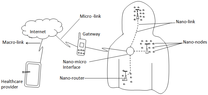 | Figure 4. Architecture for Wireless Nanosensor Networks in health application |
 | Figure 5. Architecture for a future interconnected office |
6. Conclusions
- Nanotechnology is enabling the development of devices in a scale ranging from one to a few hundred nanometres. One of the promising applications of this technology is in the field of sensing. A nanosensor is not only a tiny sensor, but also a device that makes use of novel properties of nanomaterials, especially carbon nanotubes (CNTs) to detect and measure new types of events in the nanoscale, employing carbon-based EM nanotransceivers and nanoantennas.However, the sensing range of a single nanosensor is limited to its close environment and thus many nanosensors are needed to create a network. The development of an integrated nanosensor device with communication capabilities will overcome the limitations of individual nanosensors and expand their potential applications.The working process of a Wireless Nanosensor Communication Network is illustrated using an interpolating algorithm to show how a Nanosensor node detects a signal. In addition, a Nanosensor PC Simulator was designed using JCreator LE Setup to demonstrate signal exchange in a WNSN.