-
Paper Information
- Next Paper
- Paper Submission
-
Journal Information
- About This Journal
- Editorial Board
- Current Issue
- Archive
- Author Guidelines
- Contact Us
International Journal of Materials Engineering
p-ISSN: 2166-5389 e-ISSN: 2166-5400
2013; 3(1): 1-3
doi:10.5923/j.ijme.20130301.01
Ohmic Contacts to P-Type Doped ZnO
 Abstract
 Reference
 Full-Text PDF
 Full-text HTML
L. S. Chuah1, S. S. Tneh2, Z. Hassan2, K. K. Saw1, F. F. Yam2
1Physics Section, School of Distance Education, Universiti Sains Malaysia, 11800 Penang, Malaysia
2School of Physics, Universiti Sains Malaysia, 11800 Penang, Malaysia
Correspondence to: L. S. Chuah, Physics Section, School of Distance Education, Universiti Sains Malaysia, 11800 Penang, Malaysia.
| Email: |  |
Copyright © 2012 Scientific & Academic Publishing. All Rights Reserved.
For the purpose of enhance the ohmic contacts, we have utilizing Pt to act as ohmic contacts on p-type phosphorus doped ZnO (ZnO:P) by a metal with high work function. The Pt ohmic contacts in terms of electrical property and thermal stability were reported in this paper. The ZnO films doped with 3 wt. % phosphorus (P) were produced by activating phosphorus doped ZnO (ZnO:P) thin films in air ambient at 300℃, 400℃, 500℃, and 600℃ for 60 min without any catalyst. The activation energies of the phosphorus dopant in the p-type ZnO under air environment show that phosphorus replacement on the O-site compliance a deep level in the gap.
Keywords: ZnO, Doping, Semiconducting II–VI Materials, Ohmic
Cite this paper: L. S. Chuah, S. S. Tneh, Z. Hassan, K. K. Saw, F. F. Yam, Ohmic Contacts to P-Type Doped ZnO, International Journal of Materials Engineering, Vol. 3 No. 1, 2013, pp. 1-3. doi: 10.5923/j.ijme.20130301.01.
1. Introduction
- Zinc oxide (ZnO), with a high exciton binding energy (60 meV) and a large band gap (3.37 eV at room temperature). ZnO is a material strong agreed to implementations in ultra-violet (UV) optoelectronic devices, for example light-emitting diodes (LEDs), laser diodes (LDs), field-effect transistors (FETs), and solar blind ultraviolet (UV) photo detectors[1]. In consequence, two categorization of p-type ohmic contact with high reflectivity and low specific contact resistance have been investigated to improve low resistance ohmic contacts to p-type GaN with light reflectance to perform high light extraction efficiency in flip chip light-emitting diodes (FCLEDs). The primary one is situated on the multilayer metal contact, such as Ir/Ag, Pd/Ni/Al/Ti/Au, Ni/Ag/Au and Ni/Au/Rh. The additional is founded on transparent conductive oxide contact (antireflection coating), such as MIO/Ag and ICO/Ag[2].Simultaneous discoveries in obtaining high quality p-type ZnO and comprehension of electroluminescence (EL) from ZnO based pn junctions confirm that practical utilizations of ZnO LEDs can be anticipate soon [3–7]. Nonetheless, devices with high contact resistance between the electrode metals and the semiconductors would greatly limit the performance. Consequently, fabrication of high quality ohmic contacts with low contact resistivity and high thermal stability is advantages for ZnO-based optoelectronic devices. Because of difficulty in growing high quality p-type conductivity ZnO, reports on ohmic contact to p-ZnO are only few. In those limited literatures, metal such as Ti/Au and Ni/Au were often chosen as ohmic contacts to p-type ZnO or p-ZnMgO due to their high work function[8,9]. But the earlier was found to be not so thermal stable, the morphology of which became rough even after annealing at temperatures up to 150℃[10]. While Ni/Au bilayer electrodes was used to form ohmic contacts to other p-type semiconductors, such as GaN and CuCrO2[11,12]. Lu et. al. provided an approach, in their study, ohmic contacts to N-doped p-type ZnO was studied[13, 14]. As a means to enhance the ohmic contacts, we have apply Pt to perform as ohmic contacts on p-type ZnO by choice of metal with needed high work function. In this paper, the Pt ohmic contacts in terms of electrical property and thermal stability were investigated.
2. Experiment
- The phosphorus (3 wt %) p-doped ZnO films of about 500 nm thickness were grown on glass substrates by the thermal evaporation technique. Subsequently, activating thin films by thermal oxidation in air without any catalysts. The oxidation was conducted at 300℃, 400℃, 500℃, 600℃ for 1 hours without any catalyst. The essential factor is that an oxygen-rich condition was raised to minimize the formation of zinc interstitials and oxygen vacancies. After the growth of ZnO:P films, a Pt (100 nm) contact metal layers were deposited sequentially by dc sputtering. Atomic force microscopy (AFM) was used to analyze surface morphology.The metal mask which was applied for ohmic contacts fabrication includes of an array of dots with diameter of 100 µm. Contact was formed on the top surface of the sample. The contact is characterized by Keithleyhigh-voltage-source-measure-unit (model 237) for its I-V characteristics.
3. Results and Discussion
- Fig. 1 shows the I–V characteristic of the fabricated Pt contacts. The sample annealed at 600℃ exhibited the best I–V characteristics of all samples. From the plots, we found that samples annealed at 400℃, 500℃, 600℃ were ohmic. The current conducted through the 300℃ was in mini-Ampere (mA). For 400℃, 500℃, 600℃ samples, the current increased visible reached nano-Ampere (nA) grade. The contacts at 500℃ annealing revealed the largest current conduction. Consequently, the contact resistance depends on the annealed temperature[15].AFM 3D analysis was performed to see the surface morphology of the ZnO:P thin films (see Fig. 2). The AFM image scale was 5 × 5 μm2. We have proved the small-grained, columnar structure of the ZnO:P thin film. The ZnO thin film diffused at 600℃ appeared to be composed of converging grains with increased surface roughness. Specifically, the surface roughnesses of the ZnO:P thin films were 11.23, 12.53, 16.70 and 19.21 nm, for 300℃, 400℃, 500℃, 600℃, respectively. The increased surface roughness after diffusion is due to recrystallization of the crystalline structure.
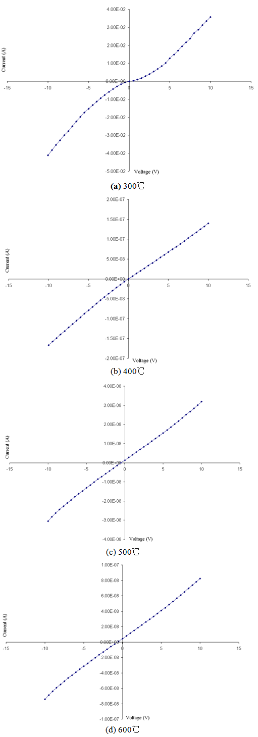 | Figure 1. The I–V characteristics of Pt/ZnO:P deposited on glass |
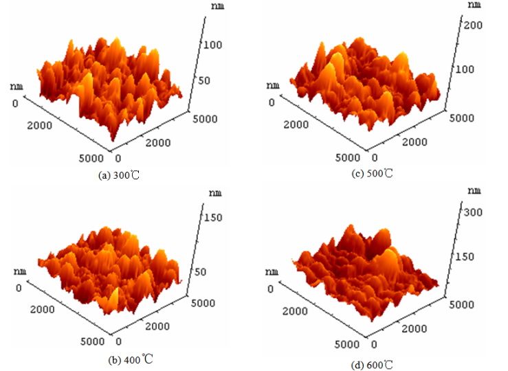 | Figure 2. AFM 3D images of the Pt/ZnO:P deposited on glass |
4. Conclusions
- ZnO:P films were prepared by annealing film in air at temperatures from 300 to 600℃. The sample annealed at 600 ℃ exhibited the best I–V characteristics of all samples. From the plots, we found that samples annealed at 400℃, 500℃, 600℃ were ohmic. The current conducted through the 300℃ was in mini-Ampere (mA). For 400℃, 500℃, 600℃ samples, the current increased visible reached nano-Ampere (nA) grade. The AFM image scale was 5 × 5 μm2. We confirmed the small-grained, columnar structure of the ZnO:P thin film. The ZnO:P thin film at 600℃ appeared to be composed of converging grains with increased surface roughness. Specifically, the surface roughnesses of the ZnO:P thin films were 11.23, 12.53, 16.70 and 19.21 nm, for 300℃, 400℃, 500℃, 600℃, respectively.
ACKNOWLEDGEMENTS
- The support from Universiti Sains Malaysia and FRGS (203/PJJAUH/6711159) are gratefully acknowledged.