-
Paper Information
- Next Paper
- Previous Paper
- Paper Submission
-
Journal Information
- About This Journal
- Editorial Board
- Current Issue
- Archive
- Author Guidelines
- Contact Us
International Journal of Materials Engineering
p-ISSN: 2166-5389 e-ISSN: 2166-5400
2012; 2(3): 17-22
doi: 10.5923/j.ijme.20120203.02
Possible Realization of Near Optimum Efficiency from n-Si-Ge/p-Ge-Si DDR Hetero Structure IMPATT Diode
 Abstract
 Reference
 Full-Text PDF
 Full-Text HTML
P. R. Tripathy1, M. Mukherjee2, S. P. Pati3
1Department of Electronics and Telecommunication Engineering, Purushottam Institute of Engineering and Technology, Rourkela, Odisha, 770034, India
2CMSDS, Institute of Radio Physics and Electronics, Calcutta University, Kolkata, 700009, India
3National Institute of Science and Technology, Pelur Hills, Berhampur, Odisha, India
Correspondence to: P. R. Tripathy, Department of Electronics and Telecommunication Engineering, Purushottam Institute of Engineering and Technology, Rourkela, Odisha, 770034, India.
| Email: |  |
Copyright © 2012 Scientific & Academic Publishing. All Rights Reserved.
Avalanche breakdown in a p-n junction can generate rf negative resistance due to twin delay mechanism (Avalanche Delay associated with growth of charge bump and transit time delay caused due to time elapsed for the grown charge bump drifting through the depletion zone) leading to generation of high frequency power in IMPATT mode. With the advancement of device technology and with the motive of furtherance of device performance, replacement of homo junction of single elemental semiconductor with hetero junction, hetero structure junctions from lattice matched pair of elemental semiconductors is now being explored as supported by recent reports. The introduction of an n-Ge and p-Ge impurity bumps on either side of junction interface of a Si p-n junction, results in the formation of a n-Si-Ge/p-Ge-Si hetero structure p-n junction. The analysis of such hetero structure Impatt diode for generation of micro/mm-wave power at designed atmospheric window frequencies of 15 and 94 GHz becomes the scope of the study of this paper. The results are computed through three tier sophisticated computer algorithm indicate efficiency enhancement in case of proposed hetero structure to nearly 29% (at X-band) as against only 14% for the corresponding the homo junction diodes associated with increase of diode negative conductance by nearly two fold which in turn could enhance the rf power delivery from the hetero structure diode by many fold. Presence of low BG Ge near high field junction interface and its order high carrier ionization rate (compared to Si) localizes the avalanche zone to below 10% of the depletion zone and thereby pushes the device efficiency and value of negative conductance. However the performance of complementary n-Ge-Si/p-Si-Ge hetero structure remains close to Si or Ge homo junction. The results are highly encouraging which may make Si-Ge-Si Hetero Structure Diode as a prospective microwave generator.
Keywords: Hetero Structure, DDR, Germanium, Impact Ionization, RF Power, Silicon
Article Outline
1. Introduction
- Impatt (Impact Avalanche Transit Time) device is a class of rf negative resistance power generator which can cover frequencies from X-band to sub-mm-wave band (10-5000 GHz). Any form of junction fabricated from any semiconductor can operate in Impatt mode. Advance research work is being carried out round the globe with the objective of realizing high power at high efficiency and with low noise even at mm- and sub-mm-wave frequencies[1]. With the advancement of device technology and with the motive of furtherance of device rf performance, possible replacement of homo junction of single elemental semiconductor with hetero junction or hetero structure junctions from lattice matched pair of elemental semiconductors is being explored as supported by recent reports[2-6]. Si and Ge are twoconventional group IV semiconductors having tolerable lattice mismatch. Homo junctions from Si and Ge have become a reality in producing Impatt Power since decades. Hetero junctions from Si and Ge for other purposes have already been reported[7]. The authors have studied a new form of junction in the form of n-Si-Ge/p-Ge-Si hetero structure junction when both the p- and n- layers contain two materials. The band gap of Ge is 0.66 eV where as for Si, it is 1.12 eV. The carrier ionization rate causing avalanche breakdown remains high for low BG semiconductors. In fact the carrier ionization rate for Ge is higher by an order of magnitude compared to that for Si at the same magnitude of electric field. The order gap in values of carrier ionization rate between Ge and Si further widens if Ge is placed in high field zone close to junction and Si placed away from junction. With this idea in mind, the authors proposed Si-Ge-Si hetero structure junction of the form n-Si-Ge/p-Ge-Si when Ge impurity bumps are introduced near the junction interface on either sides of conventional Si homo junction leading to above referred hetero structure junction. The high values of electron and hole ionization rate of Ge in the high field zone near junction plane, thins the avalanche zone to less than 10% (3% in X-band) of the depletion zone on either side of the junction. This phenomenon makes this structure creditable as both the efficiency and diode negative conductance would be pushed to sufficiently high values as compared to both Si and Ge homo junctions. The authors have analysed the new diode structure following a sophisticated three tier computer algorithm. The diode has been designed and optimized for atmospheric window frequencies in X-band (15 GHz) and mm-wave band (94 GHz). The results observed are quite interesting indicating this device to be promising candidate for high power generation with high efficiency. The efficiency of this new proposed diode mounts to near optimum value of 29% for the X-band hetero structure diode as against 12-14% for homo junctions together with the diode negative conductance being doubled for the hetero structure. These characteristics would help in pushing the rf power delivery from the diode. Further, since the avalanching process is augmented and ionizing layer thinned down drastically, the avalanche noise from the hetero structure may remain quite low.
2. Computer Simulation Method
- The typical general Impatt diode structure is shown in figure 1 for both the frequencies of design. The minority carriers say holes, under the influence of reverse breakdown voltage (field) crosses from n side to p side, passing through the high field zone around the junction. The hole charge concentration grows due to impact avalanche ionization process, thereby the reverse saturation hole current Jps at n side edge grows to Jp on the p side extreme. Similarly the minority electron moves from p-side to n-side growing from Jns to Jn. The charge growth up to the extent of 95%, takes place within the avalanche region (xA). Then the grown charge drifts through drift region (holes in dp) and (electrons in dn) with respective saturated carrier drift velocity.
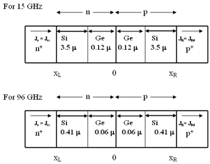 | Figure 1. Schematic diagram of typical double drift n-Si-Ge/p-Ge-Si- based Impatt diode p-n Junction at 15.0 and 96.0 GHz |
2.1. Analysis under Static Conditions
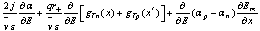
- Two separate realistic self-converging iterative computer simulation programs have been framed for DC analysis and small signal analyses. Material parameters like the ionization rate, drift velocities etc., of all the materials have been taken from the recently reported published literature[8-10]. The diode active layer width is divided into large number of space steps of 1 nm per micron or less. The DC analysis is carried out by solving simultaneously three non-linear device equations namely Poisson’s equation, the carrier continuity equation and the space charge equation using a double iterative field maximum initiated simulation program[7] subject to fulfilment of boundary conditions in electric field and carrier currents[11].The basic equations for DC analysis are,Poisson’s equation,
 | (1) |
 | (2) |
 | (3) |
 | (4) |
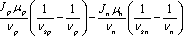 is regarded as correction factor and can be evaluated from velocity ~ field characteristics in any semiconductor. The equations (1), (2) and (4), which consider only drift current, can be modified to incorporate diffusion and tunnel currents[12]. The dc analysis gives drift voltage drop (VD), normalized avalanche zone (xA/W), breakdown electric field and voltage (Em & VB), qualitative value of device efficiency (η) etc.[13]. The edges of the depletion zone are also determined accurately from this analysis. The DC electric field profiles, carrier current profiles, breakdown voltage etc. are obtained from this analysis. We have considered a one-dimensional model with doping distributions of the form n+npp+. The data obtained from the DC analysis are used as input for the high frequency analysis of the diode. The next phase of the computation has been designed for computation of RF properties of the optimized diodes over a wide band of frequencies. Implicit second order device equations on diode resistance and susceptance are framed based on Gummel-Blue approach[14].
2.2. High Frequency Analysis
- The ac model takes into account the contribution of negative resistance from each space point and effectively determines the device performance parameters such as negative conductance (-G), susceptance (B) and negative resistance (-ZR) of the diode. The variations of these values with frequency are also computed with the help of another double iterative computer program[15]. In the high frequency analysis, it is possible to find out the spatial variation of negative resistance (R) and reactance (X) in the depletion layer which would provide a clear idea regarding intensity of microwave oscillation produced along different region of the diode. The unperturbed diode impedance Z0 (without considering diffusion current) is separated into its real and imaginary components (i.e. Z0 = R0+iX0) to obtain the second order non-linear implicit differential equation in small signal resistance (R0) and reactance (X0) as,
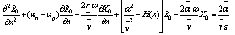 | (5) |
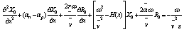 | (6) |
 The equations (5) and (6) are solved simultaneously by modified Runge-Kutta method[16]. Finally the small signal diode resistance (R) and reactance (X) due to drift, diffusion and tunnel currents are obtained from the expression including perturbation part,
 and
and  The integrated values of resistance and reactance give ZR and ZX using the relation,
 and
and  Using the values of ZR and ZX, the diode conductance (G), susceptance (B) and the quality factor (Q) are calculated using the relation
 and
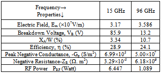
and  The series positive resistance (RS) of the device, which is one of the important limiting factors responsible for limiting power output and device efficiency, can also is determined. The RF power is estimated from the following[17]:
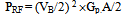 | (7) |
3. Computer Algorithm for DC and RF Analysis
- Computer solutions become essential for understanding the properties of the devices, as analytical methods are not feasible to provide accurate information regarding the DC and high frequency parameters of these devices as the equations are complicated.
3.1. DC Computer Method
- First the value of the field maximum E0 and its location x0 are suitably chosen for the diode. Then the Poisson’s equation and the carrier continuity equations are solved simultaneously through numerical approach. The space step width is taken to be very small i.e. of the order of nms (1000 steps per micron). The numerical solution is progressed from the point x=x0 and moving first towards the right side and then towards left hand side of the field maximum till the field/carrier current boundary conditions are satisfied at x=xR,L. A four track rapidly converging logic is framed to get the boundary condition satisfied at the edges of the depletion layer. The breakdown characteristics, efficiency are thus obtained from final solution[7].
3.2. RF Analysis
|
4. Results and Discussions
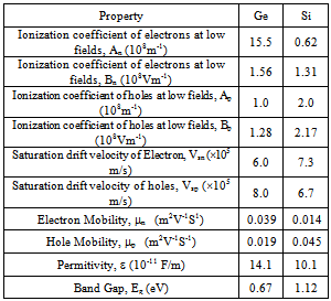
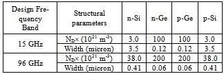
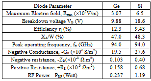
- Si/Ge hetero diode structure having the form n-Si- Ge/p-Ge-Si has been designed and optimized for frequencies of operation around 15 and 96 GHz. The materials parameters of both the materials are taken from recent experimental reports[8-10] are shown in Table 1. The electron/hole ionization rate (α, β) are obtained using exponential equations of the form, α, β = An,pexp(bn,p/E)m, m=1.0 for Si and GeThe structural and design parameter for the diode are presented in table 2. The realistic doping profile across the junction is considered through use of an appropriate exponential function. A thin and highly doped Ge layer of width 120 nm and doping, 1×10²³/m3, (as compared to Si layer, width= 3.5 micron, doping= 3×10²¹/m3) is considered near the junction plane. The presence of highly doped Ge layer pushes the breakdown electric field maximum value (3.17×10⁷ V/m).
|
|
|
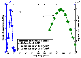 | Figure 2. Frequency Vs Negative Conductance for the IMPATT Diode (n-Si-Ge/p-Ge-Si) at both 15 and 96 GHz Peak Frequency |
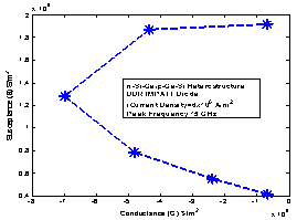 | Figure 3. Admittance plot of n-Si-Ge/p-Ge-Si DDR (n+npp+) IMPATT diode (Peak frequency= 15 GHz) |
 | Figure 4. Admittance plot of n-Si-Ge/p-Ge-Si DDR (n+npp+) IMPATT diode (Peak frequency= 96 GHz) |
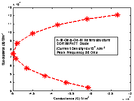
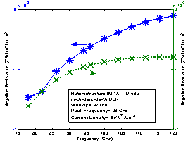 | Figure 5. Plots of the variation of impedance of DDR Hetero structure Impatt diode |
5. Conclusions
- Thus the hetero structure diode of the form n-Si-Ge/p-Ge-Si would provide the best rf performance amongst above cited the homo junction diodes and complementary hetero structure diode.
ACKNOWLEDGEMENTs
- Prof. S. P. Pati wishes to express his sincere thanks to AICTE, New Delhi for grant of Emeritus Fellowship in his favour.