-
Paper Information
- Previous Paper
- Paper Submission
-
Journal Information
- About This Journal
- Editorial Board
- Current Issue
- Archive
- Author Guidelines
- Contact Us
International Journal of Materials Engineering
p-ISSN: 2166-5389 e-ISSN: 2166-5400
2012; 2(1): 12-17
doi:10.5923/j.ijme.20120201.03
Studies on Structural, Optical and Electrical Properties of ZnO Thin Films Prepared by the Spray Pyrolysis Method
 Abstract
 Reference
 Full-Text PDF
 Full-text HTML
L. C. Nehru1, M. Umadevi1, C. Sanjeeviraja2
1Department of Physics, Mother Teresa Women’s University, Kodaikanal, 624102, India
2School of Physics, Alagappa University, Karaikudi, 630002, India
Correspondence to: C. Sanjeeviraja, School of Physics, Alagappa University, Karaikudi, 630002, India.
| Email: |  |
Copyright © 2012 Scientific & Academic Publishing. All Rights Reserved.
Zinc oxide transparent thin films have been deposited on glass substrates by a pneumatic spray pyrolysis technique. Surface investigations such as AFM, SEM and XRD patterns of the films were investigated for as-deposited and annealed in air atmosphere. The morphology of the films is strongly related to the annealing temperature. By XRD, the amorphous phase is identified for as-deposited films and it changes to polycrystalline with the (1 0 0) and (1 0 1) as preferential crystallographic orientation for annealed samples. The as-deposited films exhibited highest optical transmittance and the direct band gap energy was found to vary from 3.23 to 3.07 eV with annealing temperatures. The electrical parameters of the samples were obtained by applying the dc four-probe technique. The effects of annealing environment on the luminescence characteristics of ZnO thin films were investigated by PL films are described here.
Keywords: ZnO, Thin film, Spray pyrolysis, Annealing temperature
Cite this paper: L. C. Nehru, M. Umadevi, C. Sanjeeviraja, Studies on Structural, Optical and Electrical Properties of ZnO Thin Films Prepared by the Spray Pyrolysis Method, International Journal of Materials Engineering , Vol. 2 No. 1, 2012, pp. 12-17. doi: 10.5923/j.ijme.20120201.03.
Article Outline
1. Introduction
- Transparent conductive oxide (TCO) consists of a degenerated wide band-gap semiconductor with low electrical resistivity and high transparency in the visible and near infrared wavelength range. A transparent conductive thin films including indium tin oxide (ITO) have many applications such as transparent electrodes, window materials in solar cell, light emitting diodes, flat panel displays and sensors[1-5]. However, high cost of ITO has motivated efforts to develop substitutes. Recently, zinc oxide (ZnO) with a hexagonal wurzite structure is a promising material to replace ITO in the above applications. It has a great interest in wide band gap semiconductors, because of the ever-increasing commercial desire for short wavelength light emitting devices. As a good candidate, ZnO-nanostructured films have wideband-gap (3.37 eV) and extremely large exciton binding energy of 60mV[6] at room temperature (RT), that provides more efficient excitonic lasing mechanism at RT. The efficiency and performance of any optical and electrical nanodevices are directly determined by the properties of underlying nanostructures, which are in turn greatly dependent on the crystallographic orientation, size, shape, and morphology. A highly transparent ZnO films have been prepared by many different deposition techniques and their corresponding deposition parameters play an important role in controlling the morphology and physical properties of the nanostructures. Both physical deposition, including thermal evaporation, sputtering, spray pyrolysis, metal organic chemical vapor deposition (MOCVD), pulsed laser deposition, molecular beam epitaxy (MBE) [7-15], and chemical synthetic routes, including hydrothermal, solvo-thermal, sol–gel, electrochemical, chemical bath deposition [16-26] have been successfully employed to prepare a wide variety of ZnO nanostructures. The physical deposition routes have the advantages of producing high-quality materials, but also the disadvantage of the need for high temperature.Spray pyrolysis technology is a convenient for the deposition of semiconductor thin films and has the several advantages in comparison with other deposition techniques such as low cost of the source materials, producing high- quality films using comparatively simple deposition equipment, moderate substrate temperatures, deposition scaled for large area and uniform deposition with very thin layers with specific composition, morphology, good adhesion between the deposited film and controlling the shape and sizes. The morphology of the material depends on the thermal treatment. Usually, as-deposited films require a thermal treatment to improve stability and reduce the possible undesirable influence of the substrate. It has been reported previously that high-purity crystalline ZnO thin films can be fabricated by spray pyrolysis. The key success of spray pyrolysis is using a single-solid organic zinc fountain as a precursor with the physical and chemical properties required depositing a pure film at the substrate. Thermal annealing is a widely used method to improve crystal quality and to study structural defects in materials. During an annealing process, dislocations and other structural defects will move in the material and adsorption/decomposition will occur on the surface, thus the structure and the stoichiometric ratio of the material will change. Such phenomena can have major effects on semiconductor device properties, light emitting devices being particularly affected. For ZnO films, many research groups have investigated the effects of annealing temperatures (Ta) on the structure and luminescence properties of ZnO films[27,28]. In this paper, we report the preliminary results on the growth of ZnO thin films on glass substrates using hydrated zinc acetate [Zn (CH3COO)2.4H2O] as precursor in ethanol with tri-ethylene glycol (TEG). The aim of the present study is to investigate the general features of the annealing effect of the prepared ZnO thin films. Then, the films were characterized to examine the structural, electrical, optical and morphological properties are reported.
2. Experimental
- Chemical spray pyrolysis is one of the major techniques used to deposit a wide variety of materials including metal or alloy oxides. Generally, spray pyrolysis deposition system which is mainly consists of the following four sections: (a) the reactants and carrier gas assembly connected to the spray nozzle at the entrance of the reaction chamber, (b) the reaction chamber in which there is a resistive heater used to heat the substrate to the required temperature for thin film deposition, (c) the temperature controller that monitors the deposition temperature and controls the desired substrate temperature and (d) the exhausting gas module. The substrate temperature was measured using a K-type thermocouple to an accuracy of ± 1 K. This particular deposition technique involves the spraying of a fine mist of reactants onto planar hot substrates from a predetermined distance. Reactant droplets ending up in the substrates can undergo several phases, for example evaporation, solute condensation and thermal decomposition of volatile byproducts, which result in film formation. In the present work, ZnO films were prepared on corning microscope glass (of 1 cm2 geometric area) substrates using metal-organic zinc acetate di hydrate (Merck; > 99%) precursor in air atmosphere at a fixed substrate temperature of 300ºC. The spray solution was prepared by dissolving amounts of zinc acetate for predefined molarity in the solvent containing 80% of ethanol, 10% of hydrochloric acid and 10% of tri-ethylene glycol (TEG) were mixed directly well by vigorous magnetic stirring for 1 h. Ethanol has a very low boiling point (~ 80℃) and therefore, high substrate temperature causes the spray solution cone to partially evaporate even before they hit the substrate. This makes the surface morphology of the deposited films highly uneven and powdery. In order to prevent these undesired morphologies, TEG is added, which has a high boiling point (~280℃). Addition of TEG reduces both premature evaporation of the solvent in the spray cone while in transit from the spray nozzle to the substrate and the resultant loss of material during the condensation due to the substrate temperature. The spraying solution is always buffered by a small amount of HCl to increase the solubility and prevent precipitation in the solution. In this technique, substrate cleaning plays an important role in the deposition of thin films. First, commercially available microscope glass were boiled in chromic acid for 2 h, washed with detergent, rinsed three times in acetone and finally ultrasonically cleaned with distilled water before use. Each rinse for fifteen minutes; and then rinsed in ethanol for fifteen minutes they were put into the deposition chamber. The spray flow rate was fixed at about 0.3 ml min−1, and the distance between the spray gun nozzle and the substrate was placed parallel to the target surface with a 20 cm. The flow rate used and the spraying distance were optimized via several additional pre-tests for the best continuity of the films. In the present experiment, the heater block temperature is considered as the substrate temperature, which was kept at 300℃, and the deposited time was 10 min. The temperature of the substrates was fixed at a constant temperature and the temperature was measured by a standard K-type thermocouple. After spray pyrolysing, as-deposited ZnO thin films were removed from the spray pyrolysing chamber and were immediately rapid thermal annealing at tube furnace at various temperatures were increased from 350℃ to 450℃. The heating rate was 6℃/s and the dwell time was 1 h. After annealing, the samples were taken out for characterization. The thicknesses of the deposited films were in the range of 0.96 μm. The Phase purity and the crystallinity of the films was characterized by X-ray diffraction (XRD) using a ‘X’ Pert PRO PANalytical system with Ni filtered Cu Kα irradiation (λ = 1.5460 Å, 30 kV and 40 mA). The surface morphology was characterized using a Dimension-3000 atomic force microscope (AFM), the cross-sectional morphology being evaluated with a Hitachi S-4500 scanning electron microscope (SEM). The samples for SEM imaging were coated with a thin layer of gold film to avoid charging. The optical transmission spectra of the films were measured at room temperature in air using a double beam spectrophotometer (Hitachi) in the wavelength range of 300 to 900 nm. The photoluminescence (PL) characteristics of ZnO films were investigated by making photoluminescence measurements using a Varian model Cary Eclipse fluorescence spectrophotometer. A 15W Xenon pulse lamp with a wavelength of 320 nm is used as the excitation light source, was used to evaluate the optical properties of the ZnO films. The electrical resistivity (or resistance) were characterized via Hall Effect measurements (Bio—Rad, HL5500PC) were carried out in a four-point Van der Pauw configuration with indium ohmic electrodes at room temperature. All the measurements were carried out at room temperature.
3. Results and Discussion
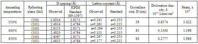
- The XRD patterns of the spray pyrolysis coated as- deposited ZnO and annealed ZnO films are shown in Fig. 1. The intensity data were collected over a range 2θ is 20 to 80º. Figs show the plots of intensity (in arbitrary unit) against 2θ. The result indicates that the films have a polycrystalline hexagonal wurtzite structure with (1 0 0) and (1 0 1) orientation. In Fig. 1(a) pattern shows that it was an amorphous phases for the as-deposited ZnO film. As the film was annealed at various temperatures the XRD pattern of ZnO at 350℃ (Fig. 1 (b)) shows very weak (1 0 0) and (1 0 1) diffraction peaks. Fig. 1(c) shows a strong X-ray peak from (1 0 0) planes with a weak (1 0 1) peak at 400℃. As the annealed temperature was increased further to 450℃, the intensity of the (1 0 0) peak in pattern (d) decreased in comparing with the pattern Fig. 1 (c), but (1 0 1) peak did not change. The (1 0 0) peak intensity is increased and then decreased with increasing temperature over the selected annealing temperature. The average sizes of crystallites (D) were calculated from the full width at half maximum (FWHM) of the diffraction peaks from the (1 0 0) and (1 0 1) planes of the films with the help of Scherrer formula[29]. The average crystallite size is 39, 85 and 60 nm were calculated for the annealed ZnO thin films, respectively.
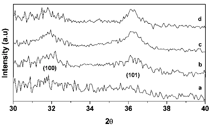 | Figure 1. XRD pattern of (a) as-deposited; (b) annealed at 350℃; (c) 400℃ and (d) 450℃ |
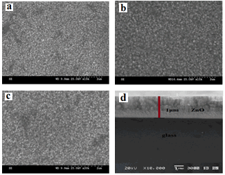 | Figure 2. SEM images of ZnO films (a) as-deposited; (b) annealed at 400℃; (c) annealed at 450℃ and (d) cross-sectional SEM morphology of sample film c in Fig. 1 |
|
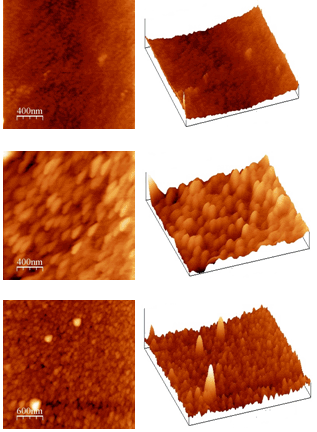 | Figure 3. AFM images of as-deposited and annealed sample film c and d in Fig. 1 |
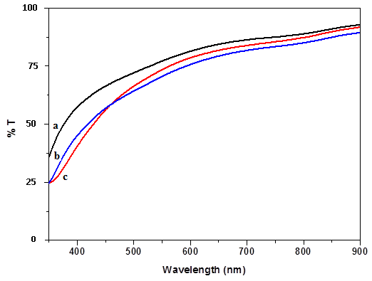 | Figure 4. Transmittance spectra of ZnO thin films prepared at different annealed temperature: (a) as-deposited; (b) 400℃ and (c) 450℃ |
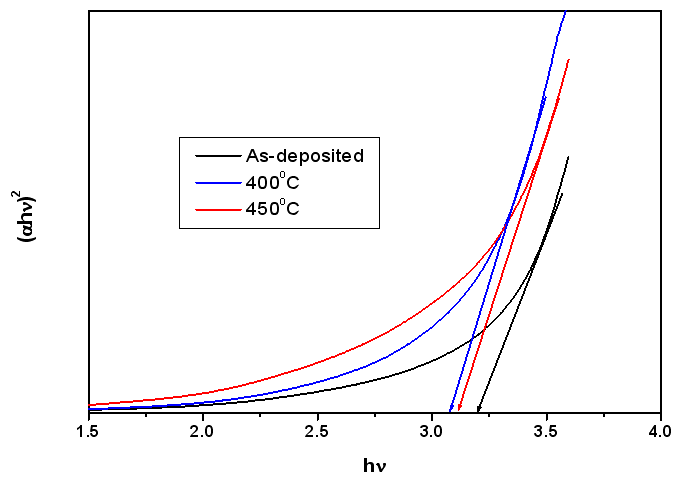 | Figure 5. Band gap variation as a function of annealing temperature |
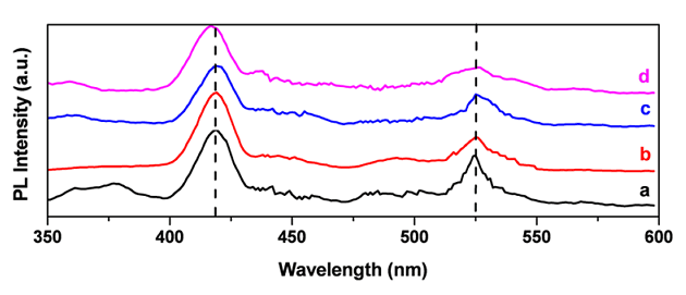 | Figure 6. PL spectra of ZnO films (a) as-deposited; (b) annealed at 350℃; (c) 400℃ and (d) 450℃ |
5. Conclusions
- Zinc oxide films have been successfully prepared on glass substrates using the spray pyrolysis technique. The process parameters were optimized to have good quality crystalline films. The films were optically clear, adherent and uniform. XRD characterization of the annealing films revealed polycrystalline. AFM studies confirmed the uniformity and well grown crystalline morphology of the ZnO films. The effect of annealing temperatures on electrical and optical properties of the films was studied. A highest resistivity of ~2.7x10⁻³ Ωcm is obtained for the as-deposited ZnO film sample. All the films were transparent in the visible region; with an average optical transmittance of 80%. The mechanism of violet and green luminescence emission from ZnO thin films annealed at various temperatures was investigated.
ACKNOWLEDGEMENTS
- One of the authors, L. C. Nehru would like to thank DST-CURIE Program, India for the financial support under Research Associate to carry out this research work at Department of Physics, Mother Teresa Women’s University, Kodaikanal-624 102, India