International Journal of Materials and Chemistry

p-ISSN: 2166-5346    e-ISSN: 2166-5354

2018;  8(1): 10-14

doi:10.5923/j.ijmc.20180801.02


A Study of the Absorption Edge of CdS:In Thin Films Prepared by the Spray Pyrolysis Technique

Shadia J. Ikhmayies

Al Isra University, Faculty of Information Technology, Department of Basic Sciences-Physics, Amman, Jordan

Correspondence to: Shadia J. Ikhmayies, Al Isra University, Faculty of Information Technology, Department of Basic Sciences-Physics, Amman, Jordan.

Email:

Copyright © 2018 Scientific & Academic Publishing. All Rights Reserved.

This work is licensed under the Creative Commons Attribution International License (CC BY).
http://creativecommons.org/licenses/by/4.0/

Abstract

Cadmium sulphide (CdS) is a II-VI compound with a wide band gap energy that enables it to be used as a window material in the CdTe based solar cells. In this work the absorption edge of indium doped cadmium sulphide (CdS:In) thin films was investigated. The films were prepared on glass substrates using the spray pyrolysis technique at a substrate temperature Ts = 490°C. X-ray diffraction (XRD) and scanning electron microscopy (SEM) revealed that the films are polycrystalline. The films displayed a wurtzite hexagonal structure with some indications of the presence of the cubic zinc blind phase. The transmittance of the films was measured at room temperature in the wavelength range 400–1100 nm and used to deduce the absorbance. The second derivative of the absorbance revealed the existence of the free exciton peaks of the wurtzite phase. The A and B free exciton peaks showed a merged peak and the C free exciton peak was apparent. These results were compared with those obtained by different authors. The separations of the aforementioned peaks were deduced and found to be in good agreement with the values found in the literature.

Keywords: Cadmium sulphide, Thin films, X-ray diffraction, Absorption edge, Exciton peaks, Heterojunction solar cells

Cite this paper: Shadia J. Ikhmayies, A Study of the Absorption Edge of CdS:In Thin Films Prepared by the Spray Pyrolysis Technique, International Journal of Materials and Chemistry, Vol. 8 No. 1, 2018, pp. 10-14. doi: 10.5923/j.ijmc.20180801.02.

1. Introduction

Cadmium sulphide CdS is a wide band gap II-VI compound semiconductor. It has direct band gaps (Eg) of 2.57 and 2.40 eV, at room temperature for hexagonal and cubic structures respectively [1]. CdS films have a great application potential such as the use in optoelectronic devices and solar cells [2, 3]. CdS is used as heterojunction partner for polycrystalline CdTe to fabricate CdTe/CdS solar cells, where a CdS layer is used as the n-type window layer [3]. To take advantage of the optoelectronic properties of CdS by producing n-type films, extrinsic doping is required. Several methods have been developed to grow n-type CdS films: for example; the variation of the reagent precursors concentration in order to vary the Cd:S ratio, or the doping with silver [4], chlorine [5] or indium atoms [6-9]. In this work indium was used as a dopant to produce n-type CdS thin films.
There are different techniques that can be used to obtain CdS thin films, such as rf sputtering [10], close spaced vapor transport (CSVT) [11], chemical bath deposition (CBD) [3, 12], close-spaced sublimation (CSS) [12], pulsed laser deposition (PLD) [13, 14], and spray pyrolysis (SP) [15-33]. However, the SP technique is a very low cost and simple technique that enables intentional doping and getting large area and uniform thin films.
In this work, the valence-band splitting of the wurtzite CdS:In thin films arising from the crystal field could be observed in the second derivative of the absorbance in the region of the absorption edge. The maxima related to the free exciton peaks of the wurtzite structure of CdS:In thin films were apparent and their positions and separations were deduced and compared with those obtained by other authors.

2. Experimental Procedure

The films were prepared by the spray pyrolysis (SP) technique on glass substrates as described elsewhere [15-19]. The dimensions of the slides are (6cm × 2.6 cm × 0.1 cm) and the substrate temperature is 490°C. Approximately a stoichiometric solution of thiourea ((NH2)2CS) and cadmium chloride (CdCl2.H2O) in distilled water was used. Indium chloride (InCl3) was used as the source of indium, where the ratio of the concentration of indium ions to that of cadmium ions ([In]/[Cd]) in the sprayed solution was 10-2.
X-ray measurements were recorded by a Philips PW1840 Compact X-ray diffractometer system with Cu Kα (λ = 1.5405 Å). Both of the SEM micrographs and compositional analysis were taken by a FEI scanning electron microscope (Inspect F 50), which is supplied by X-ray energy dispersive spectroscopy (EDS) apparatus.
Transmittance of the films was measured by using a double beam Shimadzu UV 1601 (PC) spectrophotometer with respect to a piece of glass similar to the substrates in the wavelength range 400-1100 nm. The thickness of the films was estimated by using the transmission spectra of the films and Lambert law of absorption in a semiconductor.

3. Results and Discussion

Fig.1 shows the X-ray diffractogram (XRD) of one of CdS:In thin films prepared in this work. As seen in the figure the film is polycrystalline and it displays a predominantly wurtzite hexagonal structure. Weak lines of the zinc-blind phase can be observed such as C(2 2 0) and C(1 1 1) which overlaps with the (0 0 2) line of the hexagonal phase and the line C(3 1 1) which also overlaps with the H(1 1 2) of the hexagonal phase.
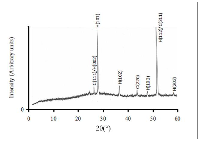
Figure 1. XRD diffractogram of one of the CdS:In thin films prepared by the SP technique
Fig.2 displays the SEM micrograph of one of the as-deposited CdS:In thin films under study. The mixed phase can be noticed through the deformed hexagonal and cubic shapes of grains in the SEM micrograph. The grain size is approximately in the range 0.1-0.5 µm.
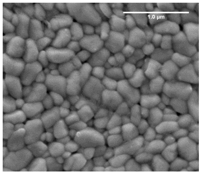
Figure 2. SEM image of one of the CdS:In thin films prepared by the SP technique
The composition of the films was explored using x-ray energy disspersive spectroscopy (EDS), and Fig.3 displays the EDS spectrum of one of the films. From the EDS report it is found that the ratios of Cd: S in the film is 51.05: 46.98 at.%, or 1.09. This means that the films are Cd rich, which is favoured for the use of the films as window layer in CdS/CdTe thin film solar cells, because this improves the n-type conductivity of the films. The ratio of In: Cd in the film is 1.97: 51.05, or 3.86%. Indium doping of the films is necessary to improve their n-type conductivity, where In replaces Cd, and it increases the number of free charge carriers.
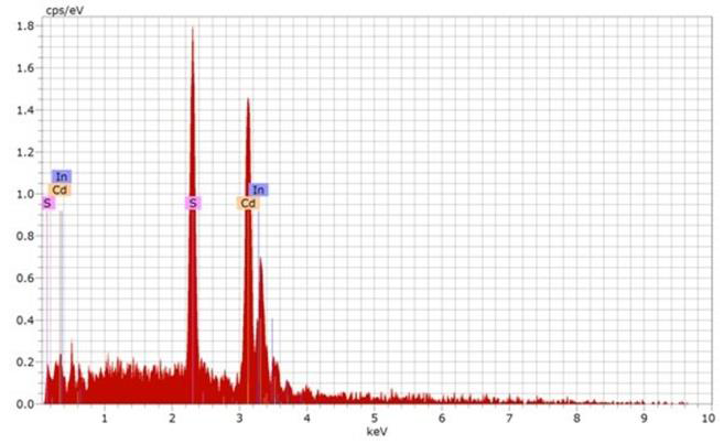
Figure 3. EDS spectrum of one of the CdS:In thin films prepared by the SP technique
The transmittance of the films was measured at room temperature in the wavelength range 400-1100 nm and used to deduce the absorbance. Fig.4 shows the absorbance of four CdS:In thin films of different thickness in the range 180-800 nm. As the figure shows the absorbance increases with film thickness in the high energy side after the absorption edge. The reason of this increase is the increase in the number of free charge carriers (electrons in this case). It is noticed that the absorption edge shifts towards lower energy with film thickness too. This shift is related to the increase in grain size with film thickness and hence the gradual disappearance of the quantum size effect. The sharpest absorption edge in the figure is that of the film of greatest thickness (800 nm) where the quantum size effect is the smallest. The absorption edge of the film of thickness 430 nm is the shallowest one in the figure. In the discussion of the second derivative of the absorbance of this film, evidence will be given that the growth of wurtzite and cubic phases is in an early stage in this film, and hence the crystallites have small sizes such that quantum size effect is effective.
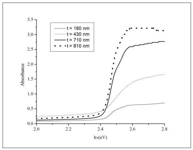
Figure 4. Absorbance of CdS:In thin films of different thickness against the photon's energy (hν)
To detect the maxima in the absorbance, its second derivative was deduced and displayed in Fig.5 for the same set of films. In Fig.5a two apparent minima were observed at 499 and 483.5 nm. These are the free exciton peaks of the wurtzite phase where the first peak which corresponds to 2.485 eV represents the merged peak of the A and B free exciton peaks and the second which corresponds to 2.567 eV represents the C free exciton peak since the energy separa- tion between them is 82 meV. This film did not show a minimum corresponding to the zinc-blind phase.
In Fig.5b the situation is different where the peak at 499 nm is weak, while two strong peaks at 486 and 476.5 are observed. It is expected that the smallness of grain size of this film caused a shift towards higher energy in the positions of the free exciton peaks. The new positions are those of the merged peak of the A and B free excitons which corresponds to 2.551 eV (486 nm) and that of the C free exciton peak which corresponds to 2.602 eV (476.5 nm). Hence the separation between the two peaks is 51 meV. The presence of the 499 nm peak (merged A and B free excitons in Fig.5a, may be due to a small density of larger grains such as those in the film of Fig.5a. This means that there are different sizes of crystallites in the film that produce different sets of exciton peaks. The peak at 534 nm (which corresponds to 2.322 eV is a hidden peak) represents the cut-off wavelength of the zinc-blind phase. These results are consistent with the explanation given before about the absorption edge of this film in discussing Fig.4. So, the bandgap energy of the zinc-blind phase from this figure is approximately 2.322 eV which is consistent with the value obtained by Fangyang Liu et. al [34] for CdS thin films prepared by chemical bath deposition (CBD) where they got sub-band gap of 2.30–2.34 eV at deposition temperature below 75°C and assigned it to the cubic phase.
In Fig.5c two strong minima at 499 and 483.5 nm (i.e. 2.485 and 2.565 eV) are observed, which are the same as those in Fig.5a. So they are assigned to the merged A and B free exciton peaks and the C free exciton peak. The energy separation of these peaks is 80 meV. Similar to the film of Fig.5a, there is no minimum corresponding to the zinc-blind phase in this film.
In Fig.5d a strong minimum at 498.5 nm (2.487 eV) -which is approximately the same observed in Fig.5a-c- is seen beside a set of weak minima in the higher energy side. Depending on the energy separation between the peaks, this peak was assigned to the merged peak of the A and B free excitons and the one at 487.5 nm (2.544 eV) was assigned to the C free exciton peak. Hence the energy separation between them is 57 meV. Also this film did not show a peak related to the zinc-blind phase and hence it has approximately just a wurtzite structure such as the films in Fig.5a and c.
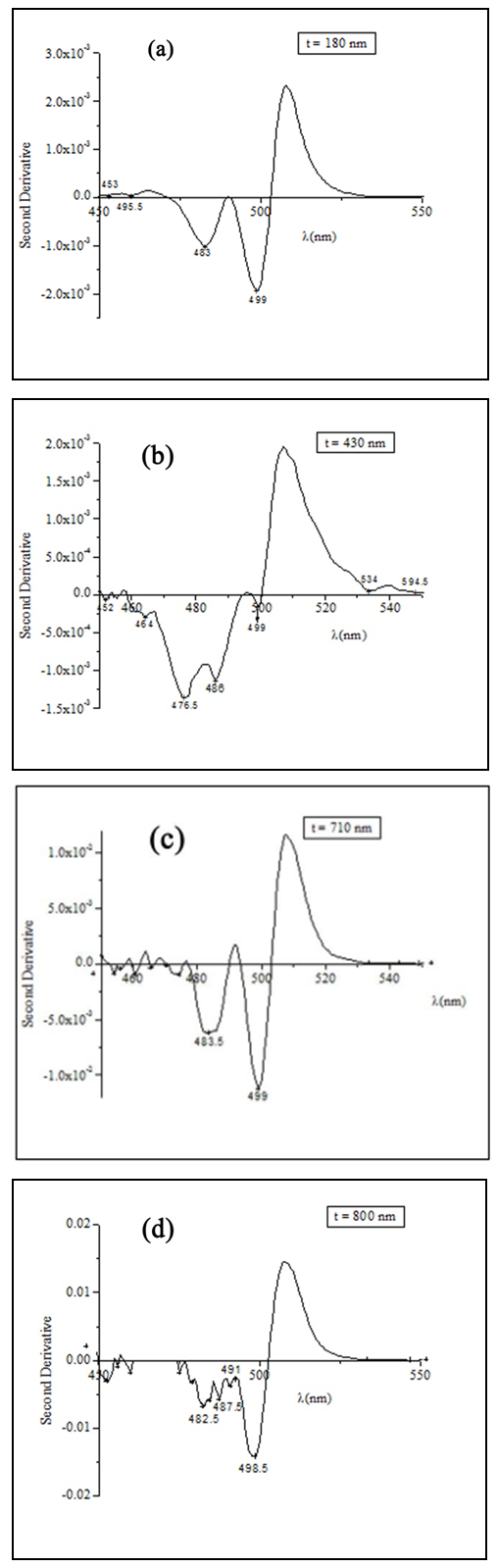
Figure 5. The second derivative of CdS:In thin films of different thickness
Ando et. al [35] gave the known A, B, and C exciton energies as 2.554 eV, 2.569 eV, and 2.632 eV in bulk CdS crystals at 4.2 K, respectively. These values are larger than the values obtained in this work. A main reason is that those of the bulk are given at 4.2 K while these values are obtained at room temperature, where location and intensity of exciton peaks depend on temperature [36]. Ando et. al [35] obtained two peaks for CdS nanocrystals in Al2O3 matrices formed by sequential ion implantation at 2.611 and 2.681 eV respectively where they ascribed the first one to the merged A and B exciton peaks and the second to the C free exciton peak. The larger values obtained by Ando et. al [35] are due to quantum size effect of nanocrystals.
The values that obtained in Fig.3b are close to the values obtained by Dułak and Męczyńska [37] for CdS thin films of thickness 700-900 nm prepared by the SP technique where they studied the optical properties of the excitonic region as a function of ph. They [37] found the best values of the three characteristic exciton peaks of CdS at ph = 5.7 and peak A is at 487.5 nm, peak B at 484.4 nm, and peak C at 472.5 nm. Also they found that the position of the C peak was shifted by 1.5 nm with respect to the single CdS crystal.
From these results the average energy separation between the merged A and B free exciton peaks and the C free exciton peak is 67.5 ± 15.8 meV. The large error is due to the overlap of the different peaks beside the quantum size effect which made a shift of the positions as mentioned before. This value is in good agreement with the known value for the difference between B and C free exciton energies in the bulk CdS which is 63 meV. On the other hand, it is closer to the separation between the mean energy of the A and B excitons and the C exciton energy in bulk CdS crystals which is 70.5 meV.

4. Conclusions

Indium doped cadmium sulphide thin films were produced on glass substrates by the spray pyrolysis technique. XRD diffractogram showed that the films have predominantly wurtzite structure. SEM micrographs showed that that the films are polycrystalline with grains of deformed hexagonal and cubic shapes. EDS report showed that the films are cadmium rich and contain indium. The second derivative of the absorbance was used to detect the peaks in the absorption spectrum. The merged A and B free exciton peak and C free exciton peak of the hexagonal phase were observed and their energies were deduced and compared with those obtained by different authors. The separation between the merged A and B free exciton peaks and that of the C free exciton peak was calculated and found to be in good agreement with that of the bulk and with that obtained by different authors. The bandgap energy of the zinc-blined was obtained and found to be in good agreement with that in the literature.

References

[1]  A.P. Samantilleke, M.F. Cerqueira, S. Heavens, P. Warren, I.M. Dharmadasa, G.E.A. Muftah, C.J.R. Silva, B. Marí, Characterisation of chemical bath deposited CdS thin films on different substrates using electrolyte contacts, Thin Solid Films (2011), doi:10.1016/j.tsf.2010.12.218.
[2]  H. Ariza-Calderon, R. Lozada- Morales, O. Zelaya-Angel, J. G Mendoza- Alvarez and L. Baños, Photoluminescence measurements in the phase transition region for CdS thin films, J. Vac. Sci. Technol. A. 14(4) (1996) 2480-2482.
[3]  A. Graf, N. Maticiuc, N. Spalatu, V. Mikli, A. Mere, A. Gavrilov, J. Hiie, Electrical characterization of annealed chemical-bath-deposited CdS films and their application in superstrate configuration CdTe/CdS solar cells, Thin Solid Films 582 (2015) 351–355.
[4]  Biswajit Ghosh, Kamlesh Kumar, Balwant Kr Singh, Pushan Banerjee, Subrata Das, Growth of CdS thin films on indium coated glass substrates viachemical bath deposition and subsequent air annealing, Applied Surface Science 320 (2014) 309–314.
[5]  Amanullah Fatehmulla, A.S. Al-Shammari, A.M. Al-Dhafiri, W.A. Farooq and F. Yakuphanoglu, Structural, electrical and optical properties of chlorine doped CdS thin films, World Applied Sciences Journal 31 (12) (2014): 2073-2078.
[6]  G. Perna, V. Capozzi, M. Ambrico, V. Augelli, T. Ligonzo, A. Minafra, L. Schiavulli and M. Pallara. Structural and optical characterization of undoped CdS films grown by pulsed laser deposition. Thin Solid Films 453-454 (2004) 187-194.
[7]  N.M. Megahid, M.M. Wakkad, E.KH. Shokr, N.M. Abass, Microstructure and electrical conductivity of In-doped CdS thin films, Physica B 353 (2004) 150–163.
[8]  T.D. Dzhafarov, F. Ongul, S. Aydin Yuksel, Effect of indium diffusion on characteristics of CdS films and nCdS/pSi Heterojunctions, Vacuum 84 (2010) 310–314.
[9]  G. Perna, V. Capozzi, M. Ambrico, V. Augelli, T. Ligonzo, A. Minafra, L. Schiavulli, M. Pallara, Structural and optical characterization of undoped and indium-doped CdS films grown by pulsed laser deposition, Thin Solid Films 453 –454 (2004) 187–194.
[10]  C.T. Tsai, D.S. Chuu, G.L. Chen, S.L. Yang,. Studies of grain size effects in rf sputtered CdS thin films. J. Appl. Phys. 79 (1996) 9105–9109.
[11]  J. Aguilar-Hernández, J. Sastré-Hernández, R. Mendoza-Pérez, G. Contreras-Puente, M. Cárdenas-García, J. Ortiz-López. Photoluminescence studies of CdS thin films annealed in CdCl2 atmosphere. Solar Energy Materials & Solar Cells 90 (2006): 704–712.
[12]  Anke E. Abken, D. P. Halliday, and Ken Durose. Photoluminescence study of polycrystalline photovoltaic CdS thin film layers grown by close-spaced sublimation and chemical bath deposition. J. Appl. Phys. 105 (2009): 064515.
[13]  G. Perna, V. Capozzi, M. Ambrico, V. Augelli, T. Ligonzo, A. Minafra, L. Schiavulli, M. Pallara, Structural and optical characterization of undoped and indium doped CdS films grown by pulsed laser deposition, Thin Solid Films 453-454 (2004): 187-194.
[14]  G. Perna, V. Capozzi, S. Pagliara, M. Ambrico. Absorption and photoluminescence analysis of CdS ablated films grown on quartz substrate. Applied Surface Science 154–155(2000): 238–243.
[15]  Shadia. J. Ikhmayies, "Production and characterization of CdS/CdTe thin film photovoltaic solar cells of potential industrial use". (Ph.D Thesis. University of Jordan, 2002).
[16]  Shadia J. Ikhmayies and Riyad N Ahmad-Bitar, Effects of annealing in nitrogen atmosphere and HCl-etching on the photoluminescence spectra of spray-deposited CdS:In thin films, Applied Surface Science 255 (20) (2009): 8470-8474.
[17]  Shadia J. Ikhmayies and Riyad N Ahmad-Bitar, Direct observation of infrared photoluminescence of spray-deposited CdS:In thin films, J. Luminouscence, 128(4), (2008): 615-619.
[18]  Shadia J. Ikhmayies and Riyad N. Ahmad-Bitar, Effect of film thickness on the electrical and structural properties of CdS: In thin films, American Journal of Applied Sciences 5 (9) (2008) 1141-1143.
[19]  Shadia J. Ikhmayies and Riyad N. Ahmad-Bitar, Effects of processing on the electrical and structural properties of spray-deposited CdS:In Thin Films, Physica B: Condensed Matter 404 (16) (2009) 2419-2424.
[20]  Shadia J. Ikhmayies and Riyad N. Ahmad-Bitar, The Influence of the substrate temperature on the photovoltaic properties of spray-deposited CdS:In thin films, Applied Surface Science 256 (11) (2010) 3541-3545.
[21]  Shadia J. Ikhmayies and Riyad N. Ahmad-Bitar, A Comparison between the electrical and optical properties of CdS:In thin films for two doping ratios, Jordan Journal of Mechanical and Industrial Engineering JJMIE 4(1) (2010) 111-116.
[22]  Shadia J. Ikhmayies and Riyad N. Ahmad-Bitar, The use of I-V characteristics for the investigation of selected contacts for spray-deposited CdS:In thin films, Vacuum 86 (2011) 324-329.
[23]  Shadia J. Ikhmayies and Riyad N. Ahmad-Bitar, AC Measurements of Spray-Deposited CdS:In Thin Films, J.Cen. South Univ 19 (2012) 829-834.
[24]  Shadia J. Ikhmayies and Riyad N Ahmad-Bitar, A Study of the Optical Bandgap Energy and Urbach Tail of Spray-Deposited CdS:In Thin Films, Journal of Materials Research and Technology, 2(3) (2013) 221-227.
[25]  Shadia J. Ikhmayies, Hassan K. Juwhari and Riyad N Ahmad-Bitar, Nanocrystalline CdS:In Thin Films Prepared by the Spray-Pyrolysis Technique, J. Luminouscence, 141 (2013) 27-32.
[26]  Shadia J. Ikhmayies and Riyad N Ahmad-Bitar, Temperature dependence of the photoluminescence spectra of CdS: In thin, films prepared by the spray pyrolysis technique, Journal of Luminescence 142 (2013) 40-47.
[27]  Shadia J. Ikhmayies and Riyad N Ahmad-Bitar, Dependence of the photoluminescence of CdS:In thin films on the excitation power of the laser, Journal of Luminescence 149, (2014), 240-244.
[28]  Shadia J. Ikhmayies, The Influence of Heat Treatment on the Optical Parameters of Spray-Deposited CdS:In Thin Films, JOM 69 (2) (2017), 144-161.
[29]  Shadia J. Ikhmayies, The influence of heat treatment on the optical parameters of spray-deposited CdS:In thin films, Characterization of Minerals, Metals, and Materials 2016, 427-434..
[30]  Shadia J. Ikhmayies, Optical parameters of spray-deposited CdS:In thin films, TMS2015 Annual Meeting Supplemental Proceedings, 585 – 592.
[31]  Fangyang Liu, Yanqing Lai, Jun Liu, Bo Wang, Sanshuang Kuang, Zhian Zhang, Jie Li, Yexiang Liu, Characterization of chemical bath deposited CdS thin films at different deposition temperature, Journal of Alloys and Compounds 493 (2010) 305-308.
[32]  M. Ando, Y. Kanemitsu, T. Kushida, K. Matsuda, T. Saiki, and C. W. White, Sharp photoluminescence of CdS nanocrystals in Al2O3 matrices formed by sequential ion implantation, Applied Physics Letters. 79 (4) (2001), 539-541.
[33]  T. S. Jeong, P. Y. Yu, and T. S. Kim, Temperature dependence of the free excitons in a CdS single crystal, Journal of the Korean Society 36 (2) (2000), 102-105.
[34]  W. Dułak and H. Męczyńska, Exciton spectra of thin CdS films prepared by spray pyrolysis, Phys. Stat. Sol. (A) 93 (1986), K1 71.