-
Paper Information
- Paper Submission
-
Journal Information
- About This Journal
- Editorial Board
- Current Issue
- Archive
- Author Guidelines
- Contact Us
International Journal of Materials and Chemistry
p-ISSN: 2166-5346 e-ISSN: 2166-5354
2017; 7(2): 36-46
doi:10.5923/j.ijmc.20170702.03

Temperature Dependent Properties of Spray Deposited Nanostructured ZnO Thin Films
 Abstract
 Reference
 Full-Text PDF
 Full-text HTML
V. P. Deshpande1, S. D. Sartale2, A. N. Vyas2, A. U. Ubale1
1Nanostructured Thin Film Materials Laboratory, Department of Physics, Govt. Vidarbha Institute of Science and Humanities, Amravati, India
2Thin Film and Nanomaterial Laboratory, Department of Physics, University of Pune, India
Correspondence to: A. U. Ubale, Nanostructured Thin Film Materials Laboratory, Department of Physics, Govt. Vidarbha Institute of Science and Humanities, Amravati, India.
| Email: |  |
Copyright © 2017 Scientific & Academic Publishing. All Rights Reserved.
This work is licensed under the Creative Commons Attribution International License (CC BY).
http://creativecommons.org/licenses/by/4.0/

In present investigation, the effect of substrate temperature on structural, optical and electrical properties of spray deposited nanostructured ZnO thin films is studied. XRD studies showed that films are polycrystalline in nature with hexagonal structure. Optical studies revealed the decrease in band gap from 3.31 to 3.23 eV with increase in substrate temperature. The dark electrical resistivity measurement was done by two probe method. It is of the order of 10-2 ohm-cm. From TEP measurement it was confirmed that the ZnO films exhibits n-type conductivity. Seebeck’s coefficient was also calculated from TEP graph. It is of the order of 8-45 µVK-1.
Keywords: Zinc Oxide, Thin films, Chemical spray pyrolysis technique
Cite this paper: V. P. Deshpande, S. D. Sartale, A. N. Vyas, A. U. Ubale, Temperature Dependent Properties of Spray Deposited Nanostructured ZnO Thin Films, International Journal of Materials and Chemistry, Vol. 7 No. 2, 2017, pp. 36-46. doi: 10.5923/j.ijmc.20170702.03.
Article Outline
1. Introduction
- In the last decades, research regarding the physical properties of the transparent conducting oxides (TCO) thin films has intensively motivated the research community due to their wide-ranging applications in flat panel display, light emitting diodes and photovoltaic cells [1]. Zinc oxide is one of the important member amongst TCOs. ZnO is commercially available with advantages such as comparatively low cost, environment-friendly non-toxic nature, high resistance to radiation damage, and high thermal and chemical stability. Chemically, ZnO is a simple compound; morphologically, however, this material is very rich in terms of the geometry of its particles. The n-type character of as-grown ZnO has often been attributed to VO and Zni within the ZnO network. It is the deviation from stoichiometry as a result of the presence of the intrinsic native point defects that makes ZnO semiconducting. There are several research groups working all over the world, aiming at the modification of zinc oxide (ZnO) as an alternative to costly ITO [2-4]. Many researchers focused on the investigation of the relationship between the synthesis route of ZnO and its physical properties [5-10]. ZnO particles were largely prepared by using “wet” chemistry or pyrolysis, whereas the vacuum techniques prevailed in making thin ZnO films. The starting zinc compound, chemical composition of solvent, nature of the precipitating agent, pH, temperature, and time of aging influence the size and geometrical shape of ZnO particles [11].Various methods have been employed for deposition of ZnO based thin films. Such as chemical vapor deposition, thermal evaporation, magnetron sputtering, pulsed laser deposition (PLD), laser chemical vapor deposition, and non-vacuum methods, namely, successive ionic layer absorption and reaction (SILAR), sol-gel spin coating, spray pyrolysis and screen printing [12-20]. The quality and properties of the spray deposited film highly depends on the various process parameters such as spray rate, substrate temperature, nozzle to substrate distance, quantity of spray solution, and precursor concentration. However, the most important parameter is the substrate temperature as it highly affects the film morphology. The higher the substrate temperature, the rougher and more porous are the films. If the temperatures are too low the films are cracked. In between, dense and smooth films can be obtained. The deposition temperature also influences the crystallinity, texture and other physical properties of the deposited films. The present study is focused on the influence of substrate temperature on structural, optical and electrical properties of zinc oxide films deposited by spray pyrolysis technique.
2. Experimental Details
- Zinc oxide thin films were deposited by means of chemical spray pyrolysis technique by varying substrate temperatures from 150°C to 400°C in the step of 50°C. (Here after the samples deposited at 150°C, 200°C, 250°C, 300°C, 350°C and 400°C are referred as C1, C2, C3, C4, C5 and C6 respectively). Prior to the deposition, the glass substrates were cleaned as discussed in earlier report [21]. For deposition of ZnO films, 0.1M zinc acetate ((CH3COO)2 Zn.2H2O) (AR grade) was prepared with distilled water. Ammonia was used to maintain the pH of solution at 10. The atomization of the solution into a spray of fine droplets was carried out by spray nozzle, with the help of compressed air as carrier gas. During the course of spray, the substrate temperature was monitored using a chromel alumel thermocouple. All the preparative parameters are optimized and discussed earlier [22].
3. Results and Discussion
3.1. XRD Analysis
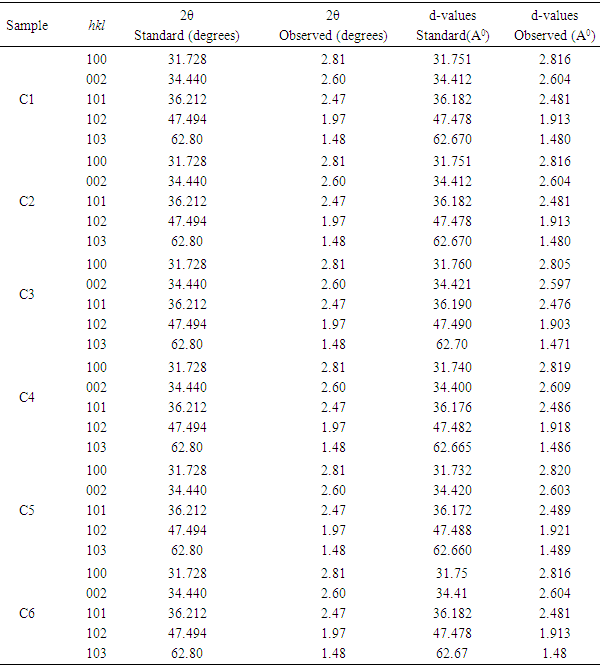
- Figure (1) shows the XRD patterns of ZnO thin films deposited at different temperatures. It reveals that ZnO thin films are nanocrystalline in nature having hexagonal wurtzite structure, which is confirmed from JCPDS card no. 80-0075 [23]. Comparison of standard JCPDS data and observed values is shown in table 1. As reported by several authors [24, 25], our spray deposited ZnO films has preferred orientation along (002). The increase in peak intensity with substrate temperature confirms that crystallinity of ZnO increases with deposition temperature. However, the decrease in the intensity of the peak for sample C6 (ZnO deposited at 400°C) might be due to relatively lower thickness of the film caused by evaporation of primary ingredients before reaching the surface of the substrate.
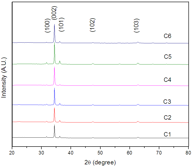 | Figure 1. XRD pattern of ZnO thin films deposited at deposited at (C1) 150°C, (C2) 200°C, (C3) 250°C, (C4) 300°C, (C5) 350°C and (C6) 400°C temperatures |
|
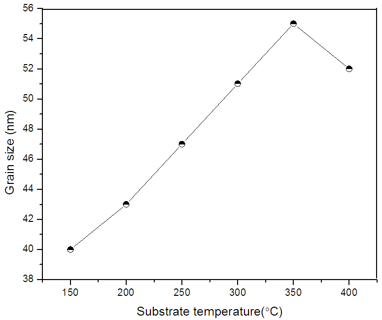 | Figure 2. Variation of grain size of ZnO films with substrate temperature |
 | (1) |
 | (2) |
 is FWHM, and
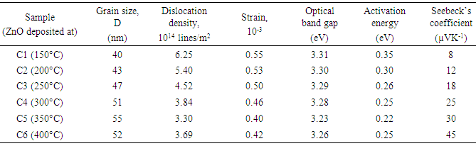
  is glancing angle. Values of lattice strain and dislocation density are listed in table 2. The total stress in the film commonly consists of two components. One is the intrinsic stress introduced by impurities, defects and lattice distortions in the crystal, and the other is the extrinsic stress introduced by the lattice mismatch and thermal expansion coefficient mismatch between the film and substrate. The strain in the films is likely to be of intrinsic, rather than of thermal origin. The thermal strain introduced by the different linear thermal expansion coefficients of a film (αZnO = 410-6 K-1) and glass substrate (αglass=910-6 K-1) is significantly smaller than the measured strain. It shows that the measured film stress is mainly caused by the growth process itself. The lattice strain is maximum for film deposited at 150°C, and it decreases as the deposition temperature increases. The decrease in strain at higher substrate temperatures is attributed to annealing effects and consequent reduction in defects [28].
|
 | (3) |
3.2. SEM Studies
- Figure (3) shows the SEM images of ZnO thin films. All images are homogeneous and have dense surfaces. The increase in grain size with deposition temperature is clearly observed in figure. Initially the grains deposited are spherical in shape. However as the substrate temperature increases, the spherical grains grow further and truned to flakes like structure. However above the optimum substrate temperature 350°C, morphology again turns to the spherical one with smaller grains. It strongly adheres to the substrates and has tightly bounded particles.
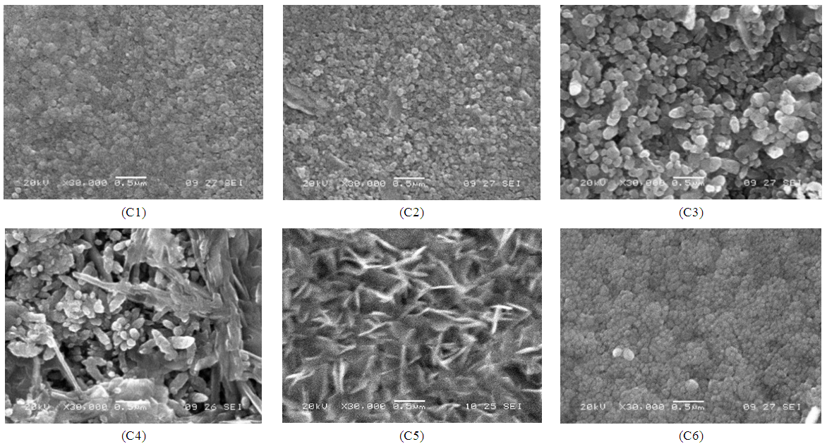 | Figure 3. SEM of ZnO films deposited at (C1) 150°C, (C2) 200°C, (C3) 250°C, (C4) 300°C, (C5) 350°C and (C6) 400°C temperatures |
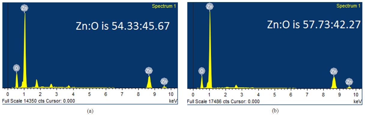 | Figure 4. EDAX spectra of ZnO films deposited at (a) 200°C and (b) 350°C |
3.3. Optical Studies
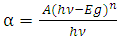
- The optical absorption of ZnO thin films was studied in the wavelength range 350–850 nm and shown in figure (5). The nature of the transition (direct or indirect) was determined by using the relation,
 | (4) |
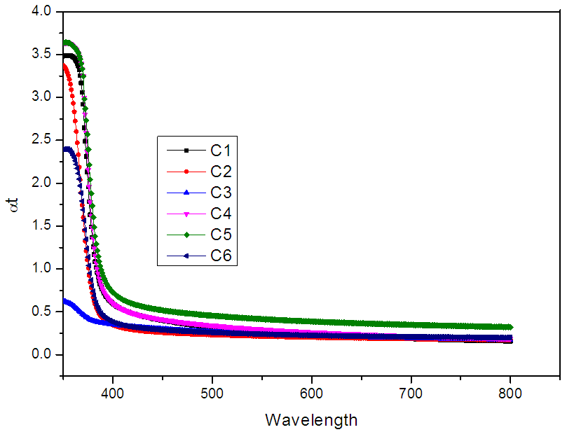 | Figure 5. Variation of absorbance of ZnO films deposited at (C1) 150°C, (C2) 200°C, (C3) 250°C, (C4) 300°C, (C5) 350°C and (C6) 400°C temperatures |
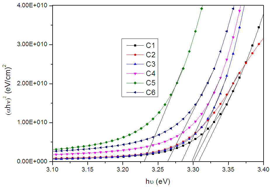 | Figure 6. Plot of (αhν)2 Vs hν of ZnO films deposited at (C1) 150°C, (C2) 200°C, (C3) 250°C, (C4) 300°C, (C5) 350°C and (C6) 400°C temperatures |
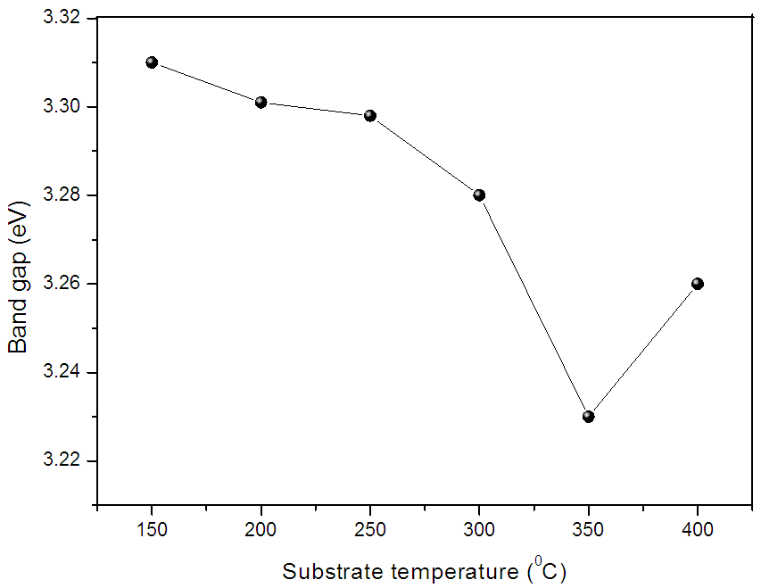 | Figure 7. Variation of band gap of ZnO films with substrate temperature |
3.4. Photoluminescence Studies
- Figure (8) shows the deconvolution of room temperature PL emission spectrum for ZnO sample measured in the wavelength range of 350–650 nm at an excitation wavelength of 330 nm. The ZnO emission is generally classified into two categories. One is the UV emission of the near band edge in the UV region related to free-exciton recombination and the other is the deep-level (DL) emission in the visible range. Especially, the deep-level emission in the ZnO thin films has been attributed to structural defects such as oxygen vacancies and interstitial zinc [36]. In present case, the film shows strong emission at ∼389 nm, attributed to near band edge UV luminescence of ZnO [37]. A broad, low intense peak is found around 600 nm i.e. in green yellow region, which is known to arise from oxygen defects and zinc interstitials [38].
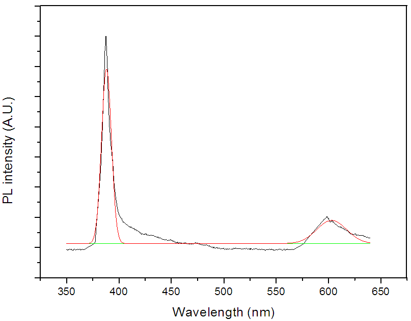 | Figure 8. Deconvolution of PL spectra of ZnO thin film deposited at 350°C |
3.5. Electrical Resistivity
- Figure (9) shows the variation of the dark electrical resistivity with temperature. It was observed that the resistivity of ZnO thin film decreases with increase in temperature, indicating its semiconducting electrical behaviour. The electrical resistivity is of the order of 10-2 to 101 ohm-cm. The films deposited at lower temperature shows higher resistivity than deposited at 350°C. The electrical conduction in ZnO is dominated by electrons generated from O2− vacancies and Zn interstitials. The higher the crystal orientation the lower the resistivity. In fact, this is due to the reduction in the scattering of the carriers at the grain boundaries and crystal defects, which increases the carrier mobility [39, 40].
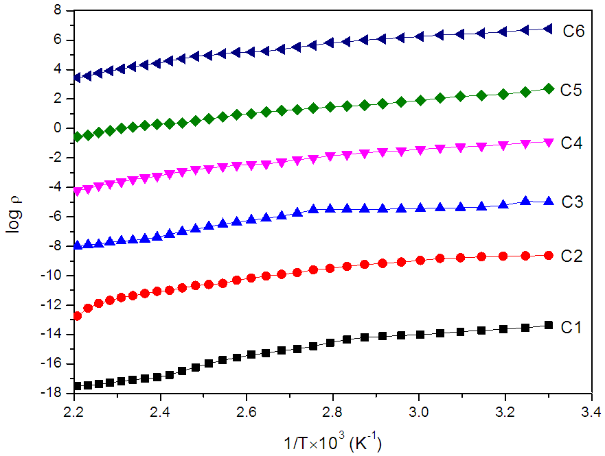 | Figure 9. Variation of log Vs 1/T×103 (K−1) for ZnO thin films deposited at (C1) 150°C, (C2) 200°C, (C3) 250°C, (C4) 300°C, (C5) 350°C and (C6) 400°C temperatures |
 | (5) |
 is resistivity at temperature T,
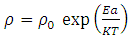
  is a constant, K is Boltzmann’s constant and is Ea the activation energy required for conduction. Variation of activation energy of ZnO thin film with substrate temperature is shown in figure (10). It is found that activation energy is low for the films deposited at 350°C substrate temperature. The decrease in Ea with increase in substrate temperature may be attributed to change in intercrystalline barrier height caused by the grain size variation.
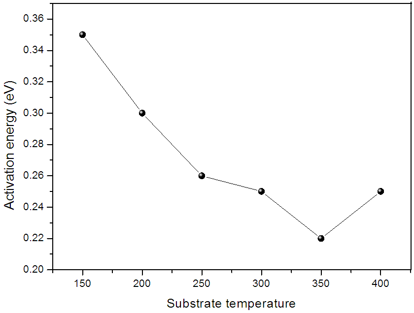 | Figure 10. Variation of activation energy of ZnO films with substrate temperature |
3.6. Thermo Electric Power Measurement
- The temperature gradient applied across the sample causes the transport of carriers from hot to cold end and thus create field which gives thermal voltage. The variation of thermo emf with temperature difference for ZnO films is shown in Figure (11). From thermo emf measurement it was observed that the polarity of thermally generated voltage at the hot end is positive indicating that films are of n-type. The Seebeck’s coefficient was determined by calculating the slope of the thermoelectric emf versus the temperature difference between the hot and the cold end of the samples. The value of
 i.e. Seeback coefficient is listed in table 2. It is observed that, the Seebeck’s coefficient
  increases as deposition temperature increases. The relatively high thermoelectric emf of thin films is due to its higher crystallinity and crystallite size.
 | Figure 11. Variation of thermo emf with temperature difference applied across ZnO films deposited at (C1) 150°C, (C2) 200°C, (C3) 250°C, (C4) 300°C, (C5) 350°C and (C6) 400°C temperatures |
4. Conclusions
- 1. In present chapter the effect of substrate temperature on structural, optical and electrical properties of ZnO thin films is studied. For that ZnO thin films were successfully deposited by chemical spray pyrolysis technique in temperature range 150 to 400°C. 2. XRD results showed that ZnO films have pollycrystalline nature with hexagonal wurtzite structure. The grain size of ZnO increases with substrate temperature. Scanning electron micrograph shows dense structure with spherical grains. At higher temperature this grains grows and exhibits flakes like structure. 3. The observed band gap of ZnO thin films decreases from 3.31 to 3.23 eV with substrate temperature. Photoluminescence study revealed that strong emission at ∼389 nm, attributed to near band edge UV luminescence of ZnO. 4. A dark electrical resistivity of ZnO films is calculated by two probe method. It is in the ranged of 10-2 to 101 ohm-cm. The activation energy decreases from 0.35 to 0.22 eV nm for substrate temperature 150 to 350°C and then again increases to 0.25 eV for 400°C. From thermo electric measurement it is observed that the spray deposited ZnO films have n-type conductivity. The Seebeck’s coefficient was calculated from the slope of thermo emf graph. Value coefficient α increases from 8 to 45 µV/K with substrate temperature. 5. It is therefore concluded that, the properties of ZnO thin films can be tailored simply by controlling the substrate temperature, which in turn may be employed for a specific application. All the results are summarized in table 2.
ACKNOWLEDGEMENTS
- Author is thankful to Deparment of Physics, University of Pune, Pune. The work is partially supported by Departmental Research Development Program of University of Pune, Pune.