| [1] | J. A. Glasscock, P. R. F. Barnes, I. C. Plumb, A. Bendavid, P. J. Martin, “Structural, optical and electrical properties of undoped polycrystalline hematite thin films produced using filtered arc deposition”, Thin Solid Films, vol.516, pp.1716, 2008. |
| [2] | J. Mallinson, The Foundations of Magnetic Record- ing, second ed., Academic Press, New York, 1993. |
| [3] | S. Wang, W. Wang, W. Wang, Z. Jiao, J. Liu, Y. Qian, “Characterization and gas-sensing properties of nano-crystalline iron_III/oxide films prepared by ultrasonic spray pyrolysis on silicon”, Sens. Actuators B vol.69, pp. 22, 2000. |
| [4] | S. Wang, L. Wang et al., “Porous α-Fe2O3 hollow microspheres and their application for acetone sensor”, J. Solid State Chem., vol. 183, pp. 2869, 2010. |
| [5] | D. Patil, V. Patil, P. Patil, “Highly sensitive and selective LPG sensor based on α-Fe2O3 nanorods”, Sens. Actu. B, vol. 152, pp. 299, 2011. |
| [6] | M. Aronniemi, J. Saino, J. Lahtinen, “Characterization and gas-sensing behavior of an iron oxide thin film prepared by atomic layer deposition” Thin Solid Films, vol. 516, pp. 6110, 2008. |
| [7] | M. Pelino, C. Colella, C. Cantalini, M. Faccio, G. Ferri, A. D’Amico, “Microstructure and electrical properties of an C–hematite ceramic humidity sensor”, Sens. Actuators B, vol.7, pp. 464, 1992. |
| [8] | H. Kitaura, K. Takahashi, F. Mizuno, A. Hayashi, K. Tadanaga, M. Tatsumisago, “Mechanochemical synthesis of α-Fe2O3 nanoparticles and their application to all-solid-state lithium batteries”, J. Power Sources, vol. 183, pp.418, 2008. |
| [9] | P. M. Kulal, D. P. Dubal, C. D. Lokhande, V. J. Fulari, “Chemical synthesis of Fe2O3 thin films for supercapacitor application”, J. Alloys Comp., vol. 509, pp. 2567, 2011. |
| [10] | M. Frites, Y. A. Shaban, S. U.M. Khan, “Iron oxide (n-Fe2O3) nanowire films and carbon modified (CM)-n-Fe2O3 thin films for hydrogen production by photosplitting of water” Int. J. hydrogen energy, vol. 35, vol. 4944, 2010. |
| [11] | J. H. Kennedy, D. J. Dunnwald, “Photooxidation of organic compounds at α-Fe2O3 electrodes”, Electro-chem. Soc., vol. 130, pp. 2013, 1983. |
| [12] | J. S. Im, S. K. Lee, Y. S. Lee, “Cocktail effect of Fe2O3 and TiO2 semiconductors for a high performance dye-sensitized solar cell”, Appl. Surf. Sci., vol. 257, pp. 2164, 2011. |
| [13] | J. C. Galan, R. Almanza, “Solar filters based on iron oxides used as efficient windows for energy savings”, Solar Energy, vol. 81, pp. 13, 2007. |
| [14] | V. Sreeja, P. A. Joy,” Microwave–hydrothermal synthesis of γ-Fe2O3 nanoparticles and their magnetic proper- ties”, Mater. Res. Bull., vol. 42, pp. 1570, 2007. |
| [15] | J. Du, H. Liu, “Preparation of super paramagnetic γ-Fe2O3 nanoparticles in nonaqueous medium by γ -irradiation” J. Magn. Magn. Mater., vol. 302, pp. 263, 2006. |
| [16] | X. Jing, Y. Haibin, F. Wuyou, D. Kai, Y. Sui, J. Chen, Y. Zeng, M. Li, G. Zou, J. Magn. Magn. Mater., vol. 309, pp. 307, 2007. |
| [17] | B. Fang, G. Wang, W. Zhang, M. Li, X. Kan, “Fabrication of Fe3O4 nanoparticles modified electrode and its application for voltammetric sensing of dopamine”, Electroanalysis, vol. 17, pp.744, 2005. |
| [18] | A. K. Gupta, M. Gupta, “Synthesis and surface engineering of iron oxide nanoparticles for biomedical applications”, Biomater., vol. 26, pp. 3995, 2005. |
| [19] | R. N. Goyal, D. Kaur, A. K. Pandey, “Growth and characterization of iron oxide nanocrystalline thin films via low-cost ultrasonic spray pyrolysis”, Mater. Chem. Phys., vol.116, pp. 638, 2009. |
| [20] | A. A. Akl, “Microstructure and electrical properties of iron oxide thin films deposited by spray pyrolysis” Appl. Surf. Sci., vol. 221, pp. 319, 2004. |
| [21] | J. Hua, Y. Heqing, “Thermal decomposition synthesis of 3D urchin-like α-Fe2O3 superstructures”, Mater. Sci. Engg. B., vol. 156, pp. 68, 2009. |
| [22] | Y. J. Park, K. M. A. Sobahan, C. K. Hwangbo, “Optical and structural properties of Fe2O3 thin films prepared by ion-beam assisted deposition”, Surf. Coat. Technol., vol. 203, pp. 2646, 2009. |
| [23] | S. S. Kulkarni, C. D. Lokhande, “Structural, optical, electrical and dielectrical properties of electrosynth-sized nanocrystalline iron oxide thin films”, Mater. Chem. Phys., vol.82, pp. 151, 2003. |
| [24] | J. D. Uribe, J. Osorio, C. A. Barrero, D. Girata, A. L. Morales, A. Hoffmann, “Physical properties in thin films of iron oxides”, J. Microelectro., vol. 39, pp.1391, 2008. |
| [25] | H. G. Cha, C. W. Kim, Y. H. Kim, M. H. Jung, E. S. Ji, B. K. Das, J. C. Kim, Y. S. Kang, “Preparation and characterization of α-Fe2O3 nanorod-thin film by metal–organic chemical vapor deposition”, Thin Solid Films, vol. 517, pp. 1853, 2009. |
| [26] | K. Shalini, G. N. Subbanna, S. Chandrasekaran, S. A. Shivashankar, “Thin films of iron oxide by low presure MOCVD using a novel precursor: tris (t-butyl-3-oxo- butanoato) iron (III)”, Thin Solid Films, vol.424, pp. 56, 2003. |
| [27] | S. Park, “Preparation of iron oxides using ammonium iron citrate precursor: Thin films and nanoparticles”, J. Solid State Chem., vol. 182, pp. 2456, 2009. |
| [28] | A. U. Ubale, M. R. Belkhedkar, Y. S. Sakhare, A. Singh, C. Gurada, D.C. Kothari, “Characterization of nanostructured Mn3O4 thin films grown by SILAR method at room temperature", Mater. Chem. Phys., vol. 136, pp. 1067, 2012. |
| [29] | M. R. Belkhedkar, A.U. Ubale, Physical properties of nanostructured Mn3O4 thin films synthesized by SILAR method at room temperature for antibacterial application, J. Mol. Struct., vol. 1068, pp. 94, 2014. |
| [30] | A. U. Ubale, A. N. Bargal, “Characterization of nano structured photosensitive (NiS) x (CdS) (1-x) composite thin films grown by successive ionic layer adsorption and reaction (SILAR) route”, Mater. Res. Bull., vol. 46, pp. 1000, 2011. |
| [31] | A. U. Ubale, D. K. Kulkarni, “Studies of size dependent properties of cadmium telluride thin films deposited by Successive Ionic Layer Adsorption and Reaction (SILAR) method”, Ind. Pure. Appl. Phy., vol. 44, pp. 254, 2006. |
| [32] | H. M. Pathan, C. D. Lokhande, “Deposition of metal chalcogenide thin films by successive ionic layer adsorption and reaction (SILAR) method” Bull. Mater. Sci., vol. 27, pp.85, 2004. |
| [33] | W. Y. Hsien, Z. L. Dong, C. F. Li, S. K. Yen, “Characterization of electrolytic deposited α-Fe2O3 thin films on stainless steel as anodes for Li-ion batteries”, Surf. Coat. Tech., vol. 216, pp. 52, 2013. |
| [34] | S. Zhan, D. Chen, X. Jiao, S. Liu, “Facile fabrication of long α-Fe2O3, α-Fe and γ-Fe2O3 hollow fibers using solgel combined co-electrospinning technology”, J. Coll. Interf. Sci., vol. 308, pp. 265, 2007. |
| [35] | J. Sharma, S. K. Tripathi, ‘Effect of deposition pressure on structural, optical and electrical properties of zinc selenide thin films”, Physica B, vol. 406, pp. 1757, 2011. |
| [36] | A. U. Ubale, Y. S. Sakhare, M. V. Bhute, M. R. Belkhedkar, A. Singh, “Size dependent structural, electrical and optical properties of nanostructured iron selenide thin films deposited by Chemical Bath Deposition Method”, Solid State Sci., vol.16, pp. 134, 2013. |
| [37] | A. Boudjemaa, S. Boumaza, M. Trari, R. Bouarab, A. Bouguelia,” Physical and photoelectrochemical characterizations of α-Fe2O3. Application for hydrogen production”, Int. J. hydrogen energy, vol. 34, pp. 4268, 2009. |
| [38] | V. Balouria, A. Kumar, S. Samanta, A. Singh, A. K. Debnath, A. Mahajan, R. K. Bedi, D. K. Aswal, S. K. Gupta,” Nano-crystalline Fe2O3 thin films for ppm level detection of H2S”, Sens. Actu. B, vol. 181, pp. 471, 2013. |
 Abstract
 Reference
 Full-Text PDF
 Full-text HTML


 versus
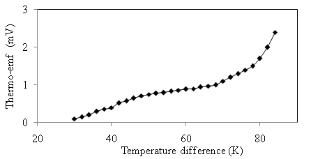
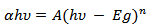
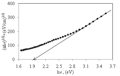
  of α-Fe2O3 film is shown in Figure 10.
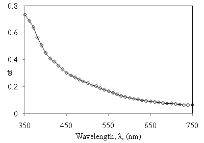
 versus of α-Fe2O3 thin film deposited on to glass substrate
 versus
  for α-Fe2O3 film which confirms the presence of direct transition. The optical direct band gap energy of α-Fe2O3 is found to be 2.97 eV. Both the values of band gap energies are quite more than literature which may be due to quantum confinement in the nanocrystalline α-Fe2O3 [1].
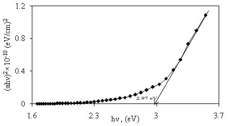
 versus
  of α-Fe2O3 thin film deposited on to glass substrate
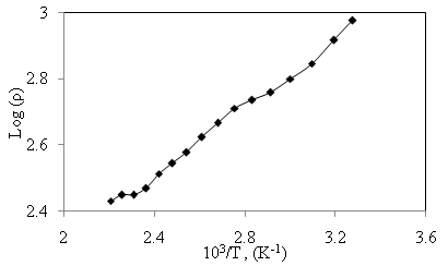
 with reciprocal of temperature. It is clearly seen that the resistivity decreases with increase in temperature indicating semiconducting behavior of α-Fe2O3 . The room temperature electrical resistivity of α-Fe2O3 thin film deposited onto glass substrate by SILAR method is of the order of 9.46 × 10² Ω cm, which is very close to reported value (3 × 10² Ω cm) by A. A. Akl [20] and much less as compared to earlier reports (104 Ω cm) [24]. The activation energy was calculated using relation,
 is constant, K is Boltzmann constant and
  is activation energy. The activation energy of α-Fe2O3 thin film deposited onto glass substrate was found 0.1 eV which is in good agreement with the earlier reports [37].