-
Paper Information
- Paper Submission
-
Journal Information
- About This Journal
- Editorial Board
- Current Issue
- Archive
- Author Guidelines
- Contact Us
International Journal of Materials and Chemistry
p-ISSN: 2166-5346 e-ISSN: 2166-5354
2014; 4(2): 27-33
doi:10.5923/j.ijmc.20140402.02
Micro-Raman Characterization of Effects of Zn Alloying and of in Doping to CdTe
 Abstract
 Reference
 Full-Text PDF
 Full-text HTML
Theodore Ganetsos1, Eduard Belas2, Lukas Cedovy2, Bill Kotsos1, Nikos Laskaris1
1Department Department of Electronics, TEI of Sterea Ellada, Lamia, 35100, Greece
2Faculty of Mathematics and Physics, Charles University, Prague, 12116, Czech Republic
Correspondence to: Theodore Ganetsos, Department Department of Electronics, TEI of Sterea Ellada, Lamia, 35100, Greece.
| Email: |  |
Copyright © 2014 Scientific & Academic Publishing. All Rights Reserved.
Cadmium telluride(CdTe) is unique among II–VI compounds which makes it important and quite suitable for several applications as it may exhibit both n- and p-types conductivity. It is one of the few II–VI compounds that are usually used as absorbers for photovoltaic devices. In this research work we studied In-doped CdTe and CdZnTe after annealing using for investigation the technique of micro-Raman spectroscopy.
Keywords: CdTe, Micro-Raman, CdZnTe, Optical Properties
Cite this paper: Theodore Ganetsos, Eduard Belas, Lukas Cedovy, Bill Kotsos, Nikos Laskaris, Micro-Raman Characterization of Effects of Zn Alloying and of in Doping to CdTe, International Journal of Materials and Chemistry, Vol. 4 No. 2, 2014, pp. 27-33. doi: 10.5923/j.ijmc.20140402.02.
Article Outline
1. Introduction
- In general, infrared optical materials are insulators or semiconductors as judged by their band-gaps and resistivity. Photons of light corresponding to energy greater than the band-gap of the solid are strongly absorbed at the surface. [1-2] As the wavelength is increased and the photon energy is decreased below the band-gap, light is transmitted through the solid. The beginning of light transmission of a solid occurs at the wavelength that corresponds to the band-gap energy. The absorption of the photon is a very strong, quantized electronic transition. One may think of this energy as representing the average ionization energy for the primary chemical bonds formed between the atoms that make up the solid. If the required ionization energy is large enough, transmission begins in the ultraviolet region of the spectrum, as in the case for alkali halides or alkaline earth halides. Then the solid appears water-clear or colorless. If it occurs in the visible region, the solid appears colored. If the absorption edge occurs in the infrared region, the solid appears metallic because all visible light is strongly absorbed and reflected.
2. Experimental
- Considerable change in optical, electrical, and mechanical properties of CdTe thin films is produced by doping and annealing conditions [3]. Moreover p-type and n-type doping of CdTe is easy to achieve. All samples we studied are CdTe doped with Indium and CdZnTe. All samples were grown by the Vertical gradient freeze method directly from the melt [3], where In doping was added to the samples. The doping concentration was 5x1015 cm-3. Electrical conductivity – mobility was measured using the Van der Paw method. The data tabulated in Table 1 shows the electrical properties of the samples and the annealing conditions of each sample.
 | Figure 1. A micro-Raman spectrum of CdZnTe 15%Zn, undoped, as-grown |
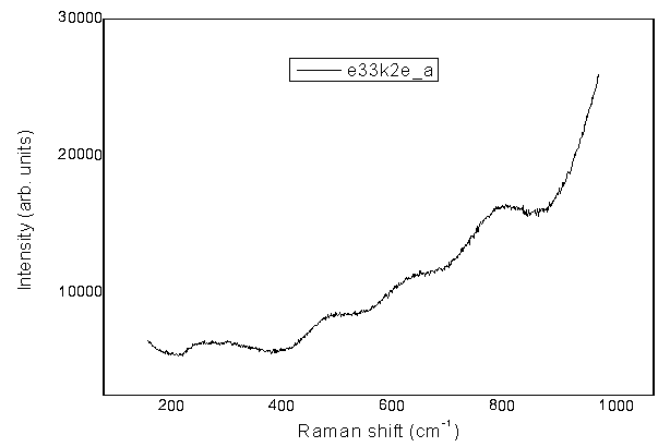
 | Figure 2. A micro-Raman spectrum of CdZnTe 15%Zn, undoped, after Cd-rich annealing (24 hours) |
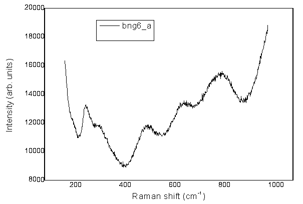 | Figure 3. A micro-Raman spectrum of CdZnTe 15%Zn, undoped, after Cd-rich annealing (48 hours) |
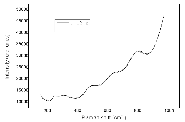
 | Figure 4. A micro-Raman spectrum of CdTe doped with In, after Te-rich annealing |
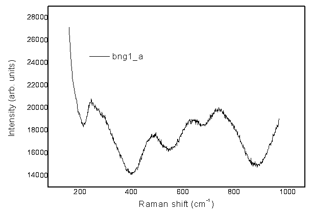
 | Figure 5. A micro-Raman spectrum of CdTe doped with In, as-grown |
3. Results and Discussion
- First, we studied in details the samples of CdZnTe 15% Zn, in the range of 150-550cm-1. Their typical Raman peaks were confirmed, according to the literature [9,10]. A possible origin for a Raman peak identified could be a secondary phonon with A1 symmetry and E symmetry of Te inclusions. A minor difference of the vibrational frequencies related to the annealing temperature towards lower frequencies, as shown in the Figs 6-8 was observed.
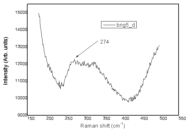 | Figure 6. A micro-Raman spectrum of CdZnTe 15%Zn, undoped, as-grown, in the range 150-550  |
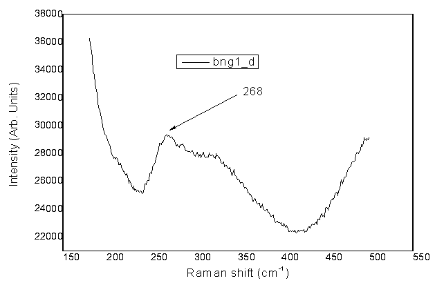 | Figure 7. A micro-Raman spectrum of CdZnTe 15%Zn, undoped, after Cd-rich annealing (24 hours), in the range 150-550  |
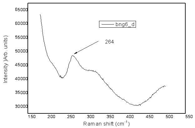 | Figure 8. A micro-Raman spectrum of CdZnTe 15%Zn, undoped, after Cd-rich annealing (48 hours), in the range 150-550  |
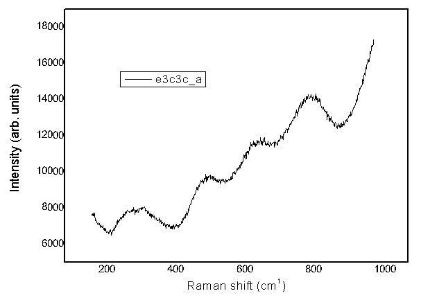
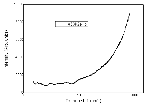 | Figure 9. A micro-Raman spectrum of CdTe doped with In, after Te-rich annealing, in the range 180-2000 |
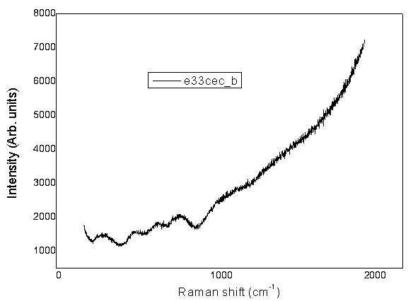 | Figure 10. A micro-Raman spectrum of CdTe doped with In, as-grown, in the range 180-2000  |
4. Concluding Remarks
- It is well known that the resistivity of CdTeIn strongly depends on the In doping concentration and growth and post-annealing conditions. In this research work we studied In-doped CdTe and CdZnTe after annealing at various temperatures using Raman spectroscopy. We present the results of (LO) phonon frequency as function of the temperature. Additional changes are observed in the spectral range above 200 cm-1, where the clean CdTe surface shows the 2LO multiphonon structure at 314 cm-1 in accordance with bibliography [9-10]. The increase in the peak intensity and the decrease in FWHM of the Raman peak for the annealed films indicate the improvement in the crystallinity of the films during thermal annealing.
ACKNOWLEDGEMENTS
- This research work is supported by the Greek General Secretariat of Research and Technology (project code 11CZ_32_ΕΤ33, 7497/19-6-12) Joint Research and Technology Programme Greece-Czech Republic 2011 – 2013. The authors would like to express their special thanks to Dr. M. Perraki for the Micro-Raman measurements.
References
| [1] | R. Hilton, “Chalcogenide for Infrared Optics” Mc Graw Hill, 2010, pp. 52–55. |
| [2] | T. Ganetsos, E. Belas and B. Kotsos, “Electrical properties and Raman study of In-doped effects of CdTe” Procedia Engineering, vol. 25, 2011, pp.354–357. |
| [3] | E. Belas, Grill R., Toth A.L., Moravec P., Horodyský P., Franc J., Höschl P., Wolf H., Wichert Th, “Electrical and optical properties of In-doped CdTe after Cd-rich annealing” IEEE Transactions on Nuclear Science, vol. 52, 2005, pp. 1932–1936. |
| [4] | M. Perraki, Andrey V. Korsakov, David C. Smith, and Evripidis Mposkos, “Raman spectroscopic and microscopic criteria for the distinction of microdiamonds in ultrahigh- pressure metamorphic rocks from diamonds in sample preparation materials”, American Mineralogist, vol. 94, 2009 pp.546-556. |
| [5] | S. H. Wei and S. B. Zhang, “Theoretical Study of Doping Limits of CdTe” National Renewable Energy Laboratory, 2001, pp.1-4. |
| [6] | A. A. Al-Duri et al, “Optical Properties of Al- and Sb-Doped CdTe Thin Films,” Advances in Condensed Matter Physics, vol. 2010, 2010, pp.1-5. |
| [7] | E. Belas, M. Bugár, R. Grill, J. Franc, P. Moravec, P. Hlídek, P. Höschl, “(podíl=70%) Reduction of Inclusions in (CdZn)Te and CdTe:In single crystals by post-growth annealing” , J. Electron. Mater., vol. 37, 2008, pp. 1212-1218. |
| [8] | J. Franc, Grill R., Belas E., Hlídek P., Kubat J., Höschl P., “Characterization of Transport and Charge Collection in high resistivity CdTe photoelectric measurement” ,IEEE Trans. Nucl. Sci., vol. 52, 2005, pp. 1937-1940. |
| [9] | M. G. Sridharan, M. Mekaladevi, Sa.K. Narayandass, D. Mangalaraj, H.Chul Lee, “Raman scattering studies on polycrystalline Cd0.9Zn0.1Te thin films” Journal of Optoelectronics and Advanced Materials Vol. 7, No. 3, June 2005, p. 1479 - 1482. |
| [10] | C. M. Ruiz, O. Vigil, E. Saucedo, G. Contreras-Puente and V. Bermúdez, “Bi doped CdTe: increasing potentialities of CdTe based solar cells”, J. Phys.: Condens. Matter, vol. 18, 2006, pp.7163. |
| [11] | Jiahua Min, Xiaoyan Liang, Jun Chen, Dong Wang, Hui Li, Jijun Zhang, “Investigation of Te inclusions in CdZnTe crystalline material using Raman spectroscopy and IR techniques”, Vacuum, vol. 86, 2012, pp.1003-1006. |