-
Paper Information
- Paper Submission
-
Journal Information
- About This Journal
- Editorial Board
- Current Issue
- Archive
- Author Guidelines
- Contact Us
International Journal of Materials and Chemistry
p-ISSN: 2166-5346 e-ISSN: 2166-5354
2014; 4(1): 1-8
doi:10.5923/j.ijmc.20140401.01
Size Dependent Physical Properties of Spray Deposited Nanocrystalline Cd0.5Fe0.5Se Thin Films
 Abstract
 Reference
 Full-Text PDF
 Full-text HTML
S. G. Ibrahim, A. U. Ubale
Nanostructured Thin Film Materials Laboratory, Department of Physics, Govt. Vidarbha Institute of Science and Humanities, Amravati 444604, Maharashtra, India
Correspondence to: A. U. Ubale, Nanostructured Thin Film Materials Laboratory, Department of Physics, Govt. Vidarbha Institute of Science and Humanities, Amravati 444604, Maharashtra, India.
| Email: |  |
Copyright © 2012 Scientific & Academic Publishing. All Rights Reserved.
Nanostructured Cd0.5Fe0.5Se thin films were successfully deposited onto the glass substrates at 573 K temperature using spray pyrolysis technique. The films of thickness 156 to 290 nm were prepared by changing the quantity of spray solution from 10 to 25 mL. The structural and morphological properties of nanostructured Cd0.5Fe0.5Se thin films were investigated by XRD, EDAX, SEM and AFM analysis respectively. The XRD analysis shows that the spray deposited Cd0.5Fe0.5Se thin films are nanocrystalline in nature with hexagonal crystal structure. The as deposited Cd0.5Fe0.5Se thin films are porous in nature with growth of nanotubes and nanodiscs depending upon quantity of spray solution. The AFM analysis shows uniform growth of Cd0.5Se0.5Fe material that covers the whole substrate. The electrical resistivity of semiconducting Cd0.5Fe0.5Se thin films is of the order of 106 Ωcm and it decreases as the film thickness increases. The thermo-emf measurement confirms the n-type conductivity of Cd0.5Fe0.5Se thin films. The optical band gap energy of the deposited Cd0.5Fe0.5Se thin film increases from 1.74eV to 2.08eV as the film thickness decreases from 290 to 156 nm.
Keywords: Thin films, Nanostructures, Chemical synthesis, Electrical properties,Optical properties
Cite this paper: S. G. Ibrahim, A. U. Ubale, Size Dependent Physical Properties of Spray Deposited Nanocrystalline Cd0.5Fe0.5Se Thin Films, International Journal of Materials and Chemistry, Vol. 4 No. 1, 2014, pp. 1-8. doi: 10.5923/j.ijmc.20140401.01.
Article Outline
1. Introduction
- In the last few years, the science and technology of nanomaterials has created great excitement and expectations in the scientific word. The properties of materials with nanometric dimensions are significantly different from those of atoms or bulk materials which can be significantly utilized to develop new science as well as new products. In this regards the II–VI group semiconducting chalcogenide nanoparticles, especially sulphides and selenides have been investigated extensively owing to their interesting optoelectronic properties[1,2]. Cadmium selenide is important compound semiconductor material because of its major contribution in solar cells, photo detectors, light amplifiers, electrophotography, light emitting diodes, lasers, photoelectrochemical cells, gas sensors and biomedical imaging devices[3–6]. Electrical and optical properties of semiconducting films are very important from application point of view in various optoelectronic devices and these properties are extremely sensitive to ambient conditions and deposition technique used. The study of effect of various deposition parameters such as nature of precursors, type of substrate, deposition temperature, film thickness etc. on physical and chemical properties of the deposited material is necessary in order to explore its application[7,8] Therefore, study of such properties of the films with respect to their different growing as well as ambient conditions is a matter of profound importance. The nanocrystalline film exhibits several interesting phenomena originating from the quantum confinement effect, such as increase in the optical band gap with decrease in crystallite size[9–11]. As per literature few reports were available on chemically deposited Fe based ternary composite thin films such as Pb1−xFexSe[12], Cd1−xFexS[13,14], FeCdS3[15,16], Fe:CdSe [17] Cd-Fe-Se[18] etc. But no report is available on size dependent structural, electrical and optical properties of Cd0.5Fe0.5Se thin films. In the present work, chemical spray pyrolysis method was used to prepare Cd0.5Fe0.5Se thin films of thickness 156 to 290 nm by varying the quantity of spray solution. The effect of film thickness on structural, electrical and optical properties of nanostructured Cd0.5Fe0.5Se thin films is discussed.
2. Experimental Details
- The Cd0.5Fe0.5Se thin films were deposited onto glass substrates using spray pyrolysis technique at 573K temperature. The various deposition parameters were optimized by taking several trails and listed in Table 1. It was observed that in the deposition mechanism the nature of the substrate surface is very important in order to grow uniform film over the entire substrate surface. To get adhesive film, extreme cleaning of the substrate is required, since the contaminated oily substrate surface gives non-uniform and non-adhesive film growth. Hence cleaning of the substrate prior to the actual deposition is important. Commercially available glass micro slides of dimensions 26 mm×76 mm×2 mm were boiled in chromic acid for 30 min, then washed with liquid detergent and rinsed in acetone. Finally slides were ultrasonically cleaned with double distilled water for 15 min prior to the actual deposition. The SeO2 solution was prepared by dissolving 1g of selenium metal powder (99% purity) with 10 mL nitric acid (HNO3). It was then boiled for few minutes to get white residual powder inside the beaker. To it 100 mL of distilled water was added to prepare 0.1 M SeO2 solution. For the deposition of Cd0.5Fe0.5Se thin films the aqueous solutions of 10 mL of 0.1M ferric chloride, 0.1M CdCl2 and 20 mL of 0.1M SeO2 solutions were mixed together to prepare spray solution. It was observed that the films deposited at 573K are well adherent and uniform; however films deposited below were discontinuous and less adhesive, which may be due to incomplete thermal decomposition.
3. Results and Discussion
3.1. Structural Analysis
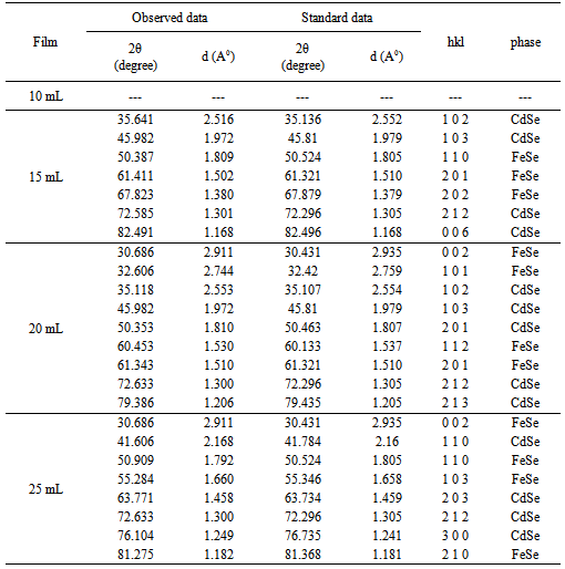
- The structural properties of Cd0.5Fe0.5Se thin films were investigated by X-ray diffraction technique. Figure 1 shows the X-ray diffraction spectra of Cd0.5Fe0.5Se thin films deposited by varying the quantity of spray solution from 10 to 25mL. The observed ‘d’ values were compared with the standard data (JCPDS file CdSe: 80-459,2-230,77-2307 and FeSe: 75-0608) to confirm the structure of the deposited thin films (Table 2). The spray deposited Cd0.5Fe0.5Se thin films are nanocrystalline in nature with mixture of hexagonal CdSe and FeSe phases. The film deposited at 10mL spray solution shows amorphous nature as no prominent peak is observed. It may be because for 10mL of spray solution the film thickness is very small with tiny grains formed on the substrate. These grains are further grown with quantity of spray solution showing peaks in the XRD pattern above 10mL. The observed diffraction peaks at 2Ө angles 35.64, 45.98, 72.58, 82.49, 53.11, 50.35, 72.63, 79.38, 41.60, 63.77, 72.63 and 76.10 degree (marked by *) corresponds to the lattice planes (102), (103), (212), (006), (102), (103), (201), (212), (213), (110), (203), (212) and (300) due to hexagonal CdSe, however the diffraction peaks observed at 2Ө angles 50.38, 61.41, 67.82, 30.68, 32.60, 60.45, 61.34, 30.68, 50.90, 55.28 and 81.27 degree (marked by #) corresponds to lattice planes (110), (201), (202), (002), (101), (112), (201), (002), (110), (103) and (210) due to hexagonal FeSe respectively. The (103) orientation due to hexagonal CdSe is repeated for 15 and 20 mL of spray solution and (212) is repeated for 20 and 25 mL of spray solution while (002) orientation due to hexagonal FeSe is repeated after 20 mL of spray solution. This variation may be due to alloy formation in the film. Pawar et al[20] have reported hexagonal polycrystalline nature for Fe doped CdSe thin films deposited by electrodeposition method. The crystallite size was calculated by using FWHM data and Debye Scherer’s formula.
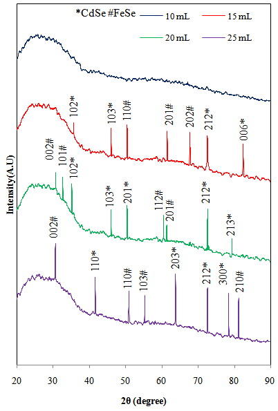 | Figure 1. XRD images of Cd0.5Fe0.5Se thin films deposited by varying the quantity of spray solution |
|
 | (1) |
 | (2) |
 | (3) |
|
3.2. Morphology
- The SEM micrographs of Cd0.5Fe0.5Se thin films deposited by varying quantity of spray solution are shown in Figure 2. It is observed that the deposited Cd0.5Fe0.5Se thin films are homogeneous and porous in nature. At 10 mL of spray solution growth of nano grains on homogeneous background are observed. This grain growth is improved with quantity of spray solution showing well developed nano needle like network at 15mL. However, as the quantity of spray solution is increased above 15 mL growth of nano discs are observed. At 20 mL of spray solution the film surface shows clear overgrowth of well-developed nanodiscs on homogeneous background. The porous network observed at 15 mL spray solution contains number of voids however, above 15 mL spray solution the voids disappear with development of disc structure. The growth of disc structure above 15 mL of spray solution may be due to over deposition of excess quantity of spray solution. To study the stoichiometry of the film quantitative analysis was carried out using the EDAX technique. Figure 3 shows typical EDAX patterns of the Cd0.5Fe0.5Se thin films deposited by varying quantity of spray solution. The elemental analysis was carried out only for Fe, Cd and Se. However, there are some additional peaks corresponding to i, O, Ca, Mg, etc., in the EDAX spectra, which could be due to the presence of these elements in the glass substrate. The average atomic percentage ratio f Cd:Fe:Se are listed in Table 4. It is observed that the elemental composition in the film is almost in good agreement with experimental expected composition of Cd0.5Fe0.5Se.Two-dimensional surface morphology of the spray deposited Cd0.5Fe0.5Se thin films was investigated from atomic force micrographs. Figure 4 shows the 2D AFM images of Cd0.5Fe0.5Se thin films deposited by varying the quantity of spray solution from 10 to 25mL. It can be seen that spray deposited Cd0.5Fe0.5Se thin film have granular structure. In addition to granular nature, the film substrate is dense, uniform with porous nature are observed. Also it is observed that film deposited using 15 mL of spray solution are porous as that of other films, which supports the SEM analysis.
| ||||||||||||||||||||||||||
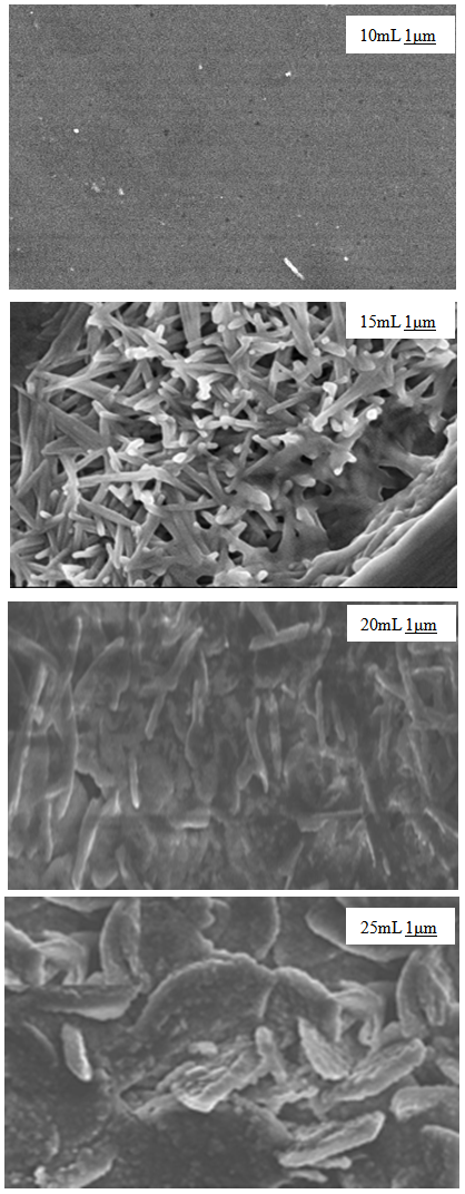 | Figure 2. SEM images of Cd0.5Fe0.5Se thin films deposited by varying the quantity of spray solution |
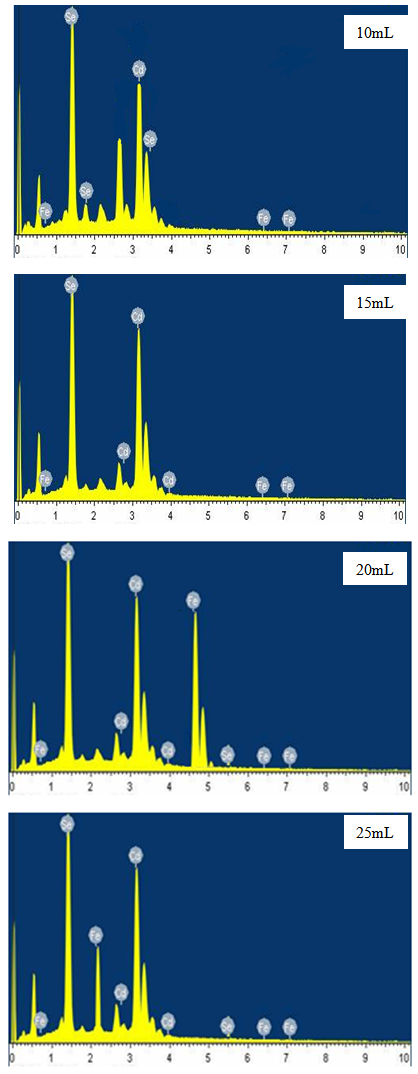 | Figure 3. EDAX spectrum of Cd0.5Fe0.5Se thin films deposited by varying the quantity of spray solution |
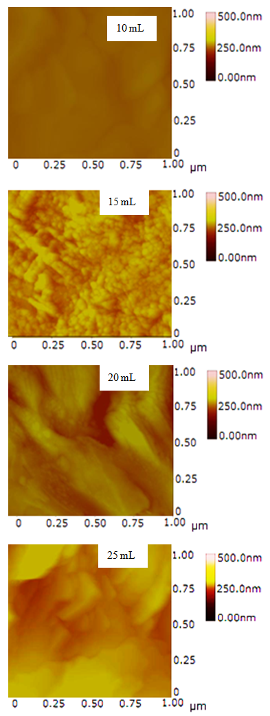 | Figure 4. AFM of Cd0.5Fe0.5Se thin films deposited by varying the quantity of spray solution |
3.3. Electrical Analysis
- Figure 5 shows the IV- characteristics of Cd0.5Fe0.5Se thin films. The linear nature of graph confirms that silver used makes ohmic contact to the film. Also it is observed that, the current flowing through the film at constant applied voltage increases with film thickness, indicating that film conductivity increases with quantity of spray solution. The ‘dc’ electrical resistivity of Cd0.5Fe0.5Se thin film was measured in the temperature range 303–513K by using two-probe method.
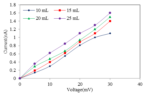 | Figure 5. I-V characteristic of Cd0.5Fe0.5Se thin films deposited by varying the quantity of spray solution |
 | (4) |
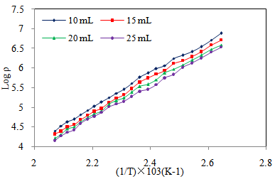 | Figure 6. Variation of Log of resistivity with 1/T of Cd0.5Fe0.5Se thin films deposited by varying the quantity of spray solution |
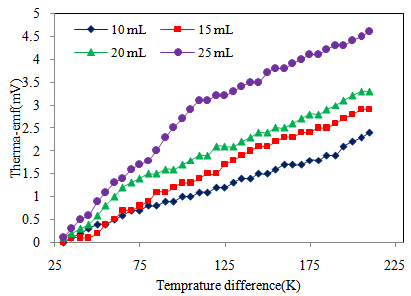 | Figure 7. Variation of thermo emf (mV) with temperature difference of Cd0.5Fe0.5Se thin films deposited by varying the quantity of spray solution |
3.4. Optical Analysis
- The variation of optical absorption with wavelength was analyzed to find the nature of transition involved and to estimate optical band gap. In the present work optical absorption of Cd0.5Fe0.5Se thin film deposited onto glass substrates by varying quantity of spray solution was studied in the wavelength range 350 to 1150 nm. The variation of optical absorption (αt) with wavelength (nm) for Cd0.5Fe0.5Se thin film is shown in figure 8. The nature of transition was determined by using the relation[26],
 | (5) |
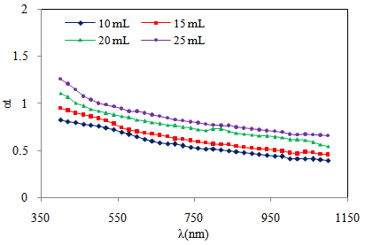 | Figure 8. Variation of optical absorption vs. wavelength of Cd0.5Fe0.5Se thin films deposited by varying the quantity of spray solution |
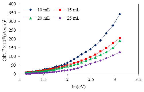 | Figure 9. V The plots of (αhυ)2 vs. hυ of Cd0.5Fe0.5Se thin films deposited by varying the quantity of spray solution |
4. Conclusions
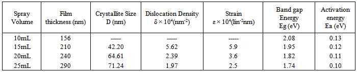
- Porous nanocrystalline Cd0.5Fe0.5Se thin films were successfully spray deposited by varying quantity of spray solution. Structural characterization confirms that Cd0.5Fe0.5Se thin films are nanocrystalline in nature with hexagonal lattice. The crystallite size, dislocation density and strain of the film on the substrate are found to depend on the film thickness. The film morphology is highly influenced by the quantity of spray solution. At 15mL quantity of spray solution, the growth of nano-needle like network is observed which is converted into nano-discs above 15mL. The electrical characterization shows that spray deposited Cd0.5Fe0.5Se thin films are semiconducting in nature with n-type conductivity.
References
| [1] | P. Mandal, R.S. Shrinivasa, S.S. Talwar, S.S. Major, “CdS/ZnS core-shell nanoparticles in arachidic acid LB films”, Appl. Surf. Sci. vol.254, pp.5028-5033, 2008. |
| [2] | V.I. Klimov,“Mechanisms for Photogeneration and Recombination of Multiexcitons in Semiconductor Nanocrystals: Implications for Lasing and Solar Energy Conversion”, J. Phys. Chem. B. vol. 110, pp.16827-16845, 2006. |
| [3] | A.A. Yadav, M.A. Barote, E.U. Masumdar, “A Photoelectrochemical Performance Studies Of CdSe: Sb Electrolyte Cell”, Chalcogenide Lett. vol. 6, No. 4.pp. 149 -153, 2009. |
| [4] | K. Subba, Y.K. Su, S.J. Chang, F.S. Juang, K. Ohdaira, Y. Shiraki, H.P. Liu, I.J. Chen,A.K. Bhatnagar, “Characterization of Cu Doped CdSe Thin Films Deposited by Vacuum Evaporation”, J. Crystal Growth, vol.224, pp.74-82, 2001. |
| [5] | R.Wang, H. Jakobson, R. Kou, J. Tang, R. Fineman, D. Yu, Y. Lu, “Metal and Semiconductor Nanowire Network Thin Films with Hierarchical Pore Structures,”Chem. Mater. vol.18, pp. 4231-4237, 2006. |
| [6] | A.S. Khomane, P.P. Hankare, “Structural, optical and electrical characterization of chemically deposited CdSe thin films”, J. Alloys Comp., vol.489, pp. 605-608, 2009. |
| [7] | L.E. Brus, “Electron–electron and electron‐hole interactions in small semiconductor crystallites: The size dependence of the lowest excited electronic state”, J. Chem. Phys. vol.80, pp. 4403-4409, 1984. |
| [8] | G.A. Ozin, “Nanochemistry - Synthesis in Diminishing Dimensions”, Adv. Mater. vol. 4, pp. 612-648, 1992. |
| [9] | P. Nemec, M. Simurda, I. Nemec, P. Formanek, Y. Nemcova, D. Sprinzl, F. Trojanek, P. Maly, “Chemical bath deposition of CdSe and CdS nanocrystalline films: tailoring of morphology, optical properties and carrier dynamics” , Phys. Status Solidi A, vol. 205, pp. 2324-2329, 2008. |
| [10] | G. Hodes, “Semiconductor and ceramic nanoparticle films deposited by chemical bath deposition”, Phys. Chem. vol.9, pp. 2181- 2196, 2007. |
| [11] | G. Hodes, “Chemical Deposition of Semiconductor Films,” Marcel Dekker, Inc.,Basel, New york,2003. |
| [12] | A. Bhardwaj, E. Varadarajan, P. Srivastava, H.K. Sehgal, “Structural, optical and electrical properties of chemically grown Pb1-xFexSe nanoparticle thin films”, Solid State Comm. vol.146, pp. 53-56, 2008. |
| [13] | X.J. Wu, D.Z. Shen, Z.Z. Zhang, J.Y. Zhang, K.W. Liu, B.H. Li, Y.M. Lu, D.X. Zhao, B.Yao, “p-type conductivity and donor-acceptor pair emission in Cd1−xFexS dilute magnetic semiconductors”, Appl. Phys. Lett. Vol.89, pp. 262118, 2006. |
| [14] | K. Liua, b, J.Y. Zhang, Xiaojie Wua, Binghui Li, Bingsheng Li, Youming Lu, Xiwu Fan, Dezhen Shen, “Fe-doped and (Zn, Fe) co-doped CdS films: Could the Zn doping affect the concentration of Fe2+ and the optical properties”, Physica B. vol. 389, pp.248-251, 2007. |
| [15] | A. U. Ubale, S. G. Ibrahim, “Structural, Electrical and Optical Properties of Nanostructured FeCdS3 Thin Films Deposited by Chemical Spray Technique: Effect of Complex”, Mater. Chem. Phy. vol. 2, pp. 57-64, 2012. |
| [16] | A. U. Ubale, S. G. Ibrahim, “Effect of acetic acid complex on physical properties of nanostructured spray deposited FeCdS3 thin films”, J. Alloys Comp., vol.509, pp.2364- 2367, 2011. |
| [17] | S.M. Pawar, A.V. Moholkar, K.Y. Rajpure, C.H. Bhosale, “Photoelectrochemical investigations on electrochemically deposited CdSe and Fe-doped CdSe thin films”, Sol. Energy Mater., vol. 92, pp. 45-49, 2008. |
| [18] | K.Y. Rajpure, P.A. Anarase, C.D. Lokhande, and C.H. Bhosale, “Photoelectrochemical studies on electrodeposited Cd-Fe-Se thin films”, phys. stat. sol. (a), vol.172, pp. 415-423, 1999. |
| [19] | A.U. Ubale, V.P. Deshpande, “Effect of manganese inclusion on structural, optical and electrical properties of ZnO thin films”, J.Alloys Comp.vol. 500, pp. 138-143, 2010. |
| [20] | S.M. Pawar, A.V. Moholkar, K.Y. Rajpure, C.H. Bhosale,“Electrosynthesis and characterization of Fe doped CdSe thin films from ethylene glycol bath”, Appl. Surf. Sci. vol.253, pp. 7313-7317, 2007. |
| [21] | S. Senthilarasu, Y.B. Hahn, Soo-Hyoung Lee, “Structural analysis of zinc phthalocyanine (ZnPc) thin films: X-ray diffraction study”, J. Appl. Phys. Vol.102, pp. 043512, 2007. |
| [22] | A. Chowdhury, B. Biswas, M. Majumder, M. K. Sanyal, B. Mallik, “Studies on Phase Transformation and Molecular Orientation in Nanostructured Zinc Phthalocyanine Thin Films Annealed at Different Temperatures”, Thin Solid Films, vol.520, pp. 6695-6704, 2012. |
| [23] | Dipalee J. Desale, Shaheed Shaikh, Arindam Ghosh, Ravikiran Birajadar, Farha Siddiqui, Anil Ghule, Ramphal B.Sharma, “Preparation and characterization of CdS–Bi2S3 nanocomposite thin film by successive ionic layer adsorption and reaction (SILAR) method”, Composites: Part B , vol.43, pp. 1095–1100, 2012. |
| [24] | Y. S. Sakhare, A. U. Ubale, “Optical properties of FeSe thin films deposited by chemical bath deposition technique: Effect of molar concentration of Fe (NO3)3.9H2O”, Arch. Phy. Res., vol.3, pp. 452-458, 2012. |
| [25] | S.S. Kale, C.D. Lokhande, “Thickness-dependent properties of chemically deposited CdSe thin films”, Mater. Chem. Phy. vol. 62, pp. 103-108, 2000. |
| [26] | Durgajanani Sivalingam, Jeyaprakash Beri Gopalakrishnan, John Bosco Balaguru Rayappan, “Structural, morphological, electrical and vapour sensing properties of Mn doped nanostructured ZnO thin films,”Sens. Actu. B. vol. 166– 167, pp. 624–631, 2012. |