Ashok U. Ubale, V.N. Mitkari, D. M. Choudhari, J
Nanostructured Thin film Materials Laboratory, Departments of Physics, Govt. Vidarbha Institute Sciencesand Humanities, Amravati 444604, Maharashtra, India
Correspondence to: Ashok U. Ubale, Nanostructured Thin film Materials Laboratory, Departments of Physics, Govt. Vidarbha Institute Sciencesand Humanities, Amravati 444604, Maharashtra, India.
| Email: |  |
Copyright © 2012 Scientific & Academic Publishing. All Rights Reserved.
Abstract
Metal chalcogenide thin film preparation by chemical bath deposition is currently attracting considerable attention as it is relatively less expensive, simple and convenient method for large area deposition. In the present work preparation of un-doped and Cu doped As2S3 thin films by chemical bath deposition method is reported. The film characterization is undertaken to study structural, optical and electrical properties of As2S3 and Cu:As2S3 thin films. The structural characterization shows mixed monoclinic and hexagonal lattice due to As2S3 and CuS.The electrical resistivity of the As2S3 film decreases with doping as it introduces the impurity donor level in As2S3. The activation energy and optical band gap decreases from 0.26 to 0.03 eV and 3 to 2.34 eV due to doping of Cu in As2S3 film respectively. The thermo-emf measurement confirms the n-type conductivity.
Keywords:
Chemical Synthesis, Nanostructured Thin Films, Electrical, Optical , Structural Properties
Cite this paper: Ashok U. Ubale, V.N. Mitkari, D. M. Choudhari, J, Synthesis of Nanostructured Cu:As2S3 Thin Films by Chemical Bath Deposition Method and Their Physical Properties, International Journal of Materials and Chemistry, Vol. 3 No. 2, 2013, pp. 33-38. doi: 10.5923/j.ijmc.20130302.03.
1. Introduction
The industrial development of nanoscience and nanotechnology needs synthetic materials of tailor made properties that arise with decreasing size of nanomaterial having a higher packing density, higher speed performance with lower cost[1,2]. Thin films have potential applications in many devices such as solar selective coatings, as a storage electrode in photoelectrochemical storage devices, photoconductors, IR detectors and solar cells etc. With rapid technological advances in the preparation of films with controlled, reproducible and well defined structures, thin films are expected to play increasingly important role in the studies of a variety of solid state phenomena. The properties of large verity of new and interesting materials obtained by thin film techniques will undoubtedly draw considerable attention in future[3]. The advanced microelectronics based on surface engineering needs well developed deposition processes, as the most demanding approaches in the near future. New concepts and design methodologies are needed to synthesize new thin film devices and to integrate them for various operations. Arsenic trisulfide (As2S3) is a technically important material because of its good transparency in the 0.7-11-µm wavelength range and excellent resistance against diversification, moisture, and corrosion. It is well known that As2S3 has variety of applications in optical imaging, hologram recording and recently in various electronic devices, including electro-optic information storage devices and optical mass memories[4-8]. Various methods have been employed to deposit As2S3 thin films. Pawar et al[9] have prepared As2S3 films by solution gas interface technique. Hajto et al.[10] have reported physical properties of spin-coated As2S3 films. Lokhande[11] has reported solution growth of As2S3 films using As2O3 and Na2S2O3 as As3+and S2- ion sources, respectively, from complexed (with EDTA) acidic and alkaline aqueous baths. Desai and Lokhande[12] have deposited As2S3 films onto glass substrates from an acidic sodium thiosulphate bath, using disodium salt of ethylenediaminetetraacetic acid to complex As3+ ions. The films were amorphous, with an optical band-gap of 2.36 eV and resistivity of the order of 106 Ω-cm. Deshmukh et al[13] have prepared As2S3 thin films in a non-aqueous medium (methanolic solution) using simple chemical deposition process. Mane et al[14] have deposited nanocrystalline As2S3 thin films in aqueous medium at low temperature by using chemical bath deposition technique. In this manuscript preparation of As2S3 and Cu:As2S3 thin films by using chemical bath deposition method are reported. These films are characterized by XRD, SEM, electrical resistivity and optical absorption measurements to investigate their physical properties.
2. Experimental
Chemical bath deposition is well suited for producing nanostructured thin films suitable for solar energy related applications. The films are deposited on substrates immersed in dilute solutions containing metal and sulfide ions. In the present work nanostructured As2S3 and Cu: As2S3 thin films were prepared by using chemical bath deposition method. For deposition of As2S3 films, 60 ml 0.5 M As2O3 solution is mixed with 60 ml 0.5 M tartaric acid. Then, 60ml 0.5 M sodium thiosulphate is added in it with constant stirring. The colour of mixture changes from pale yellow to dark yellow after about 30 minute. The well deposited shining yellow coloured As2S3 thin films were removed from the solution after 6 h deposition time and used for further characterization. The as-deposited As2S3 films are designated as ‘Film A’ in the further discussion. In the present work Cu doping in As2S3 is achieved by two different ways. In the first method, the as-deposited As2S3 thin films are heated in 0.5 M cupric acetate solution for 3 h at 60° C. The as-deposited As2S3 films were yellow in colour and after heating in cupric acetate bath the film colour become golden yellow. This confirms the addition or replacement of some Cu atoms in As2S3. The Cu: As2S3 films prepared by this method are designated as ‘Film B’ in the further discussion. In second method to prepare Cu: As2S3 films, 5 ml 0.5 M cupric acetate solution is directly mixed in the reaction mixture during deposition of As2S3 thin films. The solution colour becomes golden yellow after about 40 minute. The well deposited uniform Cu: As2S3 films were removed from the reaction beaker after 6 h deposition time. These films are designated as ‘Film C’ in the further discussion. Thickness (t) of the film is defined as the distance perpendicular to surface from a point on the boundary surface through the film to other boundary surface. Amongst the different methods for measuring the thickness the weight difference method is simple and convenient. The mass of the deposited film is related to area and density of the material as, | (1) |
Where, t is the thickness of the film, m is mass of the deposited sample, A is area of the deposited sample and ρ is the density of the deposited sample.The two point dc probe method of dark electrical resistivity was used to study the variation of resistivity with temperature. The film of size 1 cm2 on the glass substrate was used. Silver paste was used to make ohmic contacts. A brass block was used as sample holder cum heater. A thermocouple with DPM was used for temperature measurement along with nanometer for current measurement. The variation of absorption density ‘αt’ with the wavelength for As2S3 and Cu:As2S3 film was carried out using double beam spectrophotometer, ELICO - SL164-SP2 in the wavelength range between 350 to 890 nm. The thermo emf measurements were carried to find the type of conductivity. The crystallographic studies of thin films were characterized by using a PANalyticalX’Pert PRO MRD X-ray diffractometer with CuKα radiation in the 2Ɵ range from 20 to 80 degree. Also the film microstructure was studied by using JOEL’s JSM -7600F scanning electron microscope with 1 nm resolution.
3. Results and Discussion
3.1. Reaction Mechanism
The As2S3 and Cu:As2S3films were prepared in the presence of complexing agenttartaric acid. The metal ions produces complex in the solutions, which dissociates slowly to release them for further process. The precipitate formation in the solution takes place when the ionic product (I.P) exceeds the solubility product (S.P). In aqueous solution Na2S2O3 dissociates as, | (2) |
Na2S2O3is a reducing agent by virtue of half-cell reaction, | (3) |
In acidic medium dissociation of  takes place as,
 | (4) |
The electrons released in equation 3 react with S as, | (5) |
The tartarate ion forms complex with arsenic, which further reacts with S2- to give As2S3 thin film as, | (6) |
 | (7) |
In order to dope Cu in As2S3, the as deposited film is heated in 0.5 M cupric acetate solution for 3 h at 60° C. The yellow coloured As2S3 film becomes golden yellow indicating addition of Cu in As2S3. However in second method the 5ml 0.5 M cupric acetate solution is directly mixed in deposition bath to deposit Cu: As2S3 films. The thickness of un-doped As2S3 film is 217 nm. When this film is heated in cupric acetate bath, film thickness decreases to 205 nm. The fraction of As2S3 film may be dissolved in cupric acetate bath due to heating in it for 3 h. However, the Cu: As2S3 film deposited by adding cupric acetate directly in reaction bath has thickness 288 nm.
3.2.Structural Properties
Fig.1 shows XRD patterns of As2S3 and Cu: As2S3 films. The diffraction peaks observed in the XRD pattern corresponds to monoclinic As2S3 and hexagonal covellite CuS lattice. The observed XRD data is in good agreement with standard data (Table 1). The (301) orientation due to As2S3 is repeated in both As2S3 and Cu: As2S3 film. The (310), (320) and (411) orientations due to monoclinic As2S3 and (207) orientation due to hexagonal CuS is repeated in both Cu: As2S3 thin films deposited by post heating of As2S3film in cupric acetate source and by direct addition of cupric acetate in deposition bath. The average crystallite size was determined from diffraction peaks using the Scherrer formula, d= (0.9 λ)/β Cosθ, where λ is wavelength used (0.154 nm); β is angular line width at half maximum intensity in radians; θ is Bragg’s angle. The grain size of As2S3 is 15 nm and it becomes to 11 and 13nm for Cu: As2S3 thin films deposited by post heating of As2S3 film in cupric acetate and by direct addition of cupric acetate in deposition bath. | Figure 1. XRD pattern of doped and un-doped As2S3 films: (A) As2S3, (B) Cu: As2S3 film in which Cu is added by post heating of As2S3 film in Cu source and (C) Cu: As2S3, in which Cu is added during deposition process |
3.3. SEM Studies
Figure 2 shows the SEM images of As2S3 and Cu: As2S3 thin films. The SEM image of as deposited As2S3 film shows random distribution of spherical grains covering whole substrate surface. At some places the substrate surface is quite rough indicating porous nature of film. However, the SEM image of Cu: As2S3 obtained by heating as deposited As2S3 film in Cu source shows growth of some wafer like disc-shaped crystals of CuS on the homogenous surface. It should be noted that while heating some amount of As2S3 may be dissolved in the bath that makes the film surface smoother as seen in SEM. While the SEM of Cu: As2S3 film deposited by mixing cupric acetate directly in reaction bath during deposition shows grain growth with better mixing of Cu in As2S3 .
3.4. Electrical Properties
To investigate electrical properties of the films silver paste is applied for making ohmic contacts. The existence of barrier is usually observed when contact is made between metal and semiconductor because of either improper matching of their work function or the presence of surface states on the semiconductor[4, 5]. The nature of contact was checked by using two probe method. The I-V characteristic of As2S3/Ag and Cu: As2S3/Ag is shown in figure 3. The I-V characteristics is found to be linear within the voltage range up to 30 V and shows that silver electrode produces ohmic contacts with As2S3 and Cu: As2S3. Also it was observed that Cu: As2S3 films deposited by direct mixing of cupric acetate in deposition bath are more conductive.Table 1. Comparison of XRD data of AsS3 and Cu: As2S3thin films
 |
| |
|
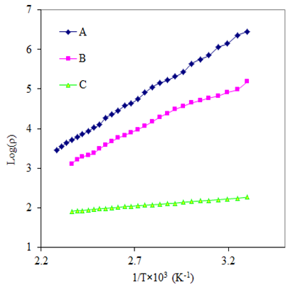
The resistivity of thin films was studied by using two point dc probe method in the temperature range 303 to 438 K. Fig 4 shows the variation of resistivity (log ρ) with reciprocal of temperature (1/T)×103 for As2S3 and Cu: As2S3 films. It was observed that the resistivity of As2S3 at 303K temperature is 2.8×10⁶ Ω-cm and it decreases to 1.5×10⁵ Ω-cm for Cu: As2S3 deposited by heating As2S3 in Cu source and becomes 1.8 ×10² Ω-cm for Cu: As2S3 deposited by adding Cu source directly in deposition bath. This decrease in resistivity is due to Cu-doping. The addition of Cu may increase the donor states in As2S3, which enhances the conductivity. Also the electrical resistivity decreases with temperature indicating semiconductors nature of the film.The electrical resistivity follows the relation, | (8) |
Where  is the resistivity at temperature T,
  is a constant, K is Boltzmann’s constant and E0 is activation energy required for conduction. The activation energy for As2S3 decreases from0.26 to 0.18eV due to Cu doping in As2S3 by first method and becomes 0.03eV for Cu: As2S3 film deposited by adding Cu source directly in deposition bath. It may be due to decrease in resistivity with Cu doping. Addition Cu in As2S3 may increase the donor i.e. trap levels in the band structure.
 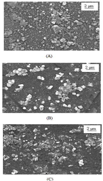 | Figure 2. SEM images of doped and un-doped As2S3 films: (A) As2S3, (B) Cu: As2S3 film Cu is added by post heating of As2S3 film in Cu source and (C) Cu: As2S3, Cu is added during deposition process |
 | Figure 3. IV characteristics of doped and un-doped As2S3 films: (A) As2S3, (B) Cu: As2S3 film in which Cu is added by post heating of As2S3 film in Cu source and (C) Cu: As2S3, in which Cu is added during deposition process |
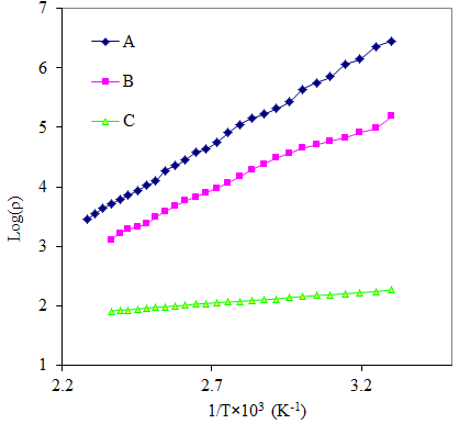 | Figure 4. Variation of log of electrical resistivity with reciprocal of temperature of doped and un-doped As2S3 films: (A) As2S3, (B) Cu: As2S3 film in which Cu is added by post heating of As2S3 film in Cu source and (C) Cu: As2S3, in which Cu is added during deposition process |
The TEP measurement is used to determine the type of conductivity of thin film. Temperature difference between two ends of semiconductor causes a transport of carriers from hot to cold end creating an electric field which gives rise to thermo-emf. The polarity of the thermally generated voltage at hot end was positive, indicating that the As2S3 and Cu:As2S3 films are of n-type. Fig. 5 shows that the thermo-emf generated across the film increase with applied temperature differenceacross the film. The rise in thermo-emf in doped film is attributed to the increase in carrier concentration and mobility.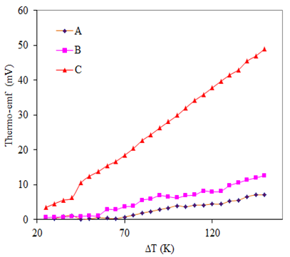 | Figure 5. Variation of thermo-emf with temperature difference applied across doped and un-doped As2S3 films: (A) As2S3, (B) Cu: As2S3 film in which Cu is added by post heating of As2S3 film in Cu source and (C) Cu: As2S3, in which Cu is added during deposition process |
3.5. Optical Properties
The study of materials by means of optical absorption provides a simple method for explaining some features concerning band structure of materials. In the present investigation optical absorption of As2S3 and Cu:As2S3films was studied in the wavelength range of 350 to 890 nm. The variation of absorbance  with wavelength (nm) for As2S3 and Cu: As2S3 is shown in figure 6.The absorption for As2S3 film is quite small as compared to Cu:As2S3 films. The nature of the transition (direct or indirect) is determined by using the relation[15],
 | (9) |
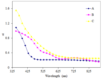 | Figure 6. Variation of optical absorption with wavelength for doped and un-doped As2S3 films: (A) As2S3, (B) Cu: As2S3 film in which Cu is added by post heating of As2S3 film in Cu source and (C) Cu: As2S3, in which Cu is added during deposition process |
 | Figure 7. Variation of (αhν)2 vshν for doped and un-doped As2S3 films: (A) As2S3, (B) Cu: As2S3 film in which Cu is added by post heating of As2S3 film in Cu source and (C) Cu: As2S3, in which Cu is added during deposition process |
Where A is constant, hυ is photon energy and Eg is the optical band gap. The exponent n depends on the nature of the transition, n=1/2, 2, 3/2 or 3 for allowed direct, allowed indirect, forbidden direct or forbidden indirect transitions, respectively. The plots of (αhν)2 versus hν are shown in Fig.7 for As2S3 and Cu: As2S3 films. The nature of the plots indicates the existence of direct transition. The band gap energy Eg is determined by extrapolation the straight portion of the plot to the energy axis. The band gap energy of as deposited As2S3 film is 3 eV and Cu: As2S3 film prepared by post heating of As2S3 film in Cu source is 2.34eV and becomes 2.84 eV when Cu is doped during deposition .
4. Conclusions
In the present work Cu doped and un-doped As2S3 thin films are prepared by using CBD method. The structural, electrical and optical properties of As2S3 and Cu As2S3 thin films are studied. The I-V-characteristics of these films is almost linear indicating ohmic contact between Ag and film. Electrical resistivity measurement indicates semiconducting nature of As2S3 and Cu: As2S3 films. The resistivity decreases with Cu doping as it increases the impurity donor levels in As2S3. The activation energy decreases from 0.26 to 0.03 eV due to addition of Cu in As2S3. It was found that the band gap energy is decreased from 3 eV to 2.34 eV due to doping of Cu in As2S3.
ACKNOWLEDGEMENTS
The authors are thankful to University Grants Commission, for financial support under the project (No: F.47-1695/10 dated 16/3/2011).
References
| [1] | J. Schoonman, “Nanostructured materials in solid state ionics”,Solid State Ionics, vol. 135, pp. 5-19, 2000. |
| [2] | L. I. Maissel and R. Gilana, “Hand Book of thin film technology”, Mc. Grow Hill, New York (1970). |
| [3] | K. L. Chopra in “Thin film phenomena”, Mc. Graw Hill, New York, (1969). |
| [4] | H. Rawson, “Inorganic Glass Forming System, Nonmetallic Solids”, Academic Press, New York, 1967. |
| [5] | T. Kawaguchi1, S. Maruno1 and S. R. Elliott,“Effect of addition of Au on the physical, electrical and optical properties of bulk glassy As2S3”, J. Appl. Phys.,vol. 80, pp. 5625-5633, 1996. |
| [6] | K. Tanaka, “Effect OfUv Exposure On Optical Properties in Intermolecular Distance in Amorphous As2S3 Network”, Appl. Phys. Lett., vol. 26, pp 243-245, 1975. |
| [7] | K.Tanaka and Y. Ohtsuka, “Composition dependence of photo-induced refractive index changes in amorphous AsS films”, Thin Solid Films, vol. 57, pp. 59-64, 1979. |
| [8] | V. A.Danko, I. Z.Indutnyi, A. A.Kudryavstev and V. I. Minko, “Photodoping in As2S3:Ag thin films”, Phys. Status Solidi, vol. 124, pp. 235-242, 1991. |
| [9] | S. H. Pawar, S.P.Tamhankar, P. N. Bhosale and M. D. Uplane, “Growth of Sb2S3 Films by Solution-Gas Interface Technique”, Ind. J. Pure Appl. Phys., vol. 21, pp. 665, 1983. |
| [10] | E. Hajto, P. J. S. Ewen, R. Belford, J. Hajto and A. E. Owen, “Optical properties of spin-coated amorphous chalcogenide thin films”, J. Non-Cryst. Solids, vol. 97-98, pp. 1191-1194, 1987. |
| [11] | C. D. Lokhande, “Solution growth of As2S3 and Sb2S3 thin films”, Ind. J. Pure Appl. Phys., vol. 29, pp. 300-302, 1991. |
| [12] | J. D. Desai and C. D. Lokhande, “Preparation and characterization of As2S3 thin films”, Ind. J. Pure Appl. Phys., vol. 33, pp. 247-247, 1995. |
| [13] | L.P.Deshmukh, J. S.Dargad, and C.B. Rotti, , “Preparation and characterization of As2S3 thin films deposited by CBD”, Ind. J. Pure Appl. Phys., vol. 33, pp. 687, 1995. |
| [14] | R.S.Mane, C.D. Lokhande and M. D. Uplane, “Chemical deposition and characterization of silver films”, Ind. J. Pure Appl. Phys., vol. 33, pp. 693-699, 1995 |
| [15] | A. U. Ubale, “Effect of complexing agent on growth process and properties of nanostructured Bi2S3 thin films deposited by chemical bath deposition method”, Mater. Chem. Phys., vol. 12, pp. 555–560, 2010. |
 Abstract
 Reference
 Full-Text PDF
 Full-text HTML