-
Paper Information
- Next Paper
- Previous Paper
- Paper Submission
-
Journal Information
- About This Journal
- Editorial Board
- Current Issue
- Archive
- Author Guidelines
- Contact Us
International Journal of Materials and Chemistry
p-ISSN: 2166-5346 e-ISSN: 2166-5354
2013; 3(2): 28-33
doi:10.5923/j.ijmc.20130302.02
Characterization of Nanocrystalline CdS Thin Films Prepared by Thermal Evaporation
 Abstract
 Reference
 Full-Text PDF
 Full-text HTML
Shadia J. Ikhmayies
Al Isra University, Faculty of Information Technology, Department of Basic Sciences-Physics, Amman, 16197, Jordan
Correspondence to: Shadia J. Ikhmayies, Al Isra University, Faculty of Information Technology, Department of Basic Sciences-Physics, Amman, 16197, Jordan.
| Email: |  |
Copyright © 2012 Scientific & Academic Publishing. All Rights Reserved.
Nanocrystalline CdSthin films were prepared by thermal evaporation on glass substrates at ambient temperature. The films were characterized by recording and analyzing their transmittance, X-ray diffraction (XRD) patterns, scanning electron microscope (SEM) images and Energy dispersive X-ray (EDAX) spectra. X-ray diffractograms revealed that the material is nanocrystalline with predominant cubic crystal structure and preferential orientation along (111) plane. SEM micrographs confirmed the nanostructure of the material and showed uniform and well covered surfaces. EDAX reports revealed that the films are cadmium rich and contain oxygen. The first derivative of the absorbance was used to estimate the effective bandgap energies of the nanocrystallites and the hyperbolic band model was used to estimate their radii. The results were compared with those obtained by XRD and SEM measurements.
Keywords: II-VI Semiconductors, CdS/CdTe Solar Cells, Heterojunctions, Nanocrystallites, Thin Films
Cite this paper: Shadia J. Ikhmayies, Characterization of Nanocrystalline CdS Thin Films Prepared by Thermal Evaporation, International Journal of Materials and Chemistry, Vol. 3 No. 2, 2013, pp. 28-33. doi: 10.5923/j.ijmc.20130302.02.
Article Outline
1. Introduction
- CdS thin films are of considerable interest as they can be used in fabrication of solar cells and other opto-electronic devices. In particular, heterojunction solar cells with a narrow band gap base and wide band gap window have been investigated in an attempt to develop efficient, stable and low-cost solar cells[1]. The CdS quantum dot embedded in a glass matrix is one of the well-known quantum dot systems and its electronic and luminescent properties have been studied extensively[2].Three-dimensional confinement of carriers within the quantum dots leads to the blue shift of the optical band-gap and to modification of many properties of semiconductor material[3]. It has been argued that in these semiconductor nanoparticles the hyperbolic band model gives a better fit to the observed quantum size effect as compared to the effective mass approximation[4].There are different ways to synthesize CdS nanoparticles such as colloidal particulates[5], chemical deposition[6], sol-gel[7], spray pyrolysis[8], chemical bath deposition[3], thermal evaporation[9], etc. In the present work, thermal evaporation technique has been chosen for the deposition of nanocrystalline CdS thin films as it is simple compared with other new and sophisticated techniques[10].Most studied nanocrystalline semiconductors belong to the II-VI group as they are relatively easy to synthesize and generally prepared as particulates or in thin film form. Among II-VI compounds, CdS is one of the most studied materials. For example, Němec et al.[3] reported on the control of nanocrystal sizes in CdS nanocrystalline films prepared by ammonia-free chemical bath deposition technique. Datta et al.[11] achieved size tunability of thiophenol capped CdS nanoparticles (NPs) by controlling the temperatures at the time of synthesis. In this work CdS nanocrystallites were produced by thermal evaporation on glass substrates at ambient temperature. A narrow range of nancrystallites' size was obtained as seen from the results deduced from the XRD diffractograms, SEM micrographs and first derivative with the hyperbolic model. It was found that narrower range of crystalline size could be obtained at lower values of film thickness.
2. Experimental Part
- Undoped CdS thin films were deposited by thermal evaporation at ambient temperature on glass substrates of dimensions (6×2.6×0.1cm3) in a high vacuum system (~10-5 mbar) provided with a Turboe pump. The evaporation rate was about 10 Å/s and it was measured by a cooled quartz crystal monitor. The distance between the source and the substrate was about 30 cm. Films of thickness 50-495 nm were produced through different individual evaporations.The transmittance of the films was measured by using a double beam Shimadzu UV 1601 (PC) spectrophotometer with respect to a piece of glass similar to the substrates in the wavelength range 300-1100 nm. The thickness of the films was estimated from the interference maxima and minima in the transmittance by using the method of Alvin[12]. X-ray measurements were recorded by a Philips PW1840 Compact X-ray diffractometer system with Cu Kα (λ = 1.5405 Å). The SEM micrographs were taken by a FEI scanning electron microscope (Inspect F 50), which was supplied by energy dispersive analysis by X-rays (EDAX), so the compositional analysis of the films was performed by the same system.
3. Results and Discussion
- Fig.1 displays the X-ray diffractograms of two CdS films with different thickness. As the figure shows, the structure is mainly identified as zinc blende, where the characteristic lines of the cubic phase C(1 1 1), C(2 2 0), C(3 1 1) and C(2 2 2) are evident in the diffractogram. The C(1 1 1) peak at 2θ about 26.2° is overlapped by a broad band produced by the amorphous glass substrate. Nĕmec et. al.[3] says that cadmium sulfide nanocrystallites tend to crystallize in cubic (zinc-blende) structure unlike the bulk CdS which is usually hexagonal (wurtzite). But the diffractogram also shows some lines of the hexagonal phase, which are the H(1 0 0), H(1 0 1) and the H(0 0 2) lines. On the other hand it is known that the peak produced by the C(1 1 1) crystalline planes of the cubic CdS and that of the H(0 0 2) crystalline planes of the hexagonal structure coincide within 1 per cent. As the figure shows, the C(1 1 1) is the preferential orientation for crystal growth, but it is stronger and narrower in the case of the 300 nm film, indicating that the grain size in this film is larger.The grain size was calculated by using Scherrer formula and the line C(1 1 1) in the XRD pattern of the film with thickness 300 nm, where it has the largest intensity.
 | (1) |
 is the grain size (diameter of the nanocrystallites),
  is the X-ray wavelength used,
  is the angular line width of the half-maximum intensity and
  is Bragg angle. The grain size was found to be about 15 nm for the crystallites grown in this direction, or the average radius of the nanocrystallites is about 7.5 nm. It is necessary to remind by the fact that, lines of smaller intensity give smaller values of in both films.
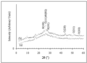 | Figure 1. X-ray diffractogram of thermally evaporated CdS thin films of thickness a) 100 nm. b) 300 nm |
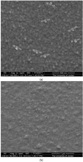 | Figure 2. SEM micrographs of thermally evaporated CdS thin films with thickness a) t = 400 nm. b) t = 100 nm |
 | (2) |
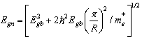
 is the bandgap for the bulk semiconductor which equals to 2.42 eV[15], is the particle's radius, and
  is the effective electron mass. Taking
  [16] for CdS, where is the mass of a free electron. The calculated values of particle's radii for the two aforementioned films are displayed in tables 1 and 2.
 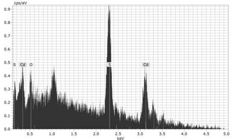 | Figure 3. The EDAX pattern for the thermally evaporated CdS film of thickness 100 nm. |
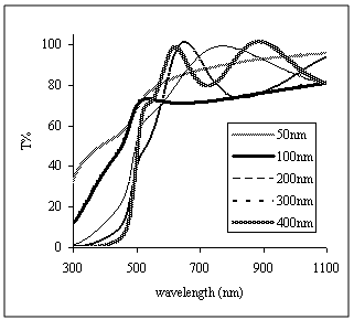 | Figure 4. Transmittance curves of vacuum evaporated CdS thin films of different values of film thickness |
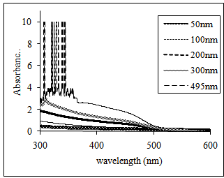 | Figure 5. The absorbance curves of vacuum evaporated CdS thin films of different values of film thicknessssssssssssss |
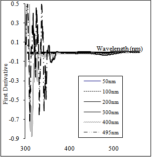 | Figure 6. The first derivative of the absorbance curves of CdS thin films of different thickness |
|
4. Conclusions
- Nanocrystalline cadmium sulfide CdS thin films were produced by thermal evaporation on glass substrates at ambient temperature. The films were characterized by recording their XRD diffractograms, SEM observations, EDAX spectra and transmittance measurements. XRD diffractograms and SEM micrographs revealed the nano-crystalline nature of the films. EDAX spectra showed that the films are cadmium rich and that they contain oxygen. The transmittance and absorbance curves confirmed the presence of quantum dots. The bandgap energy for the different nanocrystallites
 was estimated from the first derivative of the absorbance. These values of bandgap energy were used to calculate the paticles' sizes according to the hyperbolic model. The estimated values of the optical band gap are found to be 2.594-4.113 eV, corresponding to nanocrystallites of radii 11.4-3.2 for CdS film of thickness 300 and 400 nm. These results are compared with the results obtained by XRD diffractograms and SEM images.
 ACKNOWLEDGEMENTS
- I would like to thank Sameer Farrash from the physics department in the University of Jordan for producing the films by thermal evaporation. Also I want to thank Waddah Fares Mahmoud and Azzam Karadsheh from the department of geology in the University of Jordan for taking the SEM micrographs and for taking XRD diffractograms respectively.
References
| [1] | M. Singh, Y. K. Vijay, and B. K. Sharma, A variable electron beam and its irradiation effect on optical and electrical properties of CdS thin films, PRAMANA- journal of physics, 69 (4) (2007), 631–638. |
| [2] | A. Ates, M. A. Yildirim, M. Kundakçi, and M. Yildirim, Investigation of Optical and Structural Properties of CdS Thin Films, Chinese Journal of Physics 45 (2-I) (2007), 135-141. |
| [3] | P. Nĕmec, I. Nĕmec, P. Nahálková, K. Knížek, P. Malý, Ammonia-free chemical bath deposition of CdS films: tailoring, the nanocrystal sizes, Journal of Crystal Growth 240 (2002), 484–488. |
| [4] | K. K. Nanda, S. N. Sarangi, S. N. Sahu, S.K. Deb, S.N. Behera, Raman spectroscopy of CdS nanocrystalline semiconductors, Physica B 262 (1999), 31-39. |
| [5] | V. L. Colvin, A. P. Alivisatos, J. G. Tobin, Valence-Band photoemission from a quantum-dot system, Physical Review Letters, 66 (21) ( 1991), 2786-2789. |
| [6] | R. S. Singh, and S. Bhushan, Structural and optical properties of chemically deposited Cd(S–Se): CdCl2, Sm films, Bull. Mater. Sci., 32 (2) (2009), 125–133. |
| [7] | Jialong Zhao, Kai Dou, Shaozhe Lu, Yinmin Chen, Shihua Huang, Jiaqi Yu, Weidong Xiang, Zishang Ding, Photoluminescence of CdS semiconductor nanocrystals in sodium borosilicate glasses, Journal of Materials Science Letters 15 (1996), 702-705. |
| [8] | I. K. Battisha, H. H. Afify, G. Abd El Fattah and Y. Badr, "Raman and photoluminescence studies of pure and Sn-enriched thin films of CdS prepared by spray pyrolysis", FIZIKA A 11 (1) (2002), 31-42. |
| [9] | P. P. Sahay, R. K. Nath, and S. Tewari, Optical properties of thermally evaporated CdS thin films, Cryst. Res. Technol. 42 (3) (2007), 275 – 280. |
| [10] | Shadia J Ikhmayies and Riyad N Ahmad-Bitar, Optical properties of nanocrystalline CdTe thin films, Physica B 405 (2010), 3141–3144. |
| [11] | A. Datta, A. Priyam, S.N. Bhattacharyya, K.K. Mukherjea, A. Saha, Temperature tunability of size in CdS nanoparticles and size dependent photocatalytic degradation of nitroaromatics, Journal of Colloid and Interface Science 322 (2008), 128–135. |
| [12] | Goodman M. Alvin, Optical interference method for the approximate determination of refractive index and thickness of a transparent layer. Applied Optics 17 (17) (1978), 2779-2787. |
| [13] | K. K. Nanda, S. N. Sarangi, S. Mohanty and S. N. Sahu. Optical properties of CdS nanocrystalline films prepared by a precipitation technique, Thin Solid Films 322 (1998),21-27. |
| [14] | Gary Hodes, Ana Albu-Yaron, Franco Decker and Paulo Motisuke, Three-dimensional quantum-size effect in chemically deposited cadmium selenide films, Physical Review B, 36 (8) (1987), 4215-4221. |
| [15] | Ziaul Raza Khan, M. Zulfequar, Mohd. Shahid Khan, Chemical synthesis of CdS nanoparticles and their optical, and dielectric studies, J. Mater Sci 46 (2011), 5412–5416. |
| [16] | M. Bedir, M. Öztas, Ö. f. Bakkaloğlu and R.Ormanci, Investigations on structural, optical and electrical parameters of spray deposited ZnSe thin films with different substrate temperature, Eur.Phys.J.B., 45 (2005), 465-471. |