International Journal of Materials and Chemistry

p-ISSN: 2166-5346    e-ISSN: 2166-5354

2012;  2(5): 197-204

doi: 10.5923/j.ijmc.20120205.03

Influences of γ–Radiation and Surfactants on Electrical and Magnetic Properties of Cu0.1Zn0.9Mn2O4 Nanoparticles

M. Khairy, M. A. Mousa

Chemistry Department, Faculty of Science, Benha University, Egypt

Correspondence to: M. Khairy, Chemistry Department, Faculty of Science, Benha University, Egypt.

Email:

Copyright © 2012 Scientific & Academic Publishing. All Rights Reserved.

Abstract

Nanosized Cu0.1Zn0.9Mn2O4 were prepared by hydrothermal method in absence and presence of surfactants. The samples were characterized using XRD, SEM and TEM. All samples showed spinel crystal structure with crystallite sizes depending on the preparation method and lay in the range of 17-89 nm. Electrical conductivity as a function of frequency and temperature has been studied. The conductivity results showed that all investigated samples behave like semiconductors and could be explained by hopping mechanism in which the conduction occurres via electron exchange amongst Mn+ and Mn+1 ions situated on octahedral sites in spinel lattice. Room temperature magnetic properties using VSM were studied. Effect of γ-radiation on the studied properties is investigated. Each of particle size, morphology, magnetic and electrical properties is affected with each of the type of surfactant used in the preparation method and γ- irradiation process.

Keywords: Nanosized Cu0.1Zn0.9Mn2O4, Surfactants, Gamma Irradiation, Electrical Properties, Magnetic Properties

Cite this paper: M. Khairy, M. A. Mousa, "Influences of γ–Radiation and Surfactants on Electrical and Magnetic Properties of Cu0.1Zn0.9Mn2O4 Nanoparticles", International Journal of Materials and Chemistry, Vol. 2 No. 5, 2012, pp. 197-204. doi: 10.5923/j.ijmc.20120205.03.

1. Introduction

Nanoparticles have been investigated intensively in recent years because of their size-dependent properties[1-5]. The synthesis of inorganic structures with nanoscale dimensions and morphological specificity is of a great importance and interest in material science and nanotechnology[1- 2]. After intensive research during the last decade, many techniques have been experimented for the control of shapes and morphologies of different nanomaterials[3, 4].
General approaches for shape control and production of anisotropic nanostructures rely on the availability of surfactants, which preferentially absorb on specific crystallographic faces. With ever increasing energy costs, the hydrothermal method could be possibly very attractive for fine powder preparation because of the low temperature involved and the good sinter ability of the formed powders[5, 6] .
The electrical and structural properties of nanomaterials are strikingly different from those of their single crystalline, coarse-grained polycrystalline, and thin film counterparts. The dielectric constant of materials changes, when it transforms to nanophase from the bulk form. When compared with thin films, the value of dielectric constant in nanostructured materials is very high[7]. The high surface to volume ratio of the grains, small size, enhanced contribution from grains and grain boundary regions, quantum confinement of charge carriers, band structure modification, and possibility for defects in grains are some of the factors which contribute to the electrical properties of nanostructured materials[7]. This difference between nano and bulk materials has immense theoretical and technological importance.
Ionizing radiation such as gamma ray has frequently been used in studies of the physical properties of crystalline solids[8]. Structural defects can be introduced by ionizing radiation. Severe disruption of the lattice of a crystalline solid is possible, with the formation of a large number of defects.
Complex manganese oxides have recently evoked strong interest in various structures with different Mn valence states and Mn coordinations for example in perovskites or spinels. The manganites display a vast range of fascinating electrical and magnetic properties, which often come about due to the mixed valence states of manganese. ZnMn2O4 is one of the promising materials which can be used as negative temperature coefficient (NTC) thermistors[9], as catalytic material[10] and as cathodic material of the secondary batteries[11] due to their excellent electrochemical properties. Doping materials can be used to induce and improve the properties of this material.
As a part of our program to prepare nanomaterials of pure and substituted transition metal ZnMn2O4 and study their physical properties; this work was designed to prepare nanosized Cu0.1Zn0.9Mn2O4 by hydothermal method in absence and in presence of different surfactants. The materials obtained were characterized by X-ray diffraction (XRD), scanning electron microscopy (SEM) and transmission electron microscopy (TEM). Electrical properties (conductivity, dielectric constant and dielectric loss) as well as magnetic properties of the produced materials were studied. The effect of γ-irradiation on all the measured properties as well as the magnetic and electrical properties (conductivity, dielectric constant and dielectric loss) was also studied.

2. Experiments

2.1. Materials

All the chemical reagents used in the experiment were A.R. grade and used without further purification and treatment. The surfactants used in the preparation method were divided into three different groups:
(a) cationic surfactants: cetyl trimethyl ammonium- bromide (CTAB){ CH3(CH2)15N(CH3)3Br } (98%) provided from Aldrich; (b) anionic surfactants: dodecylbenzene sulphonic acid (Sulph){CH3(CH2)11C6H4SO3H} provided from chemicals and dyes company, Kafr El Doar and (c) nonionic surfactants: triton X-100 (TX) {C14H22O(C2H4O)n} provided from Arsamco.

2.2. Preparation

A mixed solution of 1 ml H2O2 (4%) and 8 ml NaOH (0.6 M) was poured slowly into a Teflon-lined stainless-steel autoclave filled with 4 ml Mn(NO3)2 (0.3 M) and 5 ml surfactant (CTAB, TX or sulph) (5×10⁻³ M) while stirring vigorously, and the reaction solution was continually stirred and kept for 20 min. at the room temperature. 0.02mmol (3.28 gm) Mn(NO3)2, 9×10⁻³ mmol (0.2.67gm) Zn(NO3)2·6H2O (GFS Chemicals), 1×10⁻³ mmol ( 0.24 gm) Cu(NO3)2·3H2O (Merck) and surfactant (CTAB, TX or sulph) (5×10⁻³ M) were mixed in ~100 ml of distilled water to form Cu0.1Zn0.9Mn2O4. After that the reaction solutions were hydrothermally heated at 500 K for four days. The samples were cooled to room temperature, then the precipitates were filtered and washed with distilled water several times until pH=7, and finally dried in an oven at 360 K.
Half of the prepared samples was irradiated by γ-ray source using a 60Co gamma cell ( 60Co gamma cell 2000 Ci with a dose rate of 1.5 Gy/s (150 rad/s) at a temperature of 30 oC. Each sample was subjected to a total final dose of 1x10⁵ Gy (10 Mrad).
The prepared samples are denoted as Z, ZCTAB , ZTX, and Zsulph for the samples prepared without surfactant and by using CTAB, TX, and sulph surfactant, respectively.
The irradiated sample is denoted by *.

2.3. Characterization

X- ray diffraction (XRD) were performed on the investigated samples using a Philips X’Pert Pro Super diffractometer with Cu Kα radiation (λ = 1.54 Å) in the range of 2θ = 10-800. The density was determined by both the immersion Archimedes method and X- ray diffraction. Electron microscopes analysis using SEM and TEM were taken by an electron microscope model JEM-5200 Joel and Joel 2010, respectively.
For electrical measurements, the powder samples were pressed uniaxially into a pellet of thickness 1–2 mm and of diameter 7 mm by applying pressure of ~ 0.3 Gpa for 3 min. Both faces of the pellets were coated with fine quality silver paint for good electrical contacts. Dc conductivity was measured in the temperature range 300-400 K by the four terminal technique. The temperature was limited to 400 K to prevent grain growth and to ensure that the main particle size remained the same in the entire temperature range. Ac conductivity was measured by the two-probe method using Fluke PM 6306 programmable automatic (RCL) bridge at frequencies from 102 – 106 Hz over the same temperature range used in dc-measurements. The hysteresis loop, saturation magnetization (Ms) and coercivity (Hc) of the materials under study were also measured by means of VSM at a maximum applied field of 15 kG at room temperature.

3. Results and Discussion

3.1. Structural Characterization

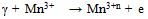
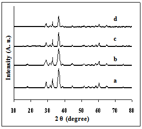
Figure 1. XRD patterns for: a) ZCTAB b) ZTX c) Z d) Zsulph
X-ray diffraction patterns of the investigated manganite samples are presented in Fig. 1. For all samples, the same patterns were observed with well developed (h k l) reflections, which can be well indexed on the basis of the tetragonal spinel structure with the space group of I41/amd JCPDS file (71-2499)[12]. No trace of impurity phases of starting materials is observed in the present patterns, indicating the high purity of the sample.
The spinel lattice of Cu0.1Zn0.9Mn2O4 consists of O2− anions form a close-packed tetragonal lattice in which the Zn2+ and Cu2+ cations are located in tetrahedral sites (labelled as A sites) and Mn3+ are located in octahedral sites (labelled as B sites), respectively; The samples exhibit spinel structure by a formula of Cu0.12+Zn0.92+[Mn3+]2O4. Where the ions inside the square bracket are located in octahedral sites and the ions outside the bracket are in the tetrahedral sites[12].
The X-ray density of all the compositions was calculated using the formula:
(1)
Where Z/ is the number of molecules per unit cell (Z/ = 4); M is the molecular weight; N is the Avogadro’s constant and V is the unit cell of the lattice.
The bulk density (dA) was also measured by the Archimedes principle. The percentage porosity (P) of the samples was then calculated using the relation[13]:
(2)
The values of the bulk density and porosity were both tabulated in Table 1.
Table 1. Density, grain size and porosity of investigated Cu0.1Zn0.9Mn2O4 samples
     
X-ray diffraction line broadening based on (311) peak was used to estimate the crystallites size (DXRD) of the powder by using Scherrer formula[14]:
(3)
Here λ is the wavelength of the Cu Kα radiation (λ = 1.5406 Å), β is the full width half maximum (FWHM) in radians calculated using Gaussian fitting. In our experiment, β was corrected by this formula
(4)
Where βm is the measured FWHM of the sample studied, βS the FWHM of silica, which was used to avoid the broadening from the X-ray instrument. The estimated crystallites sizes of all the samples under investigation are presented in Table 1.
Fig. 2 shows the surface micrographs of the irradiated and unirradiated samples. The SEM-image analysis reveals the role of surfactants as a capping agent. The morphology of the samples prepared in absence of surfactant (Z) showed a range of shapes including deformed polyhedral and spherical shapes. Whereas the sample prepared using triton surfactant (ZTX) showed large grains with spherical shapes. On the other hand, the samples prepared using CTAB surfactant (ZCTAB) showed the formation of nano rods particles. It was reported that CTAB has been successfully used as the morphology-directing agent for the synthesis of one-dimensional nanostructures, such as CuO, PbO2, Pb3O4 and Co3O4 nanorods[15, 16]. In this synthesis, CTAB can be worked as a capping agent or making some the electrostatic interactions; the inorganic precursor and the cationic surfactant can form inorganic–surfactant composite templates. More analysis of SEM-micrographs showed also that the samples prepared using anionic surfactant (Zsulph) exhibit particles with different shapes aggregated with small and large grains sizes. This may be due to some kind of attraction forces between negative surfactant anions and the positive charges molecules of Cu, Zn, and Mn ions leading to agglomerate of particles during the hydrothermal process. Generally, the different morphologies and sizes of crystallites formed during the hydrothermal crystallization in presence of surfactants can be explained on the basis of the balance between nucleation and growth rates. With increase in each of the supersaturation and adsorption of surfactant on the crystal faces, both growth and nucleation rates increase. Consequently, when the growth rate dominates over the nucleation rate, crystallite sizes increase, while in the case of nucleation rate domination, crystallite size decreases[17].
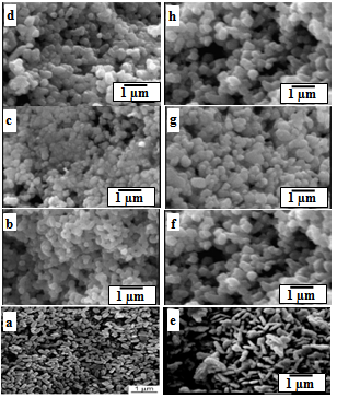
Figure 2. SEM: a) ZCTAB b) ZTX c) Z d) Zsulph e) Z*CTAB f) Z*TX g) Z* h) Z*sulph
SEM micrographs of irradiated samples showed a surface morphology and voids between the particles grains differs to some extent than that of unirradiated ones. And in the same time, the pores sizes became to some extent larger after irradiation process. This refers to that the high ionization radiation creats some defects diffusing in the crystals to produce some effects on the surface of the sample.
The nano rods particles showed in ZCTAB samples have average length of 80 nm and diameter of 40 nm according to TEM image Fig. 3. Generally, the mean particle sizes DTEM of all samples investigated lie between 17 -89 nm, Table (1), which is smaller than DXRD. This may be attributed to either the presence of non-crystalline materials at the lattice surface or to the different approach of two techniques. In XRD, the crystals are randomly distributed; the estimated crystal size from XRD was the average size of the length, and the accuracy of the Scherre`s equation is affected by many factors such as diffraction line width, defects, surface tension , so the Scherrer formula may induce some errors in measuring the absolute values of the crystallite size. The size of voids in irradiated samples is smaller than that of unirradiated ones. This may be attributed to the creation of some defects produced by ionizing radiation.
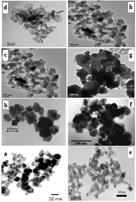
Figure 3. TEM: a) Zsulph b) Z c) ZTX d)ZCTAB e) Z*sulph f ) Z* g) Z*TX h) Z*CTAB

3.2. Electrical Properties

3.2.1. Dc Conductivity
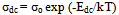
The electrical properties of transition metal oxides with spinel structure depend on several factors, including the method of synthesis, grain size and chemical composition. The dc-conductivity (σdc) of the samples investigated is evaluated using the relation:
(5)
where Rdc is the dc resistance, l is the thickness, and A is the area of the electrode deposited on the sample. The temperature dependence of dc-conductivity for all γ-irradiated and unirradiated samples showed the same behavior, Fig. 4. The figure shows that the electrical conduction in the material is a thermally activated process and it can be explained in accordance with the relation:
(6)
Where σo is the pre-exponential factor, Edc is the activation energy k is the Boltzmann constant. From the slopes of the plots the activation energy values Edc have been calculated and listed in Table 2. It is evident to see that the conductivity increases with increasing the crystallite size. This is due to the fact that samples with small grains contain more number of grain boundaries than grains. The grain boundaries are the regions of mismatch between the energy states of adjacent grains and hence act as barriers to the flow of electrons causing a decrease in conductivity with decreasing particle size.
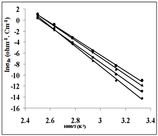
Figure 4. The temperature dependence of DC-conductivity for: (♦), ZSulph; (■), Z; (▲), ZTX; (●), ZCTAB
In other words, it can be said that the variation in electrical properties with the particle size is mainly attributed to the spatial confinement of free and bound charges, and disorder grain boundary. It had been reported that the grain boundaries in nanocrystalline materials exhibit a random atomic arrangement without short or long range order[18]. However, the obtained results refer to that the nature and volume fraction of the grain boundaries are very important in determining the electrical properties of consolidated nanoparticles.
The electrical conductivity values obtained in our Cu0.1Zn0.9Mn2O4 samples are higher than that obtained for nano-ZnMn2O4 (5.3x10⁻⁷ ohm-1 cm-1)[19]. This refers to that the addition of Cu+2 causes a change in the valence states of Mn-ions present in the investigated samples and hence in their conductivity value.
Gamma irradiated process produces an increase in the conductivity values without a change in the activation energies, Table 2. This may be attributed to the following interaction:
(5)
This interaction leads to a change in the arrangement of cations in both tetrahedral and octahedral sites of the spinel lattice. The ionization of Mn3+ to Mn3+n (oxidation states higher than 3+ i.e. Mn4+ or Mn5+…etc.) by irradiation causes a creation of an equivalent proportion of Mn2+ on the same sites, in order to maintain the electrical neutrality. This leads to the formation of Cu2+0.1Zn2+0.9[Mn3+2-2xMn2+x Mn4+x] O42-. The formation of this cation distribution causes an increase in the hopping rate of electrons between the different valence states of Mn-ions and hence an increase in the conductivity. It should be mentioned here that the distances between the ions present on octahedral sites are smaller than that present between the tetrahedral sites, which lead to increase the effective contribution of the octahedral ions in the conduction process.
Table 2. Conductivity data of γ-irradiated and unirradiated Cu0.1Zn0.9Mn2O4 samples at 300 K
     
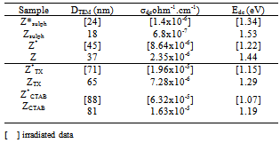
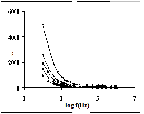
3.2.2. AC-conductivity
In order to give information on the type of polarization present in the samples, the ac-electrical conductivity (σac), at temperatures range of 300-400 K and at frequency range of 102 – 106 Hz were studied. The ac-conductivity σac (ω) was calculated according to
(7)
Where σt (ω) is the measured total frequency-dependent conductivity.
Figure 5. The frequency dependence of AC-conductivity for: (■); Z(Sulph), (♦);Z, (▲); ZTX, (x); ZCTAB(300K), ( ); ZCTAB(340K), (●); ZCTAB(380K), (+); ZCTAB(400K)
Fig. 5 shows the frequency dependence of σac at 300 K for unirradiated samples. The same variation is also observed for irradiated samples with different particle sizes. All the samples show an increasing trend in the ac - conductivity as the frequency increases. However, as the frequency increases the conductivity becomes more and more frequency dependent. The origin of frequency dependence of conductivity in the relaxation phenomenon arises due to mobile charge carriers[20]. In a hopping model, it is possible to distinguish different characteristic regions of frequency. In our case, at low frequencies the conductivity is low due to grain boundary effect which acts as hindrance for mobility of the charge carriers. The hopping mechanism becomes the sole contribution to the conductivity process in the frequency regions where the conductivity is strongly dependent on frequencies.
3.2.3. Dielectric Behavior
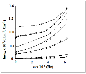
The frequency dependence of dielectric constant ε`and dielectric loss ε`` of nanosized Cu0.1Zn0.9Mn2O4 at different temperatures is studied. A similar trend is observed for all irradiated and unirradiated samples, some typical plots are shown in Fig 6 and Fig. 7. It shows dielectric dispersion where both real and imaginary dielectric constant decreases rapidly with increasing frequency in low-frequency region while it approaches almost frequency independent behaviour in high frequency region. The decrease in imaginary part of dielectric constant is pronounced more in comparison to real dielectric constant. The dielectric dispersion curve can be explained on the basis of Koop's theory[21] based on the Maxwell–Wagner model for the in-homogeneous double structure[22]. According to this model the dielectric structure was supposed to be composed of the double layer. The first layer is of fairly well conducting materials, which is separated by the second thin layer (grain boundaries) of relatively poor conducting substance. The grain boundaries were found to be more effective at lower frequencies while the magnetite grains are more effective at higher frequencies. In present samples, Cu0.1Zn0.9Mn2O4 are dipolar materials due to the presence of majority Mn3+ ions and minority divalent ions in them. The electron exchange between trivalent and divalent ions gives local displacement of electrons in the direction of applied electric field thus inducing polarization in manganite. The decrease in the complex permittivity with increasing frequency is explained to be due to the decrease of polarization of the dipoles when electric field propagates with high frequency. In other words, in dielectric nanostructured samples, interfaces with large volume fractions contain a large number of defects, such as dangling bonds, vacancies, vacancy clusters, and micro porosities, which can cause a change of positive and negative space charge distribution in interfaces. When subjected to an electric field, these space charges move. When they are trapped by defects, a lot of dipole moments are formed. At low frequency region these dipole moments are easy to follow the change of the electric field[23]. So the dielectric loss and hence the dielectric constant shows a large value at low frequency.
For all investigated samples, the dielectric constant ε` was found to increase with increasing the particle size. This can be explained on the basis of many factors, such as amorphousness of surface, high surface energy, micro mechanical stress, surface domain depolarisation, domain wall effects, and so on.
Figure 6. The frequency dependence of dielectric constant of: (●), ZSulph; (▲), Z; (■), ZTX; ( ♦), ZCTAB(300K); ( ), ZCTAB(400K)
Figure 7. The frequency dependence of dielectric loss of : (●), ZSulph; (▲), Z; (■), ZTX; ( ♦), ZCTAB(300K), ( ), ZCTAB(400K).
The results obtained showed also that each of the dielectric constant and the dielectric loss increases with an increase of temperature. This is expected because as the temperature increases, the resistivity of the samples decreases and polarization increases. With the increase in temperature the thermal activation enhances the number of dipoles available for polarization.

3.3. Magnetic Properties

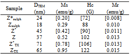
Vibrating sample magnetometer (VSM) was used to investigate the magnetic properties of γ-irradiated and unirradiated Cu0.1Zn0.9Mn2O4 at room temperature. All samples showed narrow hysteresis loops, indicating their slight ferromagnetism. Typical plot is shown in Fig. 8. The irradiated ones showed the same behavior. The saturation magnetizations Ms of the samples were found by extrapolating M vs. 1/H plot to 1/H=0. The variation trend of Ms, Hc and Mr was illustrated in Table 3. From which it can be seen that magnetization (Ms) values for irradiated are higher than unirradiated ones and increase in the following order: ZCTAB > ZTX > Z > Zsulph
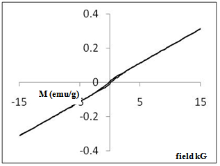
Figure 8. Room temperature magnetic hysteresis loop of Z sample
The ferromagnetic properties of studied samples were attributed to the simultaneous presence of Mn4+ and Mn3+ and Mn2+ ions. They give rise to ferromagnetism via the double-exchange mechanism. Zn and Cu -ions acting as the retardant of the magnetic interaction between the manganese ions. The increase in ferromagnetic character of the samples by irradiation, Table 3, may be attributed to the increase occurring in the ratio of oxidizing and reducing amount of Mn – ions such as Mn3+/ Mn4+ comparable with that present in unirradiated ones, as mentioned above. In summary, the different ferromagnetic properties values of different samples may be attributed to the different Mn3+/Mn4+ compositions.
Table 3. Magnetic Properties parameters of Cu0.1Zn0.9Mn2O4
     
The nanorod sample ZCTAB exhibit saturation magnetization (Ms) value, which is higher than that of other samples. This increase in magnetic properties may be strongly dependent on the growth direction of[110] which is one of the easiest magnetization in the spinel system[24]. Similar results were also found with Fe2O3 nanowires[25].
The increase observed in saturation magnetization with the increase in particle size, Table 3, is attributed to the nature of ultrafine particles, including the surface disorder and surface spin canting due to large surface to volume ratio for nanoparticular system[26, 27]. This may be also attributed to different mechanisms, such as the existence of a magnetically dead layer on the particles surface, the existence of canted spin or the existence of a spin glass like behavior of the surface spins[24-28].

4. Conclusions

Nanocrystalline Cu0.1Zn0.9Mn2O4 were prepared in the range of 18-85 nm using hydrothermal method in presence and absence of surfactants. XRD showed a tetragonal spinel structure for the γ- irradiated and unirradiated samples. The size of the prepared particles has been confirmed through X-ray diffraction and TEM techniques. SEM and TEM images showed surface and particle morphology depends on each of the type of surfactants used and irradiation process. The pores sizes became also smaller after γ-irradiation process. Both ac- and dc-conductivity follows Arrhenius-type thermally activated conduction over temperature range investigated and referring to a semiconducting behavior for the γ-irradiated and unirradiated nano Cu0.1Zn0.Mn2O4 samples. The irradiation process causes an increase in the conductivity values. Hopping mechanism between different oxidation states of Mn-ions in Cu2+0.1 Zn2+0.9[Mn3+ 2-2x Mn2+xMn4+x] O42-samples is used to explain the conducting behavior. The dielectric constant (ε′) and dielectric loss factor (ε′′) decreases exponentially with increasing the measured frequencies and increases with increasing temperature at each individual frequency due to the relaxation of the dipole molecules. All studied samples showed ferromagnetic behavior which increases with increasing each of the particle size and irradiation process. The relation between morphology (nano rod) and magnetic performance is observed.

References

[1]  T. Mousavand, S. Ohara, M. Umetsu, J. Zhang, S. Takami, T. Naka, T. Adschiri, Hydrothermal synthesis and in-situ surface modification of boehmite nanoparticles in supercritical water. J. Supercrit. Fluids 40 (3) (2007)397-404.
[2]  D.G. Shchukin, G.B. Sukhorukov Nanoparticle Synthesis in Engineered Organic Nanoscale Reactors, Adv. Mater. 16 (8) (2004) 671–682.
[3]  J. Oh, J. Lee, S. J. Kim, S.B. Han, K. Park, TiO2 Branched Nanostructure Electrodes Synthesized by Seeding Method for Dye-Sensitized Solar Cells, Chem.Mater., 22 (3)(2010) 1114–1118.
[4]  T. Nomura, T. Mori, H. Arima, Y. Konishi, Shape and size control of barium chromate nanoparticles using reverse micelle, Adv. Powder Technol., 20 ( 1) (2009)101-105.
[5]  Y. Li, Y. Guo, R. Tan, P. Cui, Y. Li, W. Song, Synthesis of SnO2 nano-sheets by a template-free hydrothermal method, Mater. Lett., (63)( 24-25) (2009) 2085-2088.
[6]  X. Shi, Y. Xiao, L. Yuan, J. Sun, Hydrothermal synthesis and characterizations of 2D and 3D 4ZnO·B2O3·H2O nano/microstructures with different morphologies, Powd. Technol., 189(3) (2009) 462-465
[7]  S. Kurien, J. Mathew, S. Sebastian, S.N. Potty, K.C. George, Dielectric behavior and ac electrical conductivity of nanocrystalline nickel aluminate Mater. Chem. Phys., 98 (2-3) (2006) 470-476.
[8]  T. Tuner, M. Korkmaz, ESR study of ascorbic acid irradiated with gamma- rays, J. Radioanaly. Nucl. Chem. 273 (2007) 609-614.
[9]  S. Guillemet-Fritsch, C. Chanel, J. Sarrias, S. Bayonne, A. Rousset, X. Alcobe, M. L. Martinez Sarriòn, Structure, thermal stability and electrical properties of zinc manganites, Solid State Ionics, 128 (1-4) (2000) 233-242.
[10]  G. Ferraris, G. Fierro, M. Lo Jacono, M. Inversi, R. Dragone, A study of the catalytic activity of cobalt–zinc manganites for the reduction of NO by hydrocarbons, Appl. Catal. B 36 ( 4) ( 2002) 251-260.
[11]  F. Liu, R. Kirchheim, Nano-scale grain growth inhibited by reducing grain boundary energy through solute segregation, J. Cryst. Growth, 264( 1-3) (2004) 385-391.
[12]  A.C.F.M. Costa, A.M.D. Leite, H.S. Ferreira, R.H.G.A. Kiminami, S. Cava, L. Gama, Brown pigment of the nanopowder spinel ferrite prepared by combustion reaction, J. Eur. Ceram. Soc. 28 (2008) 2033–2037.
[13]  A. Karamanov, M. Pelino, Induced crystallization porosity and properties of sintereds diopside and wollastonite glass-ceramic, J. Eur. Ceram. Soc., 28 (3) ( 2008) 555-562.
[14]  H.P. Klug, L.E. Alexander, X-ray diffraction procedures for polycrystalline and amorphous materials, Wiley, New York (1970).
[15]  S. Lian, E. Wang, Lei Gao, Lin Xu, Fabrication of single-crystalline Co3O4 nanorods via a low-temperature solvothermal process, Mater. Lett., 61 (18) (2007) 3893-3896.
[16]  M. Cao, C. Hu, Y. Wang, Y. Guo, C. Guo and E.B. Wang, Chem. Commun. 1884 (2003).
[17]  L. Carbone, P. D. Cozzoli, Colloidal heterostructured nanocrystals: Synthesis and growth mechanisms, Nano Today, 5 (5) (2010) 449-493.
[18]  V. Biju, M. Abdul Khadar, Analysis of AC electrical properties of nanocrystalline nickel oxide, Mater. Sci. . Eng.: A 304–306 (2001) 814–817.
[19]  M. Khairy, M. A. Mousa, Synthesis, characterization, catalytic and electrical conductivity of nanosized gamma irradiated and unirradiated ZnMn2O4, in press.
[20]  B. Treev, “Physics of dielectric materials”, 1988, Mir. Moscow.
[21]  C.G. Koops, On the Dispersion of Resistivity and Dielectric Constant of Some Semiconductors at Audio frequencies, Phys. Rev., 83 (1951) 121 -124.
[22]  T. Hanai and K. Sekine Theory of dielectric relaxations due to the interfacial polarization for two-component suspensions of spheres, Colloid & polymer Sci.64 (1986) 888-895 .
[23]  N W Grimes, Dielectric constants and the oxide additivity rule-comments on a recentinvestigation of MgAl2O4 spinel, J. Phys.: Condens. Matter 4 (1992 ) L567.
[24]  Z. Jiang, J. Han and X. Liu, Study on Structure and Magnetization of Spinel Ferrites, Adv. Mater. Res. (152 - 153) (2010) 274-278.
[25]  R.K. Gupta, K. Ghosh, L. Dong, P.K. Kahol, Structural and magnetic properties of phase controlled iron oxide rods, Mater. Lett., 65(2)(2011)225-228.
[26]  A. Ceylan, S. Ozcan, C. Ni, S. I. Shah, Solid state reaction synthesis of NiFe2O4 nanoparticles, J. Magn. Magn. Mater. 320 (2008) 857-863.
[27]  R.H. Kodama, Magnetic nanoparticles - Condens. Matter, J. Magn. Magn. Mater., 200, (1-3)(1999)359-372.
[28]  J. Chandradass, M. Balasubramanian, Ki Hyeon Kim, Size effect on the magnetic property of CoAl2O4 nanopowders prepared byreverse micelle processing, J. Alloys Compd. 506 (2010) 395–399.