-
Paper Information
- Next Paper
- Previous Paper
- Paper Submission
-
Journal Information
- About This Journal
- Editorial Board
- Current Issue
- Archive
- Author Guidelines
- Contact Us
International Journal of Materials and Chemistry
p-ISSN: 2166-5346 e-ISSN: 2166-5354
2012; 2(4): 173-177
doi: 10.5923/j.ijmc.20120204.10
Properties of Amorphous SnO2 Thin Films, Prepared by Thermal Evaporation
 Abstract
 Reference
 Full-Text PDF
 Full-Text HTML
Shadia J. Ikhmayies
Al Isra University, Faculty of Information Technology, Department of Basic Sciences-Physics, Amman, 16197, Jordan
Correspondence to: Shadia J. Ikhmayies , Al Isra University, Faculty of Information Technology, Department of Basic Sciences-Physics, Amman, 16197, Jordan.
| Email: |  |
Copyright © 2012 Scientific & Academic Publishing. All Rights Reserved.
Tin oxide (SnO2) thin films of thickness in the range 100-600 nm are prepared on glass substrates by thermal evaporation at ambient temperatures. The films are characterized by recording their transmittance measurements, X-ray diffraction (XRD) patterns, scanning electron microscope (SEM) images and energy dispersion X-ray analysis (EDAX). It is found that the films have high transmittance and non-sharp absorption edge. XRD diffractograms showed that the films are amorphous and the SEM micrographs depicted that the surfaces are smooth, uniform and well covered with the material. The EDAX analysis showed that the films are deficient in oxygen. Indirect optical bandgap energy is determined and Urbach tailing in the bandgap is observed and the width of the tail which is related with disorder and localized states is estimated.
Keywords: Transparent Conducting Oxides (TCOS), Amorphous Tin Oxide Thin Films, Optical Properties, Urbach Tail, Gas Sensors
Cite this paper: Shadia J. Ikhmayies , "Properties of Amorphous SnO2 Thin Films, Prepared by Thermal Evaporation", International Journal of Materials and Chemistry, Vol. 2 No. 4, 2012, pp. 173-177. doi: 10.5923/j.ijmc.20120204.10.
Article Outline
1. Introduction
- SnO2 is an n-type wide bandgap semiconducting material with direct bandgap energy of 4 eV and indirect bandgap of 2.6 eV[1], where inherent oxygen vacancies act as an n-type dopant[2]. Tin oxide thin films have been used for transparent electrodes in photoelectric conversion devices namely amorphous silicon solar cells, liquid crystal display, gas discharge display, etc.[3]. Perfectly amorphous thin SnO2 films show good electrical response to reducing gases in air and could hence be applied to construct semiconductor gas sensors where the metal oxide films function as a monograin-eqivalent active layer[4]. Amorphous SnO2 can also be used in extended gate field-effect transistors (EGFET) as pH sensor, where the sensitive part is made of SnO2/Al structure. This device can be used to detect and to quantify any kind of substances that can produce or consume protons like an enzymatic reaction, therefore showing a large range of applications as biosensors[5]. There are different methods to prepare SnO2 films such as, atomic layer deposition (ALD)[6], reactive magnetron sputtering[7], chemical vapor deposition ([8],[9]), dip coating[10], spray pyrolysis (SP) ([3],[11-14]), and evaporation[8]. Thermal evaporation method was choose to produce SnO2 thin films in this work because the deposition by this technique does not present any compositional problems, beside the fact that it is a low temperature producing amorphous films. To increase this probability the technique, which increases the probability of films were deposited at ambient temperature.In this work the properties of amorphous SnO2 thin films are investigated by studying their structure, morphology, composition and transmittance at room temperature. The films were characterized by X-ray diffraction (XRD), scanning electron microscope observations, energy dispersive analysis by X-ray (EDAX), and transmittance measurements. The indirect bandgap of the films and Urbach tailing were estimated and discussed.
2. Experimental Part
- Undoped SnO2 thin films are deposited by thermal evaporation at ambient temperature on glass substrates of dimensions (6×2.6×0.1cm3) in a high vacuum system (~10-5 mbar) provided with a Turboe pump. The substrates are cleaned in methanol, followed by distilled water. The evaporation rate is about 10 Å/s and it is measured by a cooled quartz crystal monitor. The distance between the source and the substrate is about 30 cm. Films of thickness 50-600 nm are produced through different individual evaporations. The films showed light brown colour that becomes darker with film thickness.The transmittance of the films is measured by using a double beam Shimadzu UV 1601 (PC) spectrophotometer with respect to a piece of glass similar to the substrates in the wavelength range 300-1100 nm. The thickness of the films is estimated from the interference maxima and minima in the transmittance by using the method of Alvin[15]. X-ray measurements are made with a Philips PW1840 Compact X-ray diffractometer system with Cu Kα (λ = 1.5405 Å). The SEM images are taken by a FEI scanning electron microscope (Inspect F 50), which is supplied by energy dispersive analysis by X-rays (EDAX), so the compositional analysis of the films is performed by the same system.
3. Results and Discussion
- Fig.1 displays the X-ray diffractograms for two SnO2 thin films of different thickness 200 and 600 nm, deposited on glass substrates at ambient temperature. Both diffractograms showed a broad hump including the positions of the (1 1 0) and (1 0 1) lines, indicating that the films have amorphous structure. It is noticed that the peak of the hump for the thicker film is centred at about 2θ = 29°, while that of the thinner one is centred at about 2θ = 28°. Beside this the width of the hump of the thinner film is larger than that of the thicker one, and hence the full widths at half maximum FWHM are 4.5 and 5.0° for the thicker and thinner films respectively. From these results we conclude that the thicker film is closer to the transformation from the amorphous phase to the polycrystalline phase than the thinner one.
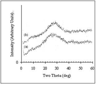 | Figure 1. X-ray diffractograms of two thermally evaporated SnO2 thin films with thickness a) 200 nm. b) 600 nm |
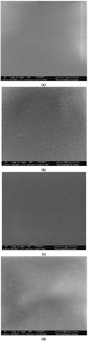 | Figure 2. SEM micrographs at two magnifications of two thermally evaporated SnO2 thin films of thickness 300 nm (a) and (b); and 400 nm (c) and (d) |
 | (1) |
 is the absorption coefficient,
  is Planck's constant,
  is the frequency of the radiation,
  is the characteristic parameter (independent of photon's energy) for respective transitions,
  denotes photon's energy,
  is the optical energy gap and
  is the number which characterizes the transition process, where
  for most amorphous semiconductors (indirect transition) and
  for most of crystalline semiconductors (direct transition).
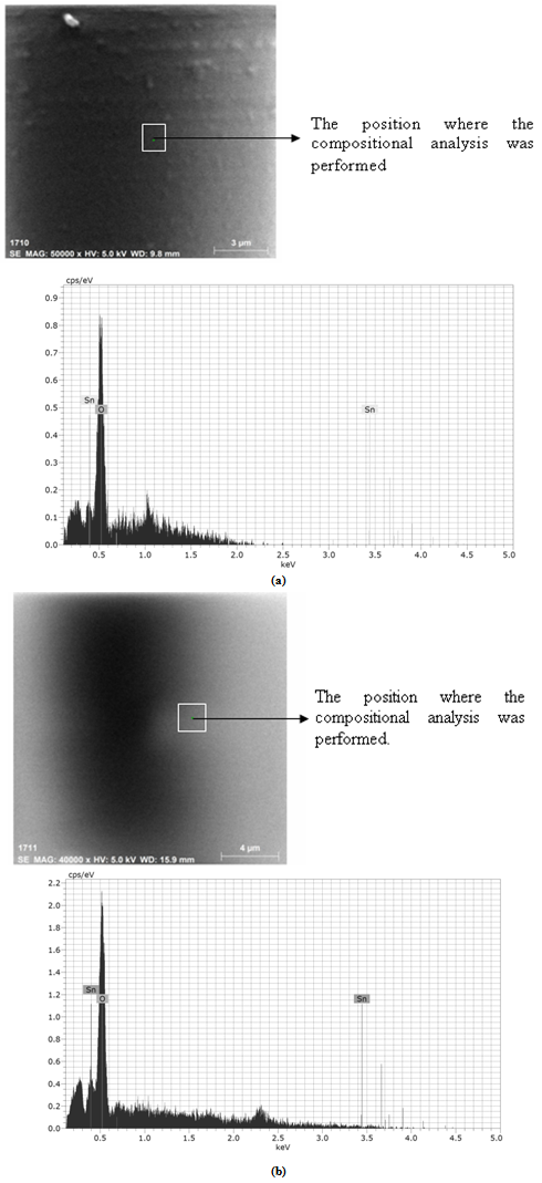 | Figure 3. EDAX patterns for amorphous SnO2 thin films and accompanied SEM images to show the point at which the compositional analysis is performed. a) Film thickness = 300 nm. b) Film thickness = 400 nm |
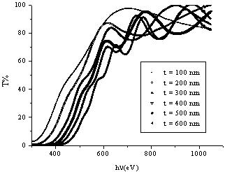 | Figure 4. Transmittance of thermally evaporated SnO2 thin films of different thickness against photon's energy |
 against the photon's energy. A linear fit was performed for each curve and the indirect optical bandgap energy Ein was estimated from the intercept with the energy axis with neglecting phonon's energy. The deduced values are inserted in table 2. As the table shows, the indirect optical bandgap energy Ein decreases with film thickness. These values are close to the values that we obtained in a previous work[17] for partially polycrystalline SnO2 thin films prepared by thermal evaporation. On the other hand, these values are smaller than the values given in our previous work[11] for polycrystalline SnO2:F thin films prepared by the spray pyrolysis technique, the values obtained by Díaz-Flores et. al.[1], the values given by Mohammad and Abdul-Ghafor[18], and those given by Mohammad[19] for spray-deposited SnO2:F thin films. The reason of this difference is that the optical bandgap increases with doping and our films in this work are not doped.
 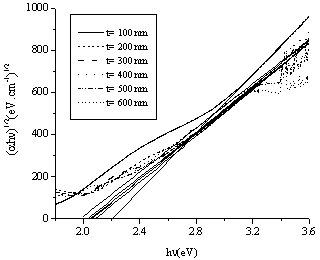 | Figure 5. The plot of  against the photon's energy against the photon's energy  with the linear fits for amorphous, thermally evaporated SnO2 thin films of different thickness with the linear fits for amorphous, thermally evaporated SnO2 thin films of different thickness |
 | (2) |
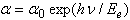
 is a constant and
  is the width of the Urbach tail. The exponential tail appears because disordered and amorphous materials produce localized states extended in the bandgap. The absorption edge of these materials at α less than 104 cm-1, empirically follows the Urbach law, and this is interpreted as evidence for the existence of localized states. But Urbach law can be applicable to α larger than 104 cm-1[20]. To find the width of Urbach tail
  a plot of
  against the photon's energy is shown in Fig.6. Linear fits were performed and the values of
  and
and  for the whole set of curves were estimated and inserted in table 2.
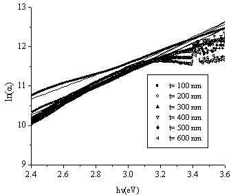 | Figure 6. The plot of  against the photon's energy against the photon's energy  with the linear fits for amorphous, thermally evaporated SnO2 thin films of different thickness with the linear fits for amorphous, thermally evaporated SnO2 thin films of different thickness |
|
4. Conclusions
- Amorphous SnO2 thin films of thickness in the range 100-600 nm were prepared by thermal evaporation at ambient temperature. X-ray diffractograms showed a wide hump which confirms the amorphous structure of the films. SEM micrographs showed smooth surfaces without features in agreement with the amorphous structures observed by XRD patterns. EDAX analysis revealed that the films are deficient in oxygen which means that they are n-type. The transmittance of the films is very high in the visible and infrared regions. The indirect bandgap and Urbach tail were estimated and related to film thickness. The deduced values are compared with those obtained by different authors.
ACKNOWLEDGEMENTS
- I would like to thank Sameer Farrash from the physics department in the University of Jordan for producing the films by thermal evaporation. Also I want to thank Waddah Fares Mahmoud and Azzam Karadsheh from the department of geology in the University of Jordan for taking the SEM micrographs with EDAX analysis and for recording XRD diffractograms, respectively.
References
| [1] | L. L. Díaz-Flores, R. Ramírez-Bon, A. Mendoza-Galván, E. Prokhorov, J. González-Hernández, " Impedance spectroscopy studies on SnO2 films prepared by the sol–gel process", Elsevier, J. Phys. Chem. Solids, Vol.64, pp.1037-1042, 2003. |
| [2] | Z. Chen, J. K. L. Lai, C. H. Shek, H. Chen, "Synthesis and structural characterization of rutile SnO2 nanocrystals", Cambridge University Press, J. Mater. Res., Vol.18, no.6, pp. 1289-1292, 2003. |
| [3] | S.M. Rozati, " The effect of substrate temperature on the structure of tin oxide thin films obtained by spray pyrolysis method, Elsevier, Mate. Charact., Vol.57, pp.150-153, 2006. |
| [4] | J. Sundqvist, "Employing Metal Iodides and Oxygen in ALD and CVD of Functional Metal Oxides", Acta Universitatis Upsaliensis, Uppsala, Ch.4, 35-56, 2003. |
| [5] | P. D. Batista, M. Mulato, C. F. de O. Graeff, F. J. R. Fernandez, F. Das C. Marques, "SnO2 Extended Gate Field-Effect Transistor as pH Sensor", Sociedade Brasileira de Fisica, Braz. J. Phys. Vol.36, no. 2A, pp. 478-481, 2006. |
| [6] | J. W. Elam, D. A. Baker, A. J. Hryn, A. B. F. Martinson., M. J. Pellin, J. T. Hupp, " Atomic layer deposition of tin oxide films using tetrakis (dimethylamino) tin", AVS, J. Vac. Sci. Technol. A, Vol.26, no.2, pp.244-252, 2008. |
| [7] | A. S. Ryzhikov, R. B. Vasiliev, M. N. Rumyantseva, L. I. Ryabova, G. A. Dosovitsky, A. M. Gilmutdinov, V. F. Kozlovsky, A. M. Gaskov, "Microstructure and electrophysical properties of SnO2, ZnO and In2O3 nanocrystalline films prepared by reactive magnetron sputtering", Elsevier, Mat. Sci. Eng. B-Solid., Vol.96, pp.268-274, 2002. |
| [8] | P. Montmeat, "Thin film membranes for the improvement of gas sensor selectivity", Doctorate thesis. École Nationale Supérieure des Mines de Saint-Étienne (ENSMSE): a graduate school for science and technology, France, 1999. |
| [9] | J. Sundqvist and A. Hårsta, "Growth of SnO2 thin films by ALD and CVD: A comparative study", in Proceedings of the sixteenth Int. CVD Conf., Paris, France, 1, pp.511, 2003. |
| [10] | V. Geraldo, L. V. de Andrade Scalvi, E. A. de Morais, C. V. Santilli, S. H. Pulcinelli, "Sb Doping effect and oxygen adsorption in SnO2 thin films deposited via sol-gel.", ABM, ABC, ABPol, Mat. Res.,Vol.6, no.4, pp.451-456, 2003. |
| [11] | S. J. Ikhmayies, R. N. Ahmad-Bitar, "An investigation of the bandgap and Urbach tail of spray-deposited SnO2:F fhin films", IOP, Phys. Scripta., Vol.84, pp.055801, 2011. |
| [12] | S. J. Ikhmayies, R. N. Ahmad-Bitar, "Effect of the substrate temperature on the electrical and structural properties of spray-deposited SnO2:F thin films", Elsevier, Mat. Sci. Semicon. Proc., Vol.12, no.3, pp.122-125, 2009. |
| [13] | S. J. Ikhmayies, R. N. Ahmad-Bitar, "The effects of post-treatments on the photovoltaic properties of spray-deposited SnO2:F thin films", Elsevier, Appl. Surf. Sci., Vol.255, pp.2627-2631, 2008. |
| [14] | S. J. Ikhmayies, R. N. Ahmad-Bitar, " Effect of Processing on the Electrical Properties of Spray-Deposited SnO2:F Thin Films, Science Publications, Am. J. Applied Sci., Vol.5, no.6, pp.672-677, 2008. |
| [15] | G. M. Alvin, " Optical interference method for the approximate determination of refractive index and thickness of a transparent layer", Optical Society of America, Appl. Optics, Vol.17, no.17, pp.2779-2787, 1978. |
| [16] | E. R. Shaaban, N. Afify, A. El-Taher, "Effect of film thickness on microstructure parameters and optical constants of CdTe thin films", Elsevier, J. Alloy. Compd., Vol.482, pp.400-404, 2009. |
| [17] | S. J. Ikhmayies, R. N. Ahmad-Bitar, "An investigation of the bandgap and Urbach tail of vacuum-evaporated SnO2 thin films", Elsevier, Renew. Energ.,doi:10.1016/j.renene.2012.01.045., 2012. |
| [18] | M. T. Mohammad, W. A. Abdul-Ghafor, "Properties of fluorine-doped SnO2 films prepared by the spray pyrolysis Technique", Wiley-VCH, Phys. Stat. Sol. (A), Vol.106, pp.479-483, 1988. |
| [19] | M. T. Mohammad, "Performance and characteristics of Al-PbS/SnO2:F selective coating system for photothermal energy conversion", Elsevier, Sol. Energ. Mat. Sol. C. Vol.20, no.4, pp.297-305, 1990. |
| [20] | Y. Natsume, H. Sakata, T. Hirayama, "Low temperature electrical conductivity and optical absorption edge of ZnO films prepared by chemical vapor deposition", Wiley-VCH, Phys. Stat. Sol. (A), Vol.148, pp.485-495, 1995. |
| [21] | J. Melsheimer, D. Ziegler, "Band gap energy and Urbach tail studies of amorphous, partially crystalline and polycrystalline tin dioxide", Elsevier, Thin Solid Films., Vol.129, pp.35-47, 1985. |