-
Paper Information
- Next Paper
- Previous Paper
- Paper Submission
-
Journal Information
- About This Journal
- Editorial Board
- Current Issue
- Archive
- Author Guidelines
- Contact Us
International Journal of Materials and Chemistry
p-ISSN: 2166-5346 e-ISSN: 2166-5354
2012; 2(4): 165-172
doi: 10.5923/j.ijmc.20120204.09
Structural, Optical and Electrical Properties of Nanostructured CdS:CuS Composite Thin Films Grown by CBD Method
 Abstract
 Reference
 Full-Text PDF
 Full-Text HTML
A. U. Ubale , K. S. Chipade , M.V. Bhute , P. P. Raut , G. P. Malpe , Y. S. Sakhare , M. R. Belkhedkar
Nanostructured Thin film Materials Laboratory, Departments of Physics, Govt. Vidarbha Institute Sciencesand Humanities, Amravati , 444604, Maharashtra, India
Correspondence to: A. U. Ubale , Nanostructured Thin film Materials Laboratory, Departments of Physics, Govt. Vidarbha Institute Sciencesand Humanities, Amravati , 444604, Maharashtra, India.
| Email: |  |
Copyright © 2012 Scientific & Academic Publishing. All Rights Reserved.
Synthesis of nanostructured composite chalcogenide materials have been the subject of much interest in basic research because of their photovoltaic applications. The ternary composite semiconducting thin films of CdS:CuS were successfully deposited onto glass substrates at room temperature by Chemical Bath Deposition (CBD) method using cadmium acetate, cupric acetate and sodium thiosulphate in acidic medium. The films were characterized by using X-ray diffraction, scanning electron microscopy, Fourier transform infrared (FTIR) spectrum, optical absorbance, dc electrical resistivity measurements and thermo-emf techniques.Theas deposited CdS:CuS composite thin films are polycrystalline in nature with hexagonal phase of CdS and CuS with average crystallite size of 23 nm.The optical band gap and activation energy of CdS:CuS thin film is found to be 2.77 and 0.03 eV respectively. The electrical resistivity at 373 K temperature was found to be of the order of 6.87 Ω-cm and it decreases as temperature increases indicating its semiconducting nature.The thermo-emf measurement conforms p-type conductivity of CdS:CuS.The water angle contact measurement conforms hydrophilicnature of CdS:CuS thin films.
Keywords: Cds:Cus Thin Films, CBD Method, Chalcogenide, Optical, Electrical Properties
Cite this paper: A. U. Ubale , K. S. Chipade , M.V. Bhute , P. P. Raut , G. P. Malpe , Y. S. Sakhare , M. R. Belkhedkar , "Structural, Optical and Electrical Properties of Nanostructured CdS:CuS Composite Thin Films Grown by CBD Method", International Journal of Materials and Chemistry, Vol. 2 No. 4, 2012, pp. 165-172. doi: 10.5923/j.ijmc.20120204.09.
Article Outline
1. Introduction
- In recent years, the development of nanostructured materials in the form of thin films occupy a prominent place in basic research and solid state technology due to their expanding range of potential applications in the diverse field such as photovoltaic cells, electronic components, fabrication of large area photodiode arrays,photoconductors, sensors, antireflection coatings, optical filters, surface acoustic wave devices, solar selective coatings and solar cells etc.[1]. The nanostructured material has high surface area to volume ratio and hence shows different structural, optical, electrical, magnetic and dielectric properties than bulk. A nanostructured thin films material layer can be grown on a substrate by controlled condensation of the individual atomic, molecular or ionic species either directly by a physical process or through a chemical and/or electrochemical reaction. The application of nanostructuredthin films can be utilized to enhance the efficiency of semiconductor or photovoltaic devices as well as to lower their effective cost. In this regard many nano-structuredma-terials are now being investigated for their potential applications in photovoltaics[2].Cadmium sulphide(CdS) and copper sulphide(CuS) thin films have received great importance since the historic discovery of the photovoltaic properties of CuS thin films in contact with CdS thin films[3]. It is well known that the electrical and optical properties of CdS and CuS thin films play potential role in photoconductors, photovoltaic devices, solar selective coatings, IR detectors etc. Several techniques have been investigated to prepare CdS and CuS thin films. Lokhande[4] have deposited CdS thin films by chemical bath deposition method using sodium thiosulphate as asulphar source in acidic medium. The optical band gap and electrical resistivity of the as-deposited thin films is of the order of 2.55 eV and 103-104 Ω-cm respectively. Mahdi et al.[5] have prepared adhesive homogenous CdS nanocrystalline thin films using microwave assisted chemical bath deposition method onto glass substrate at 80℃ and studied their structural and optical properties. Jaber et al.[6] have deposited CdS thin films by chemical bath deposition technique using ethanolamine as acomplexing agent instead of commonly used ammonia to avoid toxicity and volatility during film preparation. The optical transmittance characterization in UV-Visible range shows that the prepared films have a high transparency ranging from 60 to 80% for photons having wavelength greater than 600 nm. Jatar et al[7] have prepared Al doped CdS thin films by vacuum evaporation technique and discussed their utility in liquid crystal display. Ashour[8] have prepared cadmium sulphide(CdS) thin films by chemical spray pyrolysis technique by varying the substrate temperature in the range of 200-400℃ and reported their physical properties. Lokhande and Pawar[9, 10] have deposited aluminium doped and un-doped CdS films on stainless steel substrate by chemical bath deposition technique and studied their electrochemical properties. Lokhande et al.[11] have deposited copper doped and undopedCdS films on stainless steel strips by chemical bath deposition. Ubale et al.[12] have prepared CuxS thin films by chemical route at room temperature and reported their size dependent physical properties. Nair et al.[13] have reported the optoelectronic and solar properties of chemically deposited CuxS thin films. Fatas et al.[14] have deposited CuxS thin films in alkaline medium by chemical method using CuSO4and thiourea as cationic and anionic source. The optical band-gap is 2.58 eV and electrical resistivity is of the order of 3 x 10⁻³ Ω-cm. Lindroos et al.[15] have prepared polycrystalline copper sulphide thin films by successive ionic layer adsorption and reaction method at room temperature.Now a day’s nanostructured thin films had been studied with the expectation that the new enhanced properties exhibited by various composite materials were useful in various semiconductor devices especially in photovoltaic cells. Although number of reports were available on chemically deposited ternary composite thin films such as HgS–Bi2S3[16], (NiS)x(CdS)1-x[17],(CdS)x(PbS)1−x[18], PbS–CuxS[19], Bi2S3–CuxS[20, 21], Cd1−xZnxS[22–25], Cd1−xFexS[26], (CdS)x(Bi2S3)1−x[27], and reported their potential applications in the range of areas including solar control coating, energy conversion and solar energy utilization, still there is a wide spread interest owing to the variation in structural, electrical and optical properties of nanostructured semiconductor thin films due to their novelty; their properties are different and superior than conventional polycrystalline materials which are very important for semiconductor application. Literature survey reveals that many reports are available on CdS and CuS thin films prepared by CBD method. The present paper deals with the synthesis of nanocrystalline CdS:CuS composite thin films at room temperature by CBD method.Among the various deposition techniques chemical bath deposition (CBD) techniques has attracted much attention of research community as it is a simple and cost effective for deposition of homogeneous and high-quality nanostructured thin films at room temperature. It does not require any sophisticated instrument like vacuum system. The films deposited by this method are uniform and continuous as the solution remains in contact with substrate throughout the process. The various preparative parameters such as pH, ionic concentration, deposition time etc. can be easily controlled to get good quality thin films. The growth of thin film strongly depends on the growth conditions, such as duration of deposition, composition and temperature of solution and topographical and chemical nature of the substrate.The preparative parameters such as ionic concentration of Cd, Cu and sulphar, temperature and pH were optimized to get good quality thin films on glass substrate. The composition dependent structural, morphological, optical and electrical properties of CdS:CuSthin films were studied by X-ray diffraction, scanning electron microscopy, optical absorbance and electrical resistivity measurements.
2. Experimental
- Chemical bath deposition is a simple and attractive method for the fabrication of nanostructuredmetal chalcogenide thin films which is also known as solution growth, controlled precipitation, or simply chemical deposition. The reaction takes place between the dissolved precursors generally in aqueous solution at low temperature. The sulphide precursors such as thiourea, thioactetamide, thiosulphate and sodium sulphide are generally used. In CBD method substrate cleaning is very important as it is one of the factors determining the composition and grain size of the film. There are various cleaning methods depending on the nature of the substrate, type of contaminants and the extent of cleanliness required for thin film deposition. The surface of the substrate will be usually contaminated with fingerprints, oil, lint and dust. In present investigation, the amorphous glass substrates of approximately 100% transmission and size (75 mm x 25 mm × 1.35 mm) supplied by polar industrial corporation (blue star), Mumbai were utilized for deposition purpose.The glass substrates were boiled in the chromic acid for 30 minutes and kept in it for next 48 hours. The slides were then dipped in labolene detergent and washed with double distilled water. Finally the slides were cleaned with ultrasonic cleaner for 10 minutes, dipped in AR grade acetone and dried for 15 min, prior to the deposition.For deposition of CdS:CuS composite thin films by chemical bath deposition, an aqueous solution of cadmium acetate, cupric acetate and sodium thiosulphate were used in acidic medium.For this, 20 ml (0.1M) cadmium acetate (CH3COO)2Cd.2H2O), 20 ml (0.1M) cupric acetate (C3H6CuO4·H2O) and 40 ml (0.1M) sodium thiosulphate (Na2S2O3.5H2O) were mixed in 100 ml beaker at room temperature. Then the concentrated HCL was added drop wise in the reaction mixture to adjust pH to 3.The prepared solution was stirred continuously for 5 minutes to obtain a homogenous solution. The cleaned glass substrates were then immersed into the resultant solution and suspended vertically with the help of specially designed holder. The colour of solution was changed after about 60 min, which indicates initiation of the chemical reaction.The substrate covered with an orange-yellow deposit, were taken out from the bath after 12 hours deposition time, rinsed with distilled water and allowed to dry in air.The thickness of the composite CdS:CuS thin film was measured byweight difference methodusing the relation,
 | (1) |
3. Results and Discussion
3.1. Reaction Mechanism
- The reaction mechanism for deposition of the metal sulphide films from an acidic bath using Na2S2O3 as a sulphar sourcehas previously been reported[28-30]. The deposition of (CdS:CuS) composite thin film is based on the slow release of Cd2+, Cu2+ and S2− ions in the solution, which are then condensed onto the glass substrates. Cadmium acetate (CH3COO)2Cd.2H2O) and cupric acetate (C3H6 CuO4·H2O) were used as sources for Cd2+and Cu2+ ions. The reaction mechanism for the deposition of composite CdS:CuS thin film is proposed as follows,In aqueous solution, Na2S2O3 dissociated as,
 | (2) |
 | (3) |
 | (4) |
 | (5) |
 | (6) |
3.2.Structural Properties
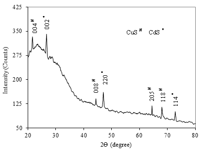
- The structural identification of CdS:CuS composite thin film was carried out from the analysis of the X-ray diffraction pattern taken in the range of 2θ between 20o and 80o. Figure 1 shows the X-ray diffraction pattern of CdS:CuS composite film deposited on glasssubstrate.The diffraction pattern of CdS:CuS composite thin film shows polycrystalline nature with mixed hexagonal lattice due to CdS and CuS. The observed 2θ and d values are in good agreement with standard 2θ and d values due to CdS:CuS. The (002),(220) and (114) orientation corresponds to hexagonal phase of CdS, however the (004),(008),(205) and (118) orientation is due to hexagonal CuS. The CdS peak (002) observed at an angle 26.6790 and CuS peak (220) observed at an angle 47.0500 has more intensity as compared to other orientations. The hexagonal lattice observed for CdS with (002) orientation is in good agreement with earlier reports[31, 32, 33].
 | Figure 1. XRD pattern of CdS:CuS composite thin film |
 | (7) |
3.3. SEM Studies
- Scanning electron microscopy is a convenient method to study the surface morphology of thin films. Surface morphology of material plays an important role in solar energy conversion efficiency of the device. The SEM micrographs of as-deposited CdS:CuS composite thin film (thickness ~ 262 nm) on glass substrate at X100,000 and X50,000 magnification is shown in figure 2. TheCdS:CuS thin film has dense, homogeneous and porous growth morphology.The nanosized grains are uniformly distributed throughout the surface. The grains are quite small with unequal size and shape, also their boundaries are not well defined, and hence it was difficult to calculate the exact average value of grain size from SEM image. The film surface shows spherical flower-like hierarchical morphology with overgrowth. Such Flower like morphology was represented by Lihua Wang et al.[34] for chemically deposited CuS thin films. Also, Figure 2(B) shows growth of nanoleafts on spherical grain; that increases the surface to volume ratio of deposited CdS:CuS material, which can be potential utilized in many optoelectronic and photovoltaic devices.
 | Figure 2. SEM images of CdS:CuS composite thin film on glass substrate at magnification: (a) X100,000, (b) X50,000 |
3.4. Fourier Transforms Infrared Analysis
- Fourier Transform-Infrared Spectroscopy (FTIR) is an analytical technique used to identify organic as well as inorganic materials. This technique measures the absorption of infrared radiation by the sample material versus wavelength.The FTIR spectrum of CdS:CuS composite thin film is as shown in Figure 3.FTIR measurements have been made in the wave number range 400 cm-1 to 4000 cm-1.
 | Figure 3. FTIR spectra of composite CdS:CuSthin film |
3.5. Optical Properties
- The study of optical properties of thin films has special significance in the world of science, technology and industry for the development of new optical devices. Optical absorption study of materials provides useful information to analyze some features concerning the band structure of materials. The optical band gap energy of the semiconductor is an important parameter that plays a major role in the construction of photovoltaic cells. In present report optical properties of the nano-composite CdS:CuS film deposited on glass substrate was studied from the absorption spectra measured by a UV–Visspectrophotometer lambda 25 in the wavelength range 300 to 1100 nm by subtracting the absorption of the glass substrate, which was taken as a reference. The variation of absorbance (αt) with wavelength (nm) for CdS:CuS thin film is shown in figure 4. The sharp absorption edge observed confirms the good optical band edge property of the CdS:CuS thin film. The fundamental absorption, which corresponds to electron excitation from the valance band to conduction band, can be used to determine the nature and value of the optical band gap.
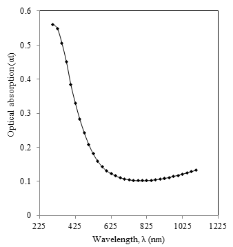 | Figure 4. Variation of optical absorption versus wavelength for CdS:CuS thin film |
 | (8) |
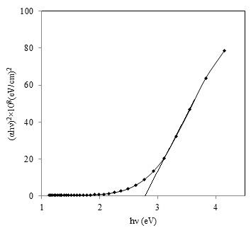 | Figure 5. Plot of (αhν)2 versus hν for as-deposited CdS:CuS thin film |
3.6. Electrical Properties
- The current–voltage (I–V) characteristics of the as-deposited thin film was studied in dark to check nature of contact of CdS:CuS with silver using two-probe method. The typical IV characteristics for CdS:CuS thin films is shown in figure 6.
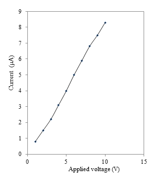 | Figure 6. Variation of current (µA) with applied voltage (V) for CdS:CuS composite thin film |
 | (9) |
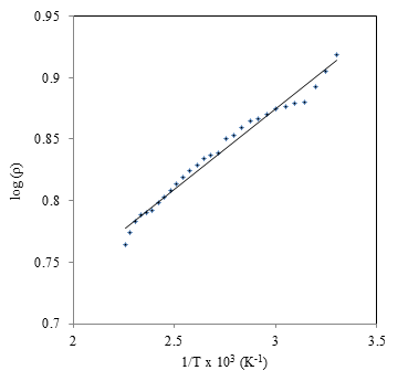 | Figure 7. Variation of Log of resistivity with 1/T for as deposited CdS:CuS composite thin film |
3.7. Thermo-emf Studies
- The thermoelectric materials have utilized to convert temperature gradient into electricity based on the Seebeck and Peltier effects.The thermo-emf studies were carried out in the temperature difference range of 326 to 421 K for obtaining the information about the type of conductivity in CdS:CuScomposite thin films. The transport of carriers from the hot end to cold end of sample due temperature difference between two ends of the sample creates the electric field, which generates the thermo-emf across the ends of sample. It is observed that the thermo-emf generated is directly proportional to the temperature gradient maintained across composite film. At the temperature difference of 421 K applied across the ends of the sample the generated emf was 63.1 mV (figure 8). The type of conductivity was decided from the sign of the emf generated at the cold and hot end. In present studythe negative terminal was found to be at the hot end; showing p-type conductivity of CdS:CuS thin film.
3.8. Surface Wettability
- The wettability behavior is characterized by the value of contact angle; a macroscopic parameter.Contact angle measurement involves the interaction between a liquid and a solid in contact.The surface water contact angle is directly related to the presence of chemical composition, local inhomogenitiesand surface morphology in thin film. Here we have calculated mean value of water contact angle by repeating experiment at different positions. Figure 9 shows the water contact angle of CdS:CuS. The measurement of water contact angle on its surface is an empirical diagnostic method for evaluation of thin film property. For as-deposited CdS:CuS composite thin film, water contact angle of 400 was observed which confirms the hydrophilic nature of the CdS:CuS thin film surface. From SEM images it is confirmed that due to porous hierarchical morphology, the water placed on the surface of the film goes inside the pores as a result contact angle is reduced, which is suitable for making the intimate contact with aqueous electrolytes in electrochemical application.
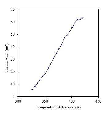 | Figure 8. Variation of thermo-emf (mV) with temperature difference for CdS:CuS composite thin film |
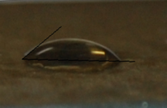 | Figure 9. A water contact angle measurement on CdS:CuS composite thin film surface |
4. Conclusions
- In present paper, we have reported the simple and convenient chemical bath deposition (CBD) method for the synthesisof nanostructuredCdS:CuS composite thin films of thickness 262 nm using cadmium acetate, cupric acetate and sodium thiosulphate in acidic medium. The XRD analysis revealedthat theCdS:CuS composite film is polycrystalline in nature with hexagonal crystal structure with crystallite size around 23 nm.The SEM studies show the uniform and poroushierarchical morphologysuitable for many applications.FTIR analysis explains different bends present inCdS-CuS nanomaterial.The optical direct band-gap energy of film was found to be 2.77 eV.The dc electrical resistivity measurement showsthat the CdS:CuS thin films are semiconducting in nature with activation energy 0.03eV. The measurement of thermo-emf confirms p-type conduction mechanism of CdS:CuS composite thin film. The water contact angle measurement confirms hydrophilic nature of CdS:CuS thin films,which will be suitable for making contact with aqueous electrolytes in electrochemical cells.
ACKNOWLEDGEMENTS
- The authors are thankful to University Grants Commission, for financial support under the project (No: F.47-1695/10 dated 16/3/2011).