-
Paper Information
- Next Paper
- Previous Paper
- Paper Submission
-
Journal Information
- About This Journal
- Editorial Board
- Current Issue
- Archive
- Author Guidelines
- Contact Us
International Journal of Materials and Chemistry
2012; 2(3): 111-115
doi: 10.5923/j.ijmc.20120203.05
Passivation of Porous Silicon by LaF3 Using a Simple Single-Source Chemical Bath Technique
Abdul Al Mortuza 1, Md. Hafizur Rahman 2, Sinthia Shabnam Mou 3, Md. Julker Nain 3, Abu Bakar Md. Ismail 3
1Department of Biomedical Engineering, Gono University, Savar, Banglaesh
2Department of Physics, Pabna University of Science & Technology, Pabna, Banglaesh
3Department of Applied Physics and Electronic Engineering, Rajshahi University, Rajshahi 6205, Banglaesh
Correspondence to: Abu Bakar Md. Ismail , Department of Applied Physics and Electronic Engineering, Rajshahi University, Rajshahi 6205, Banglaesh.
| Email: |  |
Copyright © 2012 Scientific & Academic Publishing. All Rights Reserved.
Passivation of porous silicon (PS) by LaF3 by a novel chemical-bath technique has been investigated in this report. The porous silicon surface has been passivated with LaF3 by reacting LaCl3 with HF in the etching chamber at room temperature. Without removing the porous silicon from the anodizing chamber LaF3 as a result of chemical reaction between LaCl3 and HF was allowed to passivate the PS surface. Several cycles of reaction that gives the various thickness of LaF3 layer on PS have been investigated. The Scanning Electron Microscopy (SEM) on the surface of LaF3/PS/Si structure confirms the LaF3 film deposition on PS layer. The X-ray diffraction (XRD) of the deposited layer revealed a hexagonal nanocrystalline LaF3 deposition. The as-deposited thin (10-cycle) LaF3 layer contained very low concentration of lanthanum (La) and fluorine (F). The concentration of La and F started increasing with the increase in reaction cycle. But the photoluminescence (PL) of as deposited-LaF3 passivated PS was lower than that of fresh PS. Annealing the just passivated PS structure recovered the PL intensity. Experimental results show that the optimized chemical bath passivation process for the LaF3 on porous silicon could enable the porous silicon to be an important material for photonic application.
Keywords: Porous Silicon, Passivation, Photoluminescence, Chemical Bath Deposition (CBD)
Article Outline
1. Introduction
- Porous silicon (PS) has the potentiality to emit visible light and it is expected that this material can be effectively used to fabricate silicon-based visible light emitting devices and optical interconnections. A disadvantage of this material is the aging, that is, the slow spontaneous oxidation of PS[1]. A native oxide layer forms on the surface of the pores and the thickness of this oxide layer grows with time. Due to the aging effect, the structural and optical properties of PS show continuous change with storage time[1]. Passivation of PS is very important for the stabilization and enhancement of room-temperature photoluminescence (PL) of PS.[2]. The surface defects passivation can be achieved from various chemical adsorbates by several techniques[3-5]. In this work, an attempt has been made to grow an epitaxy of Lanthanum Fluoride (LaF3) on PS surface, as a passivation step, aiming to obtain stable and enhanced luminescence of PS layers. LaF3 is a large band-gap (about 10.3 eV)[6] material having a hexagonal crystal structure with a refractive index of1.61[7]. LaF3 thin films exhibit extremely good moisture resistance, therefore they are very useful, e.g., for protecting optical components[8]. As a passivating layer LaF3 has been grown on PS in various ways such as thermal evaporation and e-beam evaporation[9]. Thin films deposited by thermal evaporation are known to possess a columnar microstructure that strongly influences many of their properties[10]. But in this process just prepared PS needs to be transferred to the vacuum coating unit for deposition. Due to extremely high reactivity of the just prepared PS, during this time of drying and transferring the PS to the coating unit oxygen passivation occurs and that is believed to degrade the PL intensity [11, 12]. Moreover it is very difficult to passivate the silicon inside the pores by physical deposition technique. In the quest of finding a way of in-situ passition of LaF3 on the PS so that the PS needs not to be exposed to ambient air before passivation and pores are well passivated, we propose a novel technique quite similar to chemical bath deposition of LaF3. This technique is very simple and contains only one-step. In this CBD of LaF3 technique, LaCl3 is allowed to react with HF which produces the LaF3. When this reaction is done in the PS etching chamber the LaF3 crystallizes on the PS surface and passivates the surface dangling bond of the just prepared PS. This report investigates the structural and optical properties of the novel CBD-LaF3/PS system.
2. Experimental
- Anodic etching was carried out on a (100) oriented phosphorous doped n-type c-Si of 1–2 Ω.cm resistivity using an electrolyte of HF (48%) and ethanol (98%) in 1:1 proportion under a constant current density of 15 mA/cm2 for 30 min at room temperature. The electrochemical anodization of Si wafer was done using a double tank cell set-up as shown in Fig-1. The wafer was cut into pieces and these pieces of Si wafer were cleaned by successively immersing in acetone, ethanol and deionized water. The electrolyte consisted of HF: C2H5OH in the ratio of 1:1 by volume. The etching was done at a current density of 15 mA/cm2. A 100W tungsten lamp was used for illumination from 15 cm distance. After 30 minute anodization, the etching solution and back contact solution was drained out keeping the samples in the etching chamber. The same double-tank chamber in the upright position is used for LaF3 deposition (Fig 2). Fresh HF was then introduced in the chamber to wash out any remaining etching solution on the chamber. After draining out the HF that used for washing, 0.2 M solution of LaCl3 and 48% HF were introduced simultaneously into the etching chamber through the “HF in” and “LaCl3 in” channels to do the chemical reaction.
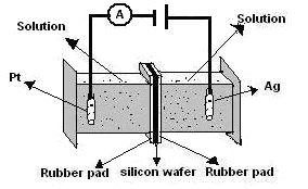 | Figure 1. Schematic drawing of a double-tank chamber for PS fabrication |
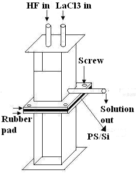 | Figure 2. Double-tank chamber in upright position for chemical bath deposition of LaF3 |
3. Results and Discussion
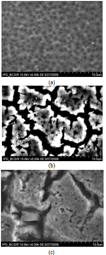 | Figure 3. SEM image of the top surface of (a) 10 (b) 20 and (c) 30 reaction cycles-grown LaF3/PS/Si structure |
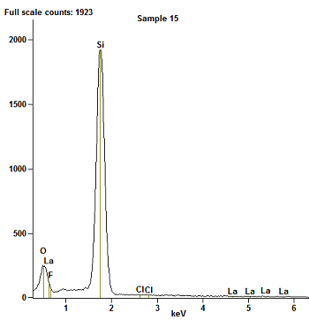 | Figure 4. EDX spectra of 10-reaction cycle LaF3 on PS |
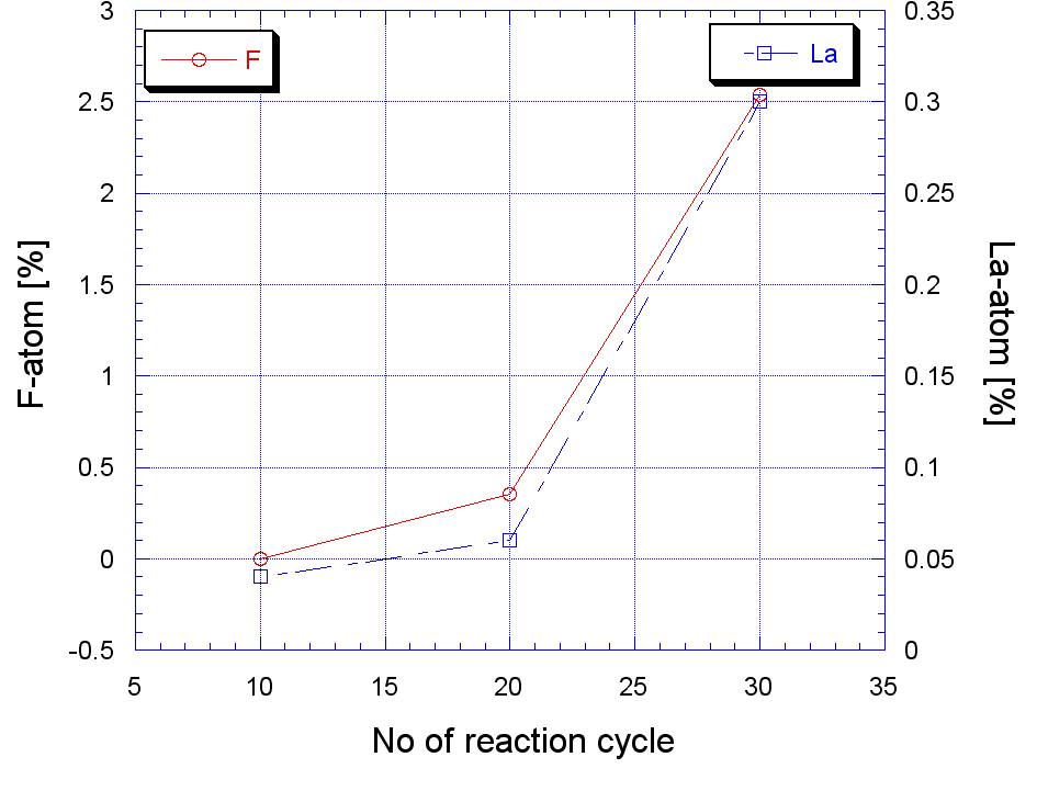 | Figure 5. Growth of La and F |
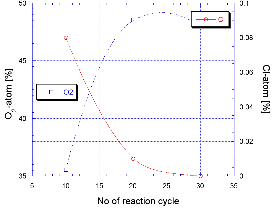 | Figure 6. Growth of oxygen and Cl with reaction cycle |
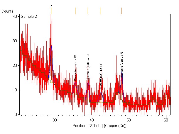 | Figure 7. XRD spectra of as-deposited LaF3 thinfilm |
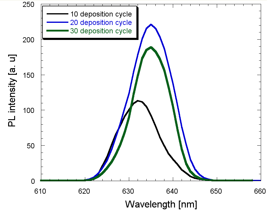 | Figure 8. PL spectra of PS passivated by LaF3 with different reaction cycle |
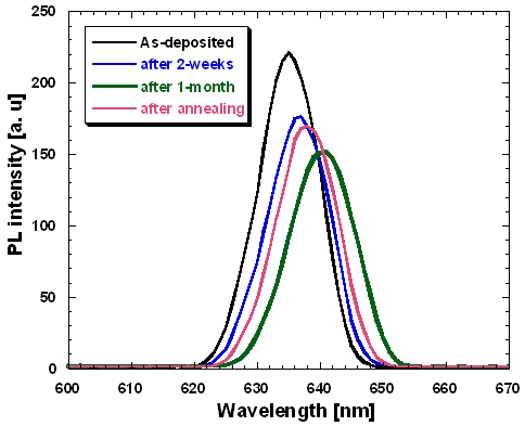 | Figure 9. PL investigation of 20 cycle-deposited LaF3 on PS |
4. Conclusions
- Porous silicon has been tried to passivate with LaF3 deposited by a novel chemical-bath technique that involves only one-step chemical reaction of LaCl3 and HF. The EDX analysis shows that the amount of lanthanum and fluorine increases as the reaction cycle increases. The deposited LaF3 film was amorphous in nature. For a 320 nm excitation the PL peak appeared around 636 nm. The PL showed aging but heat treatment (annealing) could recover the PL intensity due to annealing. It can be concluded that optimized thickness of LaF3 deposited in this novel CBD technique may enable the porous silicon to be an important photonic material.
ACKNOWLEDGEMENTS
- This work has been supported by the TWAS and COMSTEC research grant.
 Abstract
 Reference
 Full-Text PDF
 Full-Text HTML