-
Paper Information
- Next Paper
- Previous Paper
- Paper Submission
-
Journal Information
- About This Journal
- Editorial Board
- Current Issue
- Archive
- Author Guidelines
- Contact Us
International Journal of Materials and Chemistry
p-ISSN: 2166-5346 e-ISSN: 2166-5354
2012; 2(2): 57-64
doi: 10.5923/j.ijmc.20120202.03
Structural, Electrical and Optical Properties of Nanostructured FeCdS3 Thin Films Deposited by Chemical Spray Technique: Effect of Complex
 Abstract
 Reference
 Full-Text PDF
 Full-Text HTML
A. U. Ubale, S. G. Ibrahim
Nanostructured Thin Film Materials Laboratory, Department of Physics, Govt. Vidarbha Institute of Science and Humanities, Amravati, Maharashtra, 444604, India
Correspondence to: A. U. Ubale, Nanostructured Thin Film Materials Laboratory, Department of Physics, Govt. Vidarbha Institute of Science and Humanities, Amravati, Maharashtra, 444604, India.
| Email: |  |
Copyright © 2012 Scientific & Academic Publishing. All Rights Reserved.
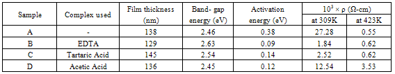
Structural, optical and electrical properties of nanostructured FeCdS3 thin films deposited by spray pyrolysis method using ferric nitrate and cadmium chloride as cationic and thiourea as anionic source with complexes EDTA, tartaric acid and acetic acid is reported. The structural and morphological studies were carried out using X-ray diffractometry (XRD), energy dispersive X-ray analysis (EDS) and scanning electron microscopy (SEM). The X- ray spectrum reveals that the films are nanocrystalline in nature with mixed orthorhombic and hexagonal phase due to FeS2 and CdS lattice. The SEM study shows that the surface morphology of the film is highly influenced by the complexing agent used in the deposition process. Also the optical absorption and electrical resistivity measurements show that the band-gap and activation energy of FeCdS3 thin films varies from 2.45 to 2.63 eV and 0.09 and 0.38 eV respectively depending on the complex used.
Keywords: Thin Films, Nanostructures, Chemical Synthesis, Electrical Properties, Optical Properties
Article Outline
1. Introduction
- Recently preparation of nanostructured materials by cost effective chemical method and investigation of their physical properties is an emerging field of research. The development of nanotechnology is highly influenced by the various chemical and physical deposition processes as the particle size of the nanomaterial is dependent on the deposition method as well as its different preparative parameters. These materials have indeed become a very active research field in the areas of solid state physics, solid state chemistry, materials engineering and medical sciences. The nanostructured materials differ from conventional polycrystalline materials by the particle size that composes them and they show properties that are significantly different from those of conventional material as a result of the large surface area, which controls its bulk properties. If particles have dimensions comparable to the wavelength of electrons, phonons etc., inside the material, quantum mechanical effects plays important role in changing their physical properties especially electrical, magnetic and optical[1]. A blue-shift in optical spectra of quantum-confined particles, and an increase in luminescent efficiency of semiconductors make them suitable for various semiconductor devices. In addition nanostructured materials show lower melting temperatures and higher catalytic activity. The nanostructured materials show potential applications in organic solar cells, rechargeable solid state batteries, fuel cells, molecular electronics, single-electron devices, scanning probes, and sensors[2-6]. Thin films of transition metal chalcogenides particularly Fe and Cd chalcogenides have received much attention due to their importance in photovoltaic and optoelectronic semiconductor devices, as they fulfil some of the requirements that are essential for device fabrication[7-9]. Recently pyrite (FeS2) has attracted attention due to its electronic properties. The p-type pyrite films show n-type conduction after addition of dopants, such as Ti[10], Co[11], Ni[12] and Cu[13]. CdS is another metal chalcogenide, which is most popularly employed heterojunction partner to p-CdTe due to its similar chemical properties useful in achieving high solar conversion efficiencies[14-17]. However, ternary chalcogenide semiconductors Zn1-xCdxSe[18], (HgS)x(Bi2S3)1−x[19] Zn1-xFexSe[20], Zn1-xFexS[21], Cd1-xFexSe[22], PbS–CuxS[23], Bi2S3–CuxS[24,25], Cd1−xZnxS[26–28] have attracted interest of many researchers as their energy gap can be adjusted depending on composition which is useful to improve optoelectronic and photovoltaic characteristics[29]. Wu X. J. et al[30] have prepared Cd1−xFexS thin films by MOCVD and found that with increasing Fe content in the Cd1−xFexS thin films, the conductivity of the films could possibly reverse from n-type to p-type. Although many work on Cd1-xFexS thin film have reported previously, but no reports were available on FeCdS3 or CdS-FeS2 thin films yet by spray method[31,32]. Several chemical techniques have been reported for the preparation of binary and ternary chalcogenide thin films, namely chemical bath deposition[33], spray pyrolysis[34], successive ionic layer adsorption and reaction[35], electrodeposition[36], thermal evaporation[37] and sol gel[38] etc. Out of these techniques, the spray pyrolysis is an economic and popular method as it is simple and safe[39]. One interesting feature of spray pyrolysis is that, under specific conditions the preparation of composite thin films can easily achieved by adjusting the composition of spray solution. From the industrial point of view, synthesis of nanostructured materials at temperature below 773 K by chemical spray pyrolysis method can have wide scope as does not requires sophisticated instruments such as vacuum systems. Generally, the starting chemicals are commonly available metal chlorides and nitrates, which are very cheap. The preparative parameters deposition-temperature, spray rate and solution concentration can be easily optimised to get good quality films.In this paper, we present the synthesis of FeCdS3 thin films using spray pyrolysis method. The effect of complexing agents on structural, morphological, optical and electrical properties of spray-deposited FeCdS3 thin films is been discussed.
2. Experimental Details
- Spray pyrolysis is essentially a thermally stimulated reaction between clusters of ions or atoms of different chemical species. In spray technique a solution (usually aqueous) containing soluble salts of the constituent atoms of the desired compound is sprayed on a substrate maintained at elevated temperatures. The sprayed droplets on reaching the hot substrate undergo pyrolytic decomposition and form a single crystal, cluster, or crystallites of the product. To deposit FeCdS3 thin films onto glass substrates by spray pyrolysis technique ferric nitrate, cadmium chloride, thiourea, EDTA, tartaric acid and acetic acid are used. The film growth rate depends on the number of parameters like temperature of the substrate, duration of spray, the solution spray rate and pH of the solution. The ferric nitrate, thiourea and cadmium chloride powders supplied by Sd-fine Chemicals, Mumbai were dissolved in distilled water to prepare different solutions. The 10 ml volume of 0.1M ferric nitrate, 0.1M CdCl2 and 0.1M thiourea each were mixed directly to get transparent yellowish orange coloured solution of stable phase. In this solution, 10 ml of 0.1M one of the complexing agent from EDTA, tartaric acid and acetic acid was added to prepare spray solution. Finally, the solution was sprayed using compressed air as a carrier gas onto hot glass substrates kept at 453 ±5K temperature. Several trials were conducted to optimize the different deposition parameters such as substrate temperature, spray rate, concentration of zinc acetate etc. The optimized deposition temperature was 453K; the films deposited below this temperature were discontinuous and less adhesive. In addition, the optimized spray rate was found out 6 c.c min -1. All these optimized preparative parameters given in Table 1.
3. Result and Discussion
3.1. Film Deposition
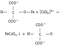
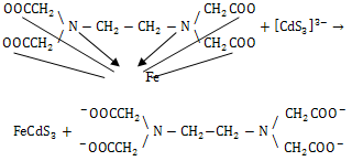
- Cd3+ and S2- ions interact to form[FeCd3]3- anion which attack on Fe3+ ions from spray solution at 453K temperature on hot substrate to form FeCdS3.The growth of FeCdS3 film on hot substrate takes place in two steps.(a) Formation of cadmium sulfide anion:
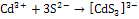 | (1) |
 to produce FeCdS3:
 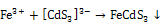 | (2) |
 | (3) |
 | (4) |
 | (5) |
3.2. Structural Analysis
- Figure1 shows the X-ray diffraction spectra of FeCdS3 films deposited using various complexing agents. From the XRD patterns it can be seen that the films deposited using complex tartaric acid are amorphous (sample C), whereas for other complexes films are polycrystalline. Addition of tartaric acid into the spray solution forms iron tartarate complex. The structure of this anion depends upon the ionization level of tartaric acid. The structure of the iron tartarate anion will be different for different ionization levels. For tartaric acid, Fe and Cd complex may be in its fully ionised form, which forms a very strong chelete ring, which thermally decomposes at slow rate that produces amorphous phase of FeCdS3. The EDTA is a powerful chelating agent which forms stable complex with metal ions i.e. Fe-EDTA copmlex which liberates Fe3+ ions at slower rate and provides much time to deposit highly oriented phases in (110) and (203) direction due to FeS2 and CdS respectively. However when acetic acid is used the Fe-actate rpidly decopmoses which produces nanocrystalline phase of FeCdS3. The peaks (110), (020), (120) and (104) are due to orthorhombic and hexagonal phase of FeS2 and CdS respectively. Some additional peakes (210), (110) and (102) are observed when films were deposited wthout complexing agent. The comparison of observed and standard data for FeS2 and CdS is given in Table 2. The grain size of crystallites was calculated by using Scherrer formula,
 | (6) |
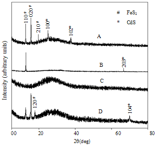 | Figure 1. XRD patterns of FeCdS3 films (A) without Complexing agent, (B) EDTA, (C) Tartaric acid and (D) Acetic acid |
|
3.3. Morphology
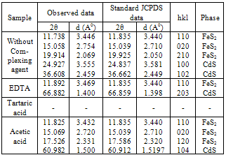
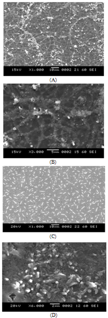
- The SEM micrographs of FeCdS3 films deposited using various complexes are shown in Fig.2. From SEM images, it is observed that the deposited FeCdS3 films are uniform, without cracks with dense surface morphology that covers entire substrate surface area. The SEM images of films deposited without complex and using EDTA shows web-like architecture of FeCdS3 with some irregular grain growth on web structure. Films deposited from tartaric acid complex revealed homogenous dense amorphous morphology with randomly oriented tiny needle like grains. However, the films deposited using acetic acid complex shows vertical rod-like architecture of FeCdS3 nano-grains, which show extremely different morphology as compared to the films, deposited at other conditions. To study stichometry of the film quantitative analysis was carried out using the EDAX technique. Figure 3 shows a typical EDAX pattern of the FeCdS3 film deposited on the glass substrate from acetic acid complex. The elemental analysis was carried out only for Fe, Cd and S; the average atomic percentage of Fe:Cd:S was 22:19:59 showing slight cadmium deficiency.
 | Figure 2. SEM images of FeCdS3 films: (A) without Complexing agent, (B) EDTA, (C) Tartaric acid and (D) Acetic acid |
3.4. Electrical Analysis
- In the present work in order to investigate electrical characteristics silver paste was used to make ohmic contacts to FeCdS3 thin film. The nature of contact was checked up to 30 V by two-probe method. The I-V characteristic of FeCdS3/Ag contacts are shown in figure 4. The I-V characteristics for films are found to be linear which shows that silver produces ohmic contact with FeCdS3.
 | Figure 3. EDAX spectrum of as deposited FeCdS3 thin film |
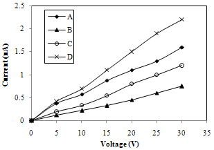 | Figure 4. I-V characteristic FeCdS3 films: (A) without complexing agent, (B) EDTA, (C) Tartaric acid and (D) Acetic acid |
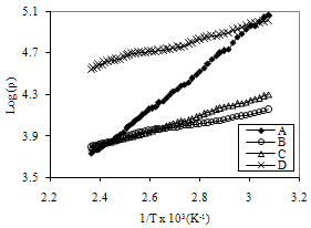 | Figure 5. Variation of Log of resistivity with 1/T for FeCdS3 films: (A) without Complexing agent, (B) EDTA, (C) Tartaric acid and (D) Acetic acid |
|
 | (7) |
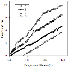 | Figure 6. Variation of thermo emf (mV) with temperature difference for FeCdS3 films: (A) without complexing agent, (B) EDTA, (C) Tartaric acid and (D) Acetic acid |
3.5. Optical Properties
- The optical absorption studies were carried out in the wavelength range of 350 to 910 nm and the absorption spectra is analysed to find band gap energy of FeCdS3. Figure 7 shows the variation of optical absorbance (αt) of FeCdS3 films deposited from various complexes, here ‘t’ is film thickness and ‘α' is the optical absorption coefficient.The variation in absorbance observed is attributed to the film thickness, at what extent film is crystallized, the pinhole free surface and the voids in the film. The film deposited from acetic acid shows more absorbance which may be due availability of more surface area as seen in SEM image.
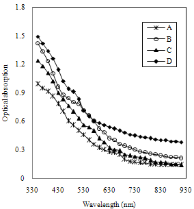 | Figure 7. Variation of optical absorption vs. wavelength FeCdS3 films: (A) without complexing agent, (B) EDTA, (C) Tartaric acid and (D) Acetic acid |
 | (8) |
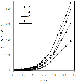 | Figure 8. Plots of (αhν)2 vs. hν of FeCdS3 films: (A) without complexing agent, (B) EDTA, (C) Tartaric acid and (D) Acetic acid |
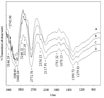 | Figure 9. FTIR spectra of FeCdS3 films: (A) without complexing agent, (B) EDTA, (C) Tartaric acid and (D) Acetic acid |
5. Conclusions
- In the present paper, synthesis of nanostructured FeCdS3 thin films by chemical spray pyrolysis technique with and without complex is discussed. The structural, electrical and optical properties of nanostructured FeCdS3 films were investigated. The XRD pattern suggests that the FeCdS3 films are nanocrystalline in nature with mixed orthorhombic and hexagonal phase of FeS2 and CdS. SEM micrograph shows that, the films deposited using acetic acid and EDTA complex shows vertical rod-like and web-like architecture of FeCdS3. Analysis of UV/VIS spectra of the films reveals that the material is direct semiconductor with band gap in the range 2.45 to 2.63 eV depending on complex used. The thermo-emf measurement confirms that the deposited FeCdS3 films are of n-type. The resistivity of FeCdS3 is of the order of 103 to 104 Ω-cm at 309 K depending on complex used for deposition.
ACKNOWLEDGEMENTS
- The authors are thankful to University Grants Commission, WRO, Pune (India), for financial support under the project (No: F47-258/2007).
References
| [1] | A.J.A. Wirmubst, M.M.R. Boutz., “Superplastic deep drawing of tetragonal zirconia ceramics at 1160°C”,J. European Cer. Soc. Vol. 18, pp.2101-2108 ,1998. |
| [2] | A. Aviram, M. A. Ratner, “Molecular rectifiers”, Chem. Phys. Lett. Vol. 29, pp.277-283, 1974. |
| [3] | F.L. Carter, R.E. Siatkowsky, H. Woliltjen, Molecular Electronics Devices, North Holland, Amsterdam, 1988. |
| [4] | A. Aviram (Ed.), Molecular Electronics Science and Technology, A1P Coiif. Proc, pp. 262, 1992. |
| [5] | A.S. Edelstein and R.C. Cammarata, Nanomaterials: Synthesis, Properties and Applications, Institute of Physics Publishing, Bristol,1996. |
| [6] | Bezryadin, C. Dekker and G. Sclmud, “Electrostatic trapping of single conducting nanoparticles between nanoelectrodes,” Appl. Phy. Lett,Vol. 71, pp. 1273-1275, 1997. |
| [7] | H. Moon, A. Kathalingam, T.Mahalingam, J.P. Chu and Y.D. Kim, “Studies on electrosynthesized zinc mercury selenide alloys”, J.Mater. Sci. Mater. Electron., Vol. 18, pp 1013-1019, 2007. |
| [8] | S.K. Deskmukh, A.V. Kokate,and D.J. Sathe, “Studies on electrodeposited Cd1−xFexS thin films’, Mater. Sci. Eng., Vol. B 122, pp. 206–210, 2005. |
| [9] | R. Chandramohan, T. Mahalingam, J.P. Chu and P.J. Sebastian, Solar Energ. Mater.Solar Cells, “Preparation and characterization of semiconducting Zn1−xCdxSe thin films”, Vol. 81, pp 371–378, 2004. |
| [10] | A. Pascual, P. Diaz-Chao, I.J. Ferrer, , C. Sánchez, J.R. Ares , “the growth and doping of Fe/Ti chalcogenide thin films” Solar Energy Materials and Solar Cells, vol. 87(1-4), pp. 575-582, May. 2005. |
| [11] | I. J. Ferrer, C. de la Heras and C. Sanchez “The effect of Ni impurities on some structural properties of pyrite thin films,” J. Phys.: Condens. Matter., vol. 7, pp. 2115-19, Nov. 1995. |
| [12] | I. J. Ferrer, C. de la Heras and C. Sanchez “Physical properties of Cu-doped FeS2 pyrite thin films,”Appl. Surf. Sci., vol. 70/71, pp. 588-590, 1993. |
| [13] | J. Oertel, K. Ellmer, W. Bohne, J. Röhrich and H. Tributsch, “Growth of n-type polycrystalline pyrite (FeS2) films by metalorganic chemical vapour deposition and their electrical characterization”,J. Crys. Growth, Vol. 198–199, pp. 1205-1210,1999. |
| [14] | C.K. Graetzel and M. Graetzel, “Hydrogen evolution from the photolysis of alcoholic benzophenone solutions via redox catalysis”, J. Am. Chem. Soc. Vol. 101, pp. 7741-7743, 1979. |
| [15] | A. Hagfeldt and M. Graetzel, “Light-Induced Redox Reactions in Nanocrystalline Systems”, Chem. Rev. vol. 95, pp.49-68, 1995. |
| [16] | V.L. Colvin, M.C. Schlamp and A.P. Alivisatos, Nature, “Light-emitting diodes made from cadmium selenide nanocrystals and a semiconducting polymer”, Vol. 370, pp. 354, 1994. |
| [17] | L. Pavesi, L.D. Negro, C. Mazzoleni, G. Franzo and F. Priolo, “Optical gain in silicon nanocrystals”, Nature, Vol. 408, pp. 440-444,2000. |
| [18] | R. Chandramohan, T. Mahalingam, J.P. Chu and P.J. Sebastian, Solar Energ. Mater. Solar Cells, “Preparation and characterization of semiconducting Zn1-xCdxSe thin films” Vol. 81, pp 371-373, 2004. |
| [19] | A.U. Ubale and S.C. Shirbhate, “Electrical, optical and morphological properties of chemically deposited nanostructured HgS–Bi2S3 composite thin filmsJ. Alloys Comp., Vol. 497, pp. 228-233, 2010. |
| [20] | Y.F. Chen, W.C. Chou and A. Twardowski, “Spin-glass-like behaviour of Fe based diluted magnetic semiconductors,” Solid State Commun.,Vol. 96, pp. 865–869, 1995. |
| [21] | A.B. Kashyout, A.S. Aricò, G. Monforte, F. Crea, V. Antonucci and N. Giordeno, Solar Energ. Mater. Solar Cells, “Electrochemical deposition of ZnFeS thin film semiconductors on tin oxide substrates,” Vol. 37, pp. 43–53, 1995. |
| [22] | S. Thanikaikarasan, T. Mahalingam, K. Sundaram, Taekyu Kim, Y.D. Kim and S. Velumani, Adv. Mater. Res, Vol. 68, pp. 69-76, 2009. |
| [23] | P.K. Nair and M.T.S. Nair, “Chemically deposited ZnS thin films: application as substrate for chemically deposited Bi2S3, CuxS and PbS thin films,” Semicond. Sci. Technol., Vol. 7, pp. 239-241, 1992. |
| [24] | P.K. Nair, M.T.S. Nair, A. Fernandez and M. Ocampo, “Prospects of chemically deposited metal chalcogenide thin films for solar control applications,” J.Phys. ED Appl. Phys., Vol. 22, pp. 829, 1989. |
| [25] | V.M. Garcia, M.T.S. Nair and P.K. Nair, “Optical properties of PbSCuxS and Bi2S3CuxS thin films with reference to solar control and solar absorber applications,” Sol. Energy Mater., vol. 23, pp. 47-59, Nov. 1991. |
| [26] | Y.Y. Xi, T.L.Y. Cheung and D.H.L. Ng, “Synthesis of ternary ZnxCd1-xS nanowires by thermal evaporation and the study of their photoluminescence,” Mater. Lett. Vol.62, pp.128-132, 2008. |
| [27] | J.H. Lee, W.C. Song, J.S. Yi, K.J. Yang, W.D. Han and J. Hwang, “Growth and properties of the Cd1-xZnxS thin films for solar cell applications,” Thin Solid Films, Vol. 431, pp. 349-353, 2003. |
| [28] | M.E. Rincon, M.W. Martinez and M. Miranda-Hernandez, Sol. Energy Mater. Sol. Cells, “Structural, optical and photoelectrochemical properties of screen-printed and sintered (CdS)x(ZnS)1−x (0<x<1) films”, vol. 77, pp.25-40, 2003. |
| [29] | S.K. Deskmukh, A.V. Kokate and D.J. Sathe, “Thermal conductivity of BaWO4 single crystal”, Mater. Sci. Eng., Vol. B 122, pp.206, 2005. |
| [30] | X. J. Wu , D. Z. Shen, Z. Z. Zhang, J. Y. Zhang, K. W. Liu, B. H. Li, Y. M. Lu, D. X. Zhao, and B. Yao, “p-type conductivity and donor-acceptor pair emission in Cd1−xFexS dilute magnetic semiconductors,” Appl. Phys. Lett. Vol. 89, pp. 262118, 2006. |
| [31] | N. Badera, B. Godbole, S.B. Srivastava, P.N. Vishwakarma, and L.S. Sharath, “Quenching of photoconductivity in Fe doped CdS thin films prepared by spray pyrolysis technique”, Appl.Surf.Sci., vol. 254, pp. 7042-7048, 2008. |
| [32] | K.W. Liu, J.Y. Zhang, D.Z. Shen, B.H. Li, X.J. Wu, B.S. Li, Y.M. Lu and X.W. Fan, Thin Solid Films, “Growth optical and magnetic properties of Cd1-x FexS films prepared on Al2O3 (0001), Vol.515, pp.8017-8021, 2007. |
| [33] | Elena Rabinovich , Ellen Wachtel and Gary Hodes, “Chemical bath deposition of single-phase (Pb,Cd)S solid solutions”, Thin Solid Films, vol. 517, pp. 737, 2008. |
| [34] | O. Kijatkina, M. Krunks,, A. Mere, B. Mahrov and L. Dloczik, “CuInS2 sprayed films on different metal oxide underlayers”, Thin Solid Films, vol. 431-432, pp. 105-109, 2003. |
| [35] | M. Ali Yildirim, Aytunç Ates and Aykut Astam, “Annealing and light effect on structural, optical and electrical properties of CuS, CuZnS and ZnS thin films grown by the SILAR method,” Physica E: Low-dimensional Systems and Nanostructures, vol. 41(8), pp. 1365-1372, Aug. 2009. |
| [36] | S.M. Pawar , A.V. Moholkar , K.Y. Rajpure, J.H. Kim , C.D. Lokhande and C.H. Bhosale, “Fabrication of Fe:CdSe solar rechargeable (semiconductor–septum) storage cells,” Current Applied Physics, vol. 9, pp. 1122, 2009. |
| [37] | Y.Y. Xi, Teresa L.Y. Cheung, Dickon H.L. Ng, “Synthesis of ternary ZnxCd1−xS nanowires by thermal evaporation and the study of their photoluminescence ,” Materials Letters, vol. 62(1), pp. 128-132, Jan. 2008. |
| [38] | Alessandro Martucci, , Jochen Fick, Serge-Émile LeBlanc, Michael LoCascio, Alain Hach, “Optical properties of PbS quantum dot doped sol–gel films,” Journal of Non-Crystalline Solids, vol. 345-346, pp.639-642, Oct. 2004. |
| [39] | A. U. Ubale and V. P. Deshpande, “Effect of manganese inclusion on structural, optical and electrical properties of ZnO thin films,” J. Alloys Comp., vol.500, pp.138-143, 2010. |
| [40] | A. U. Ubale and D.K. Kulkarni, “Effect of manganese inclusion on structural, optical and electrical properties of ZnO thin films,” Ind. J. Pure Appl. Phy. Vol. 44, pp. 254 -259, 2006. |
| [41] | A. U. Ubale, “Effect of complexing agent on growth process and properties of nanostructured Bi2S3 thin films deposited by chemical bath deposition method,” Mater. Chem. Phy. Vol. 121, pp.555-560, 2010. |