-
Paper Information
- Next Paper
- Paper Submission
-
Journal Information
- About This Journal
- Editorial Board
- Current Issue
- Archive
- Author Guidelines
- Contact Us
International Journal of Materials and Chemistry
p-ISSN: 2166-5346 e-ISSN: 2166-5354
2012; 2(2): 47-50
doi: 10.5923/j.ijmc.20120202.01
Synthesis, Characterization and Dielectric Properties of K1-xNaxNbO3
 Abstract
 Reference
 Full-Text PDF
 Full-Text HTML
S C Bhatt, Manish Uniyal
Department of Physics, H.N.B Garhwal University, Srinagar (Garhwal), 246174,Uttarakhand,India
Correspondence to: S C Bhatt, Department of Physics, H.N.B Garhwal University, Srinagar (Garhwal), 246174,Uttarakhand,India.
| Email: |  |
Copyright © 2012 Scientific & Academic Publishing. All Rights Reserved.
The samples of K1-xNaxNbO3 (X=0.4, 0.2, 0) ceramics (PSN) have been prepared by the conventional solid-state reaction method and sintering process. The prepared samples have been characterized by XRD. All the prepared samples show orthorhombic structure at room temperature. Dielectric and Electrical properties of PSN system have been investigated in the temperature range 450C-2450C, and at 1MHz frequency. It is observed that dielectric constant, loss tangent and electrical conductivity increases with increasing temperature. Near the transition temperature dielectric constant, loss tangent and electrical conductivity of these samples show anomalous behaviour with temperature.
Keywords: Transition Temperature, Dielectric Constant, Loss Tangent, Electrical Conductivity
Article Outline
1. Introduction
- ABO3 Perovskite type materials are of considerable technological importance, particularly with respect to their physical properties such as ferro, pyro-and piezo-electricity, dielectric susceptibility, linear & non linear electro-optic properties etc. The change in physical properties is particularly large when the external conditions, such as temperature, pressure, electric-field, composition etc. are altered. Such effects occur in connection with the simultaneous presence of phase transition in the system, where the atomic structure of the perovskite changes either discontinuously or continuously into another form. The dielectric properties of ABO3 perovskite structure K1-xNax NbO3 for some of the compositions has been extensively studied at high temperature[1] and it shows a number of ferroelectric phases with high spontaneous polarization. The solid solution of ferroelectric KNbO3 and antiferroelectric NaNbO3 exhibits good piezoelectric properties[2,3]. Potassium Sodium Niobate ceramic (K1-xNaxNbO3) with perovskite structures are widely used for transducer applications with broad ranges of technologically important dielectric, piezoelectric, ferroelectric and electro-optic properties. The structure of PSN system at room temperature is basically of the orthorhombic type. K1-xNaxNbO3 (x=0) is a particularly promising ferroelectric with its combination of relatively low dielectric constant ( with extremely high electro-optic coefficients (r42=380pm/V, r33=64pm/V). This makes KNbO3 vary attractive for opto-electronic devices, including high-speed electro-optic switches, modulators, and frequency doublers[4-7]. Dielectric measurements on this material were first reported by Matthias and Remeika [8] and then by Shirane et. al.[9] and observed well defined ferroelectric hystersis loops from room temperature to 4000C, for compositions form about 10 to 100% (mol) of K in K1-xNaxNbO3. Dielectric properties were reported by Narayan Murty et. al. [10]. Cross [11] has predicted, theoretically, the phase-diagram of KNbO3-NaNbO3 mixture from phenomenological arguments. The mixing of NaNbO3 in KNbO3 ceramics play an important role on the ferroelectric Curie temperature, dielectric constant, grain size as well as the planer mechanical coupling coefficient (kp) value [12-13], because NaNbO3 is anti-ferroelectric at room temperature, when mixed with small amount of KNbO3, becomes ferroelectric, which creates interest in the present investigation to investigate this system with a varying composition and temperature range. In this paper, we report the results of investigation on dielectric constant, tangent loss and electrical conductivity of the ceramic system K1-xNaxNbO3 ( x=0.4, 0.2 & 0) prepared by solid state reaction method and sintering process, in the temperature range 450C-2450C, and at 1 M Hz frequency.
2. Preparation
- The starting material was dried at 2000C for one hour to remove absorbed moisture. Different compositions of K1-xNaxNbO3 for (x=0.4, 0.2 & 0) were prepared by weighing the sodium carbonate, potassium carbonate and niobium penta-oxide (starting materials) in proper stoichiometric proportions. The mixture was calcined in the platinum crucible, in air, at 9500C for 2h, for carbonate removal. After cooling, in dry air, the calcined mixtures were weighed to ensure complete carbonate removal.The pre-sintered mixture was ground and pressed into pellets of 10mm diameter. All the pellets were placed on a platinum crucible and sintered, in air, at 10500C for 26 h. The sintered pellets were electroded using air-drying silver paste for dielectric measurements.
3. Characterization
- X-ray powder studies were performed at room temperature with a SEIFERT 3000P X-ray diffractometer using filtered Cu K1 radiation of 1.5405980 A wavelength, in which, Ni, is used as filter. The instrument is well calibrated with silicon standard samples and the lines obtained are matching with the standard lines. At room temperature all PSN ceramic samples exhibit the orthorhombic symmetry. The sub cell parameters were obtained using the auto-X computer software and were compatible with those obtained earlier for ceramics [10,12-17]. The results are summarized in following table.
4. Measurements
- The variation of dielectric constant, loss tangent and electrical conductivity at 1MHz frequency, in the temperature range 450C-2450C have been studied and plotted in Fig. 1, 2 & 3 respectively. These measurements were performed on HP Impedance Analyzer and FLUKE RCL meter, PM 6306.
5. Result and Discussions
- We have measured dielectric constant, loss tangent of K0.6Na0.4NbO3, K0.8Na0.2NbO3 and KNbO3 ceramic pellets using HP Impedance Analyzer and Fluke RCL meter PM 6304, at the temperatures from 450C to 2450C.The temperature dependence of dielectric constant, loss tangent and conductivity at 1MHz have been shown in Figs 1, 2 & 3, and tables-1,2 & 3, respectively.From these figures (Fig.1-3) and tables (Tables 1-3), it is observed that the mixed system of K1-xNaxNbO3 has a transition from orthorhombic to tetragonal at about 2200C. It is 2250C for KNbO3, 2150C for K0.8Na0.2NbO3 and 2050C for K0.6Na0.4NbO3, which shows that transition temperature from orthorhombic to tetragonal shifts towards lower temperature as we increases the quantity of anti- ferroelctric material sodium niobate in the mixed system of K1-XNaXNbO3, which is in agreement with previous observations[1,18]. Lattice parameters of K1-XNaXNbO3 for different compositions at room temperature have been shown in table-A, which shows a decrease in lattice parameters as we add antiferroelectric material NaNbO3 in mixed system of K1-xNaxNbO3 ceramic.
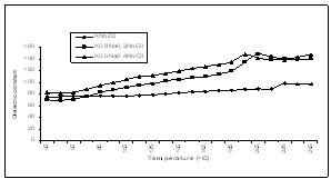 | Figture 1. Variation of dielectric constant with temperature for K1-xNaxNbO3 at 1 MHz |
|
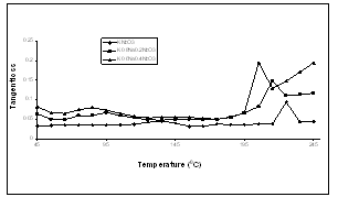 | Figture 2. Variation of tangent loss with temperature for K1-xNaxNbO3 system at 1 MHz |
|
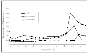 | Figture 3. Variation of electrical conductivity with temperature for K1-xNaxNbO3 system at 1 MHz |
|
6. Conclusions
- Our results shows that the mixing of Na is effective in promoting the densification of the ceramics and can be well sintered and exhibit a dense, pure perovskite structure and this is attributed to the fact of the presence of oxygen vacancies. For most KNN-based solid solutions, the piezoelectric properties are enhanced but with a reduced Tc [19]. Therefore as 20% mixing of Na, transition temperature is 215oC whereas 40% mixing of Na, transition temperature reduces to 205oC, which shows that transition temperature from orthorhombic to tetragonal shifts towards lower temperature as we increase the quantity of anti - ferroelectric material NaNbO3 in the mixed system, K1-XNaXNbO3.
ACKNOWLEDGEMENTS
- The authors are thankful to IIT Delhi, NPL Delhi & IIT Roorkee for library facilities and Material Science Research Centre. IIT Madras, for providing laboratory facilities for sample preparation and characterization.
References
| [1] | Singh K, Lingwal V, Bhatt S C, Panwar N S & Semwal B S,2001, Material Research Bulletin, 36,365-2374 |
| [2] | Ahn C W, Song H C et.al.,2005, Japanese Journal of Applied Physics, 44,1361-1364 |
| [3] | Ahn C W, Choi C H ,2008, Journal of Material Science, 43,6784-6797 |
| [4] | Holman R L, Althouse Johnson L M & Skinner D P,1987, Opt Eng 26, 134 |
| [5] | Nystrom M J, Wessels BW, Chen J & Marks T J,1996, Appl Phys Lett 68,761 |
| [6] | Hoerman B H, Jichlos B M, Nystrom M J & Wessels B W,1999, Appl Phys Lett 75, 2707 |
| [7] | Maeder M D, Damjanovic D, Setter N,2004, Journal of electroceramics 13,385-392 |
| [8] | Matthias B T, Remeika J P,1951, Phys Rev 82, 727 |
| [9] | Shirane G, Newniham R & Pepinsky R,1954, Phys Rev 96(3), 581 |
| [10] | Narayana Murty S, Ramana Murty K V, Umakanthan K & Bhanumati A,1990, Ferroelectrics, 102, 243 |
| [11] | Cross L E,1958, Nature, 181, 178 |
| [12] | Lin D , Kwok K W and Chan H L W,2007, Journal of Applied Physics 102, 074113 |
| [13] | Chu S Y, Water W, Juang Y D & Liaw J T,2003, Ferroelectrics, 287, 23-33 |
| [14] | Natl. Bur Stand, (U.S.) Monogr.1980, 25, 17, 62 |
| [15] | Katz L & Megaw H D,1967, Acta Crystallogr, 22, 639 |
| [16] | Wood E A,1951, Acta Crystallogr. 4, 353 |
| [17] | Hearthing G H,1967, J Amer Cerm Soc, 50,330 |
| [18] | Shirane G, Newnham R & Pepinsky R, 1954, Phys Rev 96,581 |
| [19] | Sun X, Chen J et.al,2009, J.Am.Ceram. Soc., 92[1] 130-132 |