-
Paper Information
- Paper Submission
-
Journal Information
- About This Journal
- Editorial Board
- Current Issue
- Archive
- Author Guidelines
- Contact Us
International Journal of Internet of Things
2017; 6(3): 106-148
doi:10.5923/j.ijit.20170603.03

IoT Applications in Future Foreseen Guided by Engineered Nanomaterials and Printed Intelligence Technologies a Technology Review
 Abstract
 Reference
 Full-Text PDF
 Full-text HTML
G. K. Moinudeen1, F. Ahmad2, D. Kumar3, Y. Al-Douri4, 5, S. Ahmad3
1CII, Gurgaon, Haryana, India
2IRIS Worldwide Integrated Marketing, Gurgaon, Haryana, India
3YMCA University of Science and Technology, Faridabad, Haryana, India
4Nanotechnology and Catalysis Research Centre (NANOCAT), University of Malaya, Kuala Lumpur, Malaysia
5Physics Department, Faculty of Science, University of Sidi-Bel-Abbes, Algeria
Correspondence to: S. Ahmad, YMCA University of Science and Technology, Faridabad, Haryana, India.
| Email: |  |
Copyright © 2017 Scientific & Academic Publishing. All Rights Reserved.
This work is licensed under the Creative Commons Attribution International License (CC BY).
http://creativecommons.org/licenses/by/4.0/

The impact of ‘engineered-nanomaterials’ in cost effective fabrication of micro/nanosensors, and on site energy harvesting devices using ‘printing technology’ for Internet of things (IoT) applications has been assessed in this technology review after analyzing the ongoing progresses reflected in market research forecasts and the anticipated future projections.Being actively involved in the study of ‘engineered nanomaterials’ using inorganic, organic, and biomolecular building-blocks for improving the characteristics of microelectronic/microsystems (MEMS/NEMS) based sensors/actuators, theoretical/experimental studies of 1, 2, and 3D nanomaterials along with the developments of low-cost printing technology for fabricating the electronic/optoelectronic devices and circuits on plastics, paper, and textiles, an attempt has been made in this review to examine the impact of these novel nanomaterials and their printing technology to enhance the capabilities of the related enabling technologies of IoT applications. Novel designs of supra molecular nano-building-blocks to realize hierarchically organized molecular complexes responding to single/multi stimuli with additional electronic intelligence realized by low-cost printing of sensors and actuators along with the wireless connectivity on flexible substrates in the background, possible answer for meeting the gigantic requirement of trillion devices by 2020 has been searched in this study. Combining the cost effective printing of active devices using polymeric molecules with known electronic/optoelectronic transport properties and 2D-layered materials like graphene and other graphene like materials, is found promising to pursue by addressing to the problems of compatible patterning for devices/circuits fabrications. A number of practical issues are discussed in which the basic concept of ‘materials by design’ is foreseen to play a major role in the coming times. Biomimetically produced supra molecular-complexes deserve special attentions for realizing printed sensors/actuators/devices and interfaces to generate big-data for cloud based decisions initiating local control actions better in IoT proliferations in future.
Keywords: Internet of Things (IoT), Sensors, Nanomaterials by design, Printed intelligence, Biomimetic Material synthesis
Cite this paper: G. K. Moinudeen, F. Ahmad, D. Kumar, Y. Al-Douri, S. Ahmad, IoT Applications in Future Foreseen Guided by Engineered Nanomaterials and Printed Intelligence Technologies a Technology Review, International Journal of Internet of Things, Vol. 6 No. 3, 2017, pp. 106-148. doi: 10.5923/j.ijit.20170603.03.
Article Outline
1. Introduction
- The syntheses of nanomaterials using novel paradigm of ‘materials by design’ involving inorganic, organic/polymeric, and biomolecular building blocks that are chemically conjugated through strong and weak interactions have already started showing ‘smart’ and ‘intelligent’ functionalities in form of proof of concept [1, 2]. Further extensions of the capabilities of these nano building blocks are anticipated in preparing supramolecular hierarchical architectures appropriate for a number of applications. Adding molecular recognition based self-assembly initiated conjugation properties resulting in topology dependent self-organizing behavior are found to mimic the Nature by acquiring the desired physico-chemico-biological features. These developments would certainly introduce more novel applications in near future meeting intelligent material requirements [3, 4]. A variety of self-correcting features, autonomously applied to the undesirable changes caused by externally influences, are getting introduced in new materials possessing self-healing, self-cleaning, and many more features that have already started appearing on the horizon of R&D to mature for industrial applications [5-7]. These kinds of nanomaterials with programmable physico-chemico-biological properties are expected to influence the huge demand of generating, mining, and analyzing the ‘big-data’ arising from the Internet of things (IoT) applications [8]. It is quite likely that the fast-growing developments of smart and intelligent materials might ultimately enable sharing part of the cloud computing based decision making loads of the IoT by distributing the decision-making and action-taking activities locally among the sensors and actuators interconnected throughout. This would enable more efficient use of the cloud resources in organizing other related activities of integrating the large number of smart objects predicted to reach a trillion in number by 2020 [9]. While employing a large variety of engineered hybrid nanomaterials for meeting application-specific responses in abundance, it is quite possible to minimize or eliminate the toxic effects arising from using these synthetic materials in all-pervasive IoT applications involving human beings by employing biomolecular species derived from natural sources like plants. It is further becoming more pertinent to evolve greener methods of synthesizing these nano building blocks from natural materials of plant origin comprising of almost unlimited varieties of phytochemicals that are evolved through millions of years in Nature for minimizing their cytotoxicity [10]. Employing biomimetically motivated green material syntheses and developing hybrid nanomaterials by conjugating nano particulate inorganic, organic and biomolecular species would enable minimizing the inorganic part required for some specific purpose in addition to increasing the biomolecular part with the appropriate combinations of polymeric components of organic origin. This would allow incorporating the features of soft materials with added advantages of green smart/intelligent compositions possessing minimum toxic properties. Ideally, once this strategy of optimizing the material composition is mastered using computer aided designs involving quantitative structure activity relation data (QSAR), already compiled for a very large number of materials at atomic and molecular levels, mimicking some features of the living organism, would not remain a far-fetched dream [11-14]. What Nature took so long might be possible to mimic with the help of supercomputers based designs in a relatively much shorter duration while synthesizing newer compositions that would be smart/intelligent as well as green in nature. This would especially turn the entire ecology smart and intelligent resulting in better living conditions. Addition of these materials in realizing components, devices, and systems for their uses in the all-pervasive applications of IoT is indeed expected to make a number of significant changes in near future as a whole [15]. The ever-increasing demand put on cloud hub of IoT applications would certainly necessitate providing matching kind of ‘electronic intelligence’ using the existing foundries of very large-scale integrated circuits (VLSICs) and micro-electromechanical systems or microsystems technologies (MEMS/MSTs). Taking into account all these fast growing designs of future nanomaterials and their applications in responding to external stimuli, it would make the whole IoT applications more flexible while organizing their roles in addition to distributing the tasks of the sensors and actuators with the help of built-in material intelligence already suggested. Possibly, adopting the ‘More than Moor’s’ approach with addition of ‘clever’ integrations of functionalities might offer a better solution over and above the existing scaling down of the device dimensions of VLICs. This might involve shifting to vertical integration of devices and functionalities along with deploying parallel processing based implementations to move ahead in future. And all these changes must be made at affordable cost by deploying functional materials as ink for printing devices and circuits on polymeric flexible substrates including papers and textiles as well. In this context, the concept of 0, 1 and 2-dimensional nanomaterials will not only help in reducing costs but also incorporate functionalities with more flexibilities in varying the fundamental properties of electrons and holes as charge carriers. Currently, these possibilities are being demonstrated well in a number of 2D materials including graphene along with an ever-growing family of other layered/non layered materials that are currently being studied as they appear better suited to convert them into active material inks for printing metal, semiconductor and insulator components. It would, thus, be easier to realize low-cost flexible electronics to provide electronic intelligence somewhat similar to living organisms aided by the existing VLSI systems already in vogue [16-20].Development of functional nanomaterials for preparing hierarchical molecular complexes responding to multiple stimuli would partly compensate for further extensions of VLICs and MEMS/MST activities up to certain extent. Moreover, this ongoing development of ultraminiaturized devices and circuits is currently reaching its theoretical limits. Further developments do need complementary supports from other areas of innovation. Large scale and large area printed intelligent systems and displays using smart and intelligent nano inks will be possible without cost intensive investing in mask making and patterning facility [20, 21].Another important aspect in connection with the success of IoT applications lies in taking care of the energy consumptions of the sensors that are remotely located and difficult to interface with existing power lines. No respite is currently foreseen to meet the projected energy demands growing enormously with continuously increasing population of interconnected information-gathering devices that are expected to reach to ‘trillion’ by 2020. Only viable solution, foreseen feasible in this context, is to improve the conversion efficiency of solar photovoltaic (SPV) devices and their ruggedness such that they are deployed locally to generate sufficient energy to meet the requirements adequately. In this context, the emerging ~21% efficient perovskite solar cells appear to offer better option. Of course, the stability and useable life of these devices are certainly expected to settle down in near future as it happened in the case of silicon and other materials in the last six decades. Addition of 2D-perovskites and lamellar mono crystalline materials having enhanced photosensitivity, reasonable carrier lifetimes and higher charge carrier mobility are the future hopes on which currently made efforts are hinging to improve the efficiency closer to or if possible exceeding its theoretical limits. The alternate approach of tandem configuration of PVSCs along with spectral splitting for optimal PV conversion by a combination of suitable materials instead of only one is practically being aimed at for ~50% efficient conversion of solar radiation into electrical energy for developing mini-panels with affordable investments [7, 22, 23].The main objective of this review is to examine the extent to which these anticipated advantages are possible to achieve in future IoT applications as evidenced in currently emerging system performances reported or published. Single/multi stimuli responsive engineered nanomaterials possessing smart and intelligent features would collect environmental data without external power sources for monitoring themselves autonomously with wireless connectivity. Numerous IoT applications are being translated into the businesses as noted by M/S Allied Market Research (AMR) in their report projecting market to grow @ 15% annually in revenue generation of ~ US$70 billion by 2022. Smart material applications in ‘Market Research Projects’ include sensors, actuators, motors, structural materials, and several types of novel coatings to name a few. Driven by the potential end-users, the market could further be segmented into industrial, consumer electronics, healthcare, retail, automotive, and many more like that. The observations made by ‘eSafety Forum’ are worth mentioning in this context. They concluded from the data available that on average one third of the serious road accidents are generally caused by driver’s fatigue. A ‘Harken Project’ was initiated for improving driver’s safety by developing embedded non-intrusive sensors for assessing cardiac and respiratory functions. Integrating sensing materials into safety belts and seat covers of the cars could thus detect the heartbeats and the respiratory conditions of the driver by eliminating the noise due to moving vehicle generated vibrations, and the body movements. The ‘Harken’ system monitors the fatigue-related physiological activity of the driver by identifying the changes in breathing and heart rates to anticipate and prevent car accidents related to fatigue by timely alerting the driver. Another European supported ‘Graphene Flagship’ program succeeded in developing graphene ink for fabricating sensors for measuring the parameters like temperature, humidity, pressure, and light by printing an electronic circuit onto an RFID tag. The low energy consumption and the ability to support high data speeds achievable from these sensors would certainly make the graphene a more useful material for new communication technologies like 5G for IoT applications [24].Applying graphene ink onto cotton to produce a conductive textile is foreseen in contrast to the existing wearable sensors relying on the rigid electronics mounted on apparel textiles. This new ink-impregnated cotton fabric being interactive is also breathable, comfortable to wear, and washable while retaining textile electronics. These smart clothes have potentials in sports and health related products replacing wrist wearable devices like ‘fitness tracker’ and ‘heart rate monitor’. Similarly, ‘Hexoskin smart shirts’, for example, are capable of monitoring heart and breathing rates, steps and pace, acceleration, the intensity of the sporting activities and also the sleeping positions. The fabric is machine-washable, breathable, and odor-free besides providing UV-protection. Hexoskin connected Health Platform and data analysis software for health research are currently in use in clinical development, sports, and fitness projects [25].Bristol University reported developing a self-healing compound for airplane wings and fuselage. This self-healing carbon skin is coated with a thin layer of nano sensors that measure pressure and temperature, which, in case of getting damaged due to stone chips or bird strikes, sends a signal to activate uncured material within the nano crystalline structures to start curing the damaged area like an adhesive heals a crack. These materials would be usable in bike helmets, golf clubs, tennis racquets, fishing rods, and even nail polish and cracked mobile phone screens [26]. Such smart garments are already available in the market although most smart material technologies are still at R&D stage. Small and medium enterprises currently lack the adoption of smart materials due to their higher costs, according to the AMR study. But the researchers estimate that with several governmental initiatives and programs as well as the increasing demand for smart materials from industries like construction, manufacturing, and automotive would be driving the market in the coming years [27].
2. Engineered Nanomaterials for Intelligent Sensors and Actuators
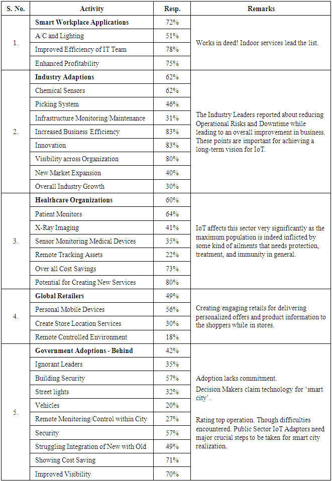
- Although, the IoT term came into existence about two decades ago, however, a common acceptable definition is not yet settled among the businesses adopting it. Almost 98% of the respondents (e.g. claiming to understand IoT) offered widely varying descriptions. For instance, 67% of the respondents considered IoT to add ‘Internet Connectivity’ to everyday objects. This may perhaps be the leading definition of IoT from research angle, but it certainly differs from the one proposed by Kevin Ashton, who coined the term ‘Internet of Things’ in 1999 [28]. Others claim that IoT includes a network connecting multiple objects, for instance, devices and sensors (65%); a platform to connect industrial components (55%); automating building services (52%), and using wearable technology (46%). Whereas, Ashton made it explicit that the IoT means sensors connected to the Internet that behave in an Internet-like way by making open ad-hoc connections, sharing data freely, and allowing novel applications, so computers could understand the world around and become humanity’s nervous system. IoT has already started showing its advantages and applications accordingly right from its start. In order to have a glimpse of how various socio-economic groups are responding to IoT adoptions in their areas of activities, a very useful survey was conducted recently and the responses received are compiled in Table 1 [29].
|
|
2.1. IoT - Making Everything Intelligent
- Growing impact of information and communication technologies (ICTs) combined with low-cost production of smart/intelligent subsystems/systems has started improving the performance of various enterprises. This is also affecting even day-to-day activities particularly in relation to overall improvement in the quality of life by introducing functionalities aided by the recent developments. Engaging a large number of computers in this context is primarily based on standard and inter-operable communication protocols that are not only capable of identifying the physical as well as virtual objects but also involved in integrating their attributes into the information network. Dynamically self-configuring global IoT network has started penetrating deep into the surrounding environment along with consumer goods as the ‘things’ comprising of electronic devices endowed with the capabilities like localized recognition, computing, and communication providing object-level tracking. Accordingly, subsequent to the past two major developments in the field of computers followed by the introduction of ‘Internet’ in the recent past; the IoT is certainly emerging as the next revolutionary force driving the development of ICT much ahead. It is not difficult to foresee the stronger impacts of IoT by counting the current level of usage of nearly 1.5 billion personal computers (PCs) and over 1 billion cell-phones connected to the Internet along with the anticipated number of devices to go well beyond 100 billion by 2020. All these features, put together collectively, are bound to influence the emerging markets generating over 40 times bigger impact as a whole compared to that produced by ‘Internet Technology’ as assessed [30-32].
2.2. The Enabling Technologies
- The fast-growing interest in IoT applications comes from full access to a number of constituent enabling technologies that are being developed under different disciplines at their own pace and are put to use in IoT, where the electronic functionalities have been playing crucial roles. These basic enabling technologies are described below to highlight their impacts on IoT covered in more detail in the references cited [33-44].
2.2.1. The Wireless Communications
- Short/long-range wireless communication channels covering ranges from a few centimeters to a few meters (e.g. in personal area network); and to hundreds/thousands of meters in local and global area networks, respectively, are playing dominant roles in ongoing IoT development. Wi-Fi is the common term used in wireless local area networking of devices employing IEEE 802.11 standards. Wi-Fi devices used in Wi-Fi (2.4/5GHz Radio Band WLAN network) include a variety of personal computers, laptops, video-game consoles, smartphones, digital cameras, tablets, digital audio players, and modern printers, besides many others in offing. These devices are Internet connected having a wireless access within the range of ~ 20 meters indoors but even greater than in outdoors. The technologies including Wi-Fi, Bluetooth, and IR, are certainly the backbones of data transfer among smart devices deployed as nodes at different levels.A distributed arrangement of sensor and actuators in a wireless sensor actuator network (WSAN) has been gathering data about the physical environment for sending the same to the controllers/actuators through single/multi-hop communication system, wherein, the controllers/actuators act in changing the behavior of the environment or physical systems within certain limits [45]. It has thus become possible to remotely control the distributed interactions taking place within the physical world. Depending upon the nature of the target application, the WSAN nodes are either stationary or mobile. Sensor nodes are generally stationary, whereas the actuators are mobile such as in robots and unmanned aerial vehicles (UAVs). Sensor nodes are usually low-cost and low power consuming miniature devices with limited sensing, data processing, and communication capabilities, whereas the actuator nodes possess stronger computation and communication features with higher energy consumption and thus always put more constraints. WSANs are different from the wireless sensor networks (WSNs) involving new generations of sensor networks though there are quite a few common features including the reliability, connectivity, scalability and energy efficiency. Coexistence of sensors and actuators in WSANs makes the major difference between these two networks. WSANs have the ability to change the physical world, but not the WSNs. In WSNs, the power consumption is of primary concern. However, this may be for meeting the real-time, reliable communication requirements in WSANs. There are situations where only WSNs are required, e.g. environment and product quality monitoring. The number of applications is continuously growing requiring actuators along with sensors wherein the network interacts with the physical system or the environment. WSAN applications include disaster relief operations, intelligent buildings, smart homes, smart spaces, and pervasive computing systems [46-58]. WSANs employ the feedback control systems comprising of sensors and actuators. This is the reason that WSANs are forming the backbone of many applications providing an excellent distributed control system in contrast to wired solutions. For instance, WSANs allow more flexible installation and maintenance, fully mobile operations, and monitoring and control of equipment in hazardous and difficult-to-access environments at relatively affordable costs [49, 51, 59-61]. Generic design of platform independent WSAN was reported promising results for its implementations [54].
2.2.2. The Sensors and Actuators
- Sensors provide information related to the environmental parameters around a monitoring unit along with their variations with the help of appropriate transducers. The measured parameter variations are transferred to data collection for further analytics and applications. Some important features of IoT sensors are discussed here briefly.The current theme of examining the influence of engineered nanomaterials and printed intelligence becomes more pertinent in case of sensors and actuators that form the backbone of IoT data collection applications. In this context, a number of features of these devices are seen to depend on various features mentioned in the following.MEMS/NEMS fabricated using micro/nano mechanical components by modified CMOS IC technology and anisotropic etching of silicon, respond to a number of physical, chemical and biological measurands resulting in a new class of sensors and actuators with unprecedented precision, sensitivity and resolution. Particularly, Si based MEMS/NEMS platforms (also called micro system technology (MST) and micro machines in Europe and Japan, respectively, [62-68] are well suited for integration of CMOS signal conditioning and processing circuits along with. Syntheses of nano particulate inorganic, organic, polymeric, and biological species conjugated to prepare hybrid nano materials with size and shape specific physico-chemico-biological properties possessing stimulus responsive behavior are expected to improve the capabilities of these devices further. In addition, biomimetic synthesis of materials in combination with MEMS/NEMS based sensor platforms are expected to result in intelligent features derived from molecular recognition based self-regulated processes and configurations of nano species providing large-scale green processing suitable for production. Moreover, low cost printing using engineered nano inks would produce sensors, actuators, and electronic circuits on rigid, flexible or uneven surfaces including low cost substrates like plastic sheets, paper, and textiles. Finally, intelligent packaging of sensors, actuators and signal conditioning/processing circuits would enhance the usage of sensor/actuator technology resulting in material savings due to timely consumptions prior to their degradations because of external environmental conditions. The precision, accuracy and sensitivity of the current nanosensors have been enhanced significantly in areas involving MEMS/NEMS components. Further, introducing engineered nano materials has the potentials to add another new dimension to the whole sensor technology, where hybrid nanomaterials in 1, 2 and 3D are offering unprecedented sensitivity, selectivity, and resolution via their topology specific physico-chemico-biological interactions resulting in single/multiple stimulus responsive molecular complexes. Nanoparticulate forms of inorganic, organic, polymeric, and biomolecular species combined with MEMS/NEMS device structures are opening numerous novel possibilities not foreseen earlier. Addition of 2D materials (i.e. graphene and graphene like many others) is another area, which is getting explored fast, adding still more potentials to these engineered nano materials for their sensor/actuator applications in particular [69].Processes used for introducing engineered hybrid nanomaterials in MEMS/NEMS are, in general, carried out in solution form, which is bound to reduce the costs once the involved technologies mature. Out of several options, printed nano sensors with intelligence are making revolutionary changes in this context as foreseen in future IoT applications.Going by the conventional way of environmental parameters assessments using commonly available sensors, it may be quite expensive with many physical limitations including constrained modifications involving lengthy procedures. However, with the recent advances made in engineered nano materials, a large number of alternatives are emerging fast that are expected to overcome these constraints by changing the sensor modality. Because of flexibility provided by a large variety of nano sensors available today, a given sensor meant for measuring a particular parameter could instead be used for a different purpose, while answering the same end-question via a low cost route. This was demonstrated by employing a temperature sensor to replace flow meters in pipes and mechanical switches in refrigerator doors, thus changing the modality of the temperature sensor from measuring the room temperature to measuring other physical parameters [70]. Current market research has been linking the growth of the MEMS/NEMS market to the increasing demands arising out of monitoring/control requirements of the environment and in developing better equipment and instruments. With increasing number of sensors deployed in cars, industrial equipment, installations, and ambient intelligence, it is certainly going to demand higher production of sensor and actuators consequently. Keeping in view their uses as well as overall reliability, such sensors must be self-sustaining while using wireless communication in their system networking [71]. A wireless local-area network (LAN) uses RF energy in contrast to the wired network for connecting devices like laptops, printers, and similar others to the Internet, and business networks. The simplest wired networks use ‘Ethernet’ ports on the network router and the computer/other devices. Although wired networks, at some point of time in past, were considered faster and more secure than wireless networks, but of late, the situation has reversed with improved wireless networking standards and technologies resulting in speed and security in the intervening period. There are reasons to replace wired network with wireless network, for instance, to incorporate added mobility to network resources from any locations within the coverage area ultimately affecting productivity besides ease in operation and expansion. Even robust security is available at lower cost because of no additional investment in cable laying for interconnections as in the wired networks [71]. The ever-increasing number of future devices required is currently the driving force behind introducing further overall miniaturization in the devices to reduce power consumptions, and provide effective communication networks besides convenient packaging along with their system integrations. Instead of sourcing a number of sensors from a large capacity power supply, it is preferred to provide for local energy harvesting modules along with their associated wireless communication networks individually [72,73]. MEMS/NEMS sensor applications are proliferating more in human health care sector with the growing population of the elderly citizens requiring medical care through medical infrastructures globally. For cost-effective healthcare accessible to more number of people at affordable costs, the hospitals/healthcare facilities must be established at reduced costs by improving the overall efficiency without sacrificing the quality. Hospitals are being motivated to find innovative ways to meet this objective. Consequently, a centralized medication distribution system has been emerging as a standard model, but more facilities are also switching over to a hybrid or decentralized distribution model. There is also a growing trend in transferring general medical test facilities from a fully equipped central laboratory to smaller units, which are closer to the patients needing them. This leads to growing demands of small and affordable diagnostic devices, especially for point of care type of applications using ‘laboratory on a chip’ type facility [74]. In addition, the rising concern for National Security is another factor needing serious attention for combatting the terrorist threats and outbreaks of infectious human or animal diseases. This would facilitate developing portable multi-parameter measuring instruments to test atmospheric contaminations including air, water, and foodstuffs as well as human blood for microbial attacks in case of emergency [75, 76]. Another reason for exploring MEMS/NEMS technology is for adding a ‘clever factor’ in mitigating the limitation due to imminent terminus of the Moore’s law. The IC industry is bound to look for other ways to improve the performance of their circuits and systems. The emerging ‘More than Moore’ concept is expected to add new technologies to 2D-landscape of the current microelectronic devices and circuits to incorporate additional functionalities via vertical integration using die stacking [77]. Besides, more flexible and more affordable production technologies are also emerging driven by the possibility of producing lower cost, and larger surface area devices like solar cells, displays, wearable electronics and disposable diagnostics devices [78]. Modified printing technology is one alternative besides using low cost substrates like plastics, paper, and textiles in printing intelligence at lower cost. This is to complement the existing VLSIC capabilities better. Eventually, a large number of nano-enabled products will emerge from future R&D investments [79]. The current market trend is progressively relying upon merging of functionalities in products like cameras, music systems, computers, mobile phones, and portable consumer electronics as well as the merger of MEMS/NEMS technologies with VLSICs. In this context, there are examples of MEMS/NEMS being introduced into portable electronic products comprising of silicon-based microphones and liquid lenses for autofocus and zoom options [80, 81]. Similar pressures are being felt from ever-increasing demand of large memories of higher capacities with embedded or stand-alone types [82, 83]. It is significantly important to note that the increasing use of sensors and other miniaturized electronic devices is gradually shaping the environment available for intelligent interactions through IoT. For this to happen, stronger needs are emerging for low cost miniaturized devices and subsystems, which are energy efficient and self-sustaining as well as able to communicate wirelessly with other electronic devices and subsystems used as ‘smart dust’. These smart dusts comprise of large number of MEMS/NEMS/MST based sensors, robots, or similar other devices, that can detect light, temperature, vibration, magnetic field, and chemicals to name a few, and are operated through computer network while distributed over certain specific area for sensing through RF network [84]. The wireless sensor networks are exploring to incorporate sensors even in previously inaccessible locations. It is also becoming feasible to use a large numbers of sensors because there is no longer the need for their regular replacement or recharging their power sources [85]. MEMS/NEMS offer special advantages in contrast to commonly used counterparts available commercially. Adding few special etching, bonding and assembly techniques to common CMOS IC fabrication, it has been possible to produce them without much of alterations in process lines. Although MEMS/NEMS have grown extensively in the past decade, many challenges are still there in terms of their fabrication, packaging, and applications and upcoming solutions of these challenges will determine the commercial success of these devices both in technical and economic terms [86]. In a typical MEMS based human health care system, a clear shift from the clinical to point of care diagnostics is noted with a slow but significant changeover from medical diagnostics to more lifestyle oriented tests of allergy, drugs, cholesterol, alcohol, and sport injuries. These additional application areas put together make the MEMS market more consumer-oriented. Perhaps the fastest growing market for MEMS/NEMS with many interesting applications especially includes ‘Point of Care’ monitoring in which glucose level monitoring could be cited as one of the largest single segment. But there are also many niche areas like: retinal implants, robotic surgical devices and diagnostic pills [87]. The introduction of nucleic acid amplification into molecular biology has made the laboratory detection of pathogens simpler. The process of diagnosing and treating a disease facilitated by identification and characterization of causative agents in conventional form is very time-consuming, besides requiring skilled personnel and laboratory. On the other hand, DNA chip offers multiplex detection including printed double-stranded DNA and oligonucleotide arrays, in situ-synthesized arrays, high-density bead arrays, electronic microarrays, and suspension bead arrays, to name a few. DNA chips have impacted medical diagnostic including the detection and identification of pathogens, antimicrobial resistance, epidemiological strain typing, and determination of viruses [88]. DNA microarray (i.e. ‘lab-on-a-chip’) is further getting extended to implantable “pharmacy-on-a-chip” with proper modifications for precise drug release in body timely without injections. The delivery of insulin is one such example besides delivery of hormones, chemotherapy drugs and painkillers. The first, second, and third generation of devices release their medications upon receiving signals from an outside source, wired through the skin; are wireless interconnected to interact with MEMS sensors embedded to respond to body's internal signals [89]. Microfluidic devices are also being used in analytical equipment like mass spectrometry and chromatography. A microfluidic platform integrating sample definition, injection, detection and diagnostics leads to a faster and easy analysis via remotely operated handheld devices. These devices are not only used in home defense, but also in environmental measurements and industrial process controls as seen emerging in chemical industry. In continuous processing, using microfluidics is easier, while the duration of analytes staying in the reactor is much better controlled along with easy scaling. Microfluidic up scaling is not so much related to changing from a small reactor to a big one; it is a matter of increasing the number of reactors, without changing the process. Furthermore, it can increase the catalytic efficiency due to its inherent larger exposed surfaces. Consequently, compared to traditional installations, microfluidic ones are more energy efficient, safer with higher yields, and easy to expand [90, 91]. In case of using MEMS micro cantilevers, a coating of application-specific thin layer is applied before immersing them in the test fluid. During this process, a molecule/microbe attached to a cantilever coating causes change in its resonance frequency. Employing molecular recognition specific cantilever coating the device can be used for detecting a number of specific materials. For detecting E. coli, for instance, the cantilever should be coated in antibodies specific to E. coli cells. A cantilever array with different coating on each should detect a number of different molecules/microorganisms simultaneously. IBM is already deploying these micro/nano sensors to detect DNA, bacteria and even parts of bacteria, making the sensors ideal for quality testing of water and food samples [92, 93]. One of the major concerns of using polymeric materials for fabricating such devices involves considering their temperature stability, performance shift over time, tolerance of higher electric field, and chemical/environment stability [94]. Many polymers exhibit electric charging and low dielectric breakdown fields. For example, polymer based electrostatic actuators show hysteresis because of charging. For sensor applications, crosstalk may become another serious issue to take care of. For example, resistors made of nano composite elastomers may change its resistance in the presence of varying stress/strain, temperature, humidity, and chemical environment. The thermal, mechanical, and chemical properties of the polymers to be used should be understood properly in fabricating poly MEMS before taking them to commercial applications. These technologies in great demand include large area processing (e.g., roll to roll), heterogeneous polymer-semiconductor integration, and appropriate packaging. Instead of making every component from polymer, a heterogeneous integration of organic and inorganic materials is often necessary and desirable. It is always advantageous to integrate signal conditioning and signal processing electronics directly with polymeric sensors. By doing so, the signal to noise ratio is improved with better sensitivity. For large area sensor skin, for instance, integrating electronics and sensors becomes indispensable to manage interconnect complexity. Many polymeric materials could, thus, find applications in future MEMS including conducting polymers, electro active polymers like polypyrrole, photo pattern able gelatin, shrinkable polystyrene film, shape memory polymers, and piezoelectric polymers such as polyvinylidene fluoride (PVDF) [95-105].
2.2.3. Radio Frequency Identification (RFID) Technology
- Recognizing an object using reflected electromagnetic radiation was although explored during World War II, but its details were worked out later in 1948 by using modulated signal that laid down the foundation of the modern RFIDs. The first generation of commercial RFIDs started getting deployed in 1960s containing 1-bit information to check particularly the thefts in shops. This was followed by rapid growth of RFIDs in 1970s due to the availability of CMOS ICs that not only reduced their sizes with improved functionalities, but also cut their costs down. Deployment of PCs in collecting and analyzing data gathered from the RFIDs opened up still better and newer applications in the fields of personal access, industrial productions, business management and public transportation in 1980’s. International Standards Organization (ISO) started coordinating the RFID regulations, after noting their growing popularity, to integrate the different practices evolved in different countries and regions by offering international standard protocols [106]. There are three basic components of a RFID system consisting of tags, a reader and a computer. The low cost tags are deployed in large numbers, while the reader, relatively being more involved functionally and expensive, is connected to the computer for storing and processing data collected from the tags. In actual operation, the reader transmits interrogating signals containing power, data and clock information, which upon entering the detection zone make the tags respond to the interrogating signals to activate the internal circuits decoding the received signal by the tag circuit and modulated before transmitting it back to the reader. The reader recognizes the ID codes encrypted in the given tags from received signals [106]. RFIDs are of three types namely - passive, active, and semi-passive ones. Passive tags neither have any internal source of power nor are any radio transmitter and the internal circuits are driven by the rectified energy from the signal received. In contrast, semi-passive tags employ a local battery to operate the internal circuits, but the energy for sending out the data is derived again from the interrogating signals transmitted by the reader. Active RFID tags have both the internal power sources and transmitters to send the interrogating signals. Semi-passive and active tags offer longer operating ranges; higher data rates and larger memories than passive ones in contrast to the passive tags being maintenance free serving for much longer durations. Consequently majority of the prevailing RFID tags in the global market are passive ones with the frequency of operation in low (LF), high (HF), ultra-high- (UHF) frequencies and microwaves. For instance, cards operating @ 125 kHz and 13.56 MHz cover a distance up to 1m (with inductively coupled antenna) and are robust. Being less prone to the effect of metal/liquid-contained environments, these tags are quite often used in the high-security area, in particular for transportation as access-control cards. UHF RFID tags operating in 866-868 MHz in European (EU) countries and 902-928 MHz in North America with a range of 10m, providing faster data communications. The performance of UHF tags is susceptible to the existing environment as the radiation used is incapable of penetrating materials like metals, liquids, dusts and frogs. RFIDs employ inductive or capacitive coupling of the antenna in LF/HF, and UHF/Microwave regions, respectively. The performances of LF/HF RFIDs are relatively compromised against those of UHF/Microwave RFIDs because of antenna size [106, 107].Chipless RFIDs possess the capability of automatic tracking through long-range communication and non-line of sight data access. The major reason of RFID tags not replacing commonly used barcodes is their higher costs including the cost of chips, batteries, antennas, and assembly processes [108, 109]. Still currently the RFID market is flooded with passive tags without batteries at low cost [110-112]. With the evolution of microelectronics processing technology, the prices of the IC chips have also been cut down, translating into considerable reductions in the cost of a single tag. Further reduction in conventional passive RFID tag’s cost is currently being considered as a challenge primarily due to two basic constraints. One is the extraordinarily high cost of investment in setting up of an advanced foundry for manufacturing the IC chips with finer features resulting in higher integration density at affordable costs. The other is the higher cost of the assembly line to attach these chips to the package with antennas. In absence of a standard integration procedure, the production efficiency is severely reduced. In addition, the assembly is becoming tougher due to the continuously shrinking size of the chips and the flexibility of the substrates. The cost per silicon IC-based passive tag is, for instance, approximately US$0.05 with the deployment of modern chips which is still higher than the targeted cost of ≤ US$0.02 for meeting the massive requirement of low-cost item-level tags anticipated to cost a fraction of a cent [106, 113-116]. Alternately, chipless RFIDs are attracting more attentions due to their low manufacturing cost while eliminating the use of IC chips offering more competitive prices. Besides, chipless tags possess longer communication range since they do not deploy active devices that require some minimum power to energize [117]. These tags are successfully commercialized as surface acoustic wave (SAW) tags compatible with the present RFID band regulations (@2.45 GHz) offering 96 bit large coding capacity. The cost of such a tag, however, is still comparable to that of the silicon-based counterparts since they involve sophisticated sub-micron lithographic process and expensive piezoelectric substrates [118-122]. Developing printable chipless RFID tags is quite attractive given the fact that printing is a high throughput process like inkjet printing, which is fully additive depositing material on the required positions of the substrate, offering significant saving in using costly electronic materials for fabrication. Besides, printing process is quite compatible with cheap flexible substrates including plastic, paper, and textile sheets, offering better options of reducing the tag costs further [123, 124]. A number of research results on printable chipless RFID tags have already been reported [113, 125, 126]. One of the most promising families of the chipless tags was reported using electromagnetic properties of printable metallic structures. According to the adopted encoding principles, these tags are basically put into two categories namely – time and frequency domain signature based RFID tags [127-131]. The time domain tags employ a transmission line (TL) along with a capacitor terminated microwave circulators to introduce reflections for storing binary ID codes and is compatible with various RFID frequency regulations [117, 128, 129, 132]. In frequency domain tags, spectrum signatures is encoded by placing inductors nearby a micro strip line, or by assembling an array of metallic microwave resonators with different resonant frequencies such as micro strip dipoles, split ring/four-square resonators and other resonators [119, 125, 126, 133-136]. Observing the presence of either resonances, or the shift in the resonance frequency helps in recognizing the code during tag reading [121, 133, 137]. Practically every form of printing technologies comprising of screen, gravure, flexographic, offset, and inkjet printings [138-140], have been used in printing the electronic circuits and devices. However, out of these processes, inkjet printing is the most frequently used one due to its digital nature and ease of operation in small-scale fabrication of electronic products. Inkjet printer patterns are readily modified by software on site, which is different from semiconductor manufacturing process where numerous masks are to be prepared in advance and thus it leads to significantly shorter turnaround time with cost effective layout modifications, compared to time consuming and expensive equivalents in silicon processing. Moreover the additive nature of pattern printing saves considerable amount of materials due to location specific material deposition by minimizing the use of ink consumption and material wastage. While printing, the nozzles for ink jetting stay away from the substrate, which is not only beneficial for preserving the surfaces of the printed materials, but also facilitates ink depositing with higher spatial accuracy.Inkjet printing is carried out on a rigid or flexible substrate allowing for low temperature curing (typically < 200 °C), involving polymer and paper based substrates that have great potential to be employed in RFID applications. The inkjet printing of electronic circuits is extended to R2R printing where the print heads containing various functional materials deposit materials on required positions on the substrate in the form of web. A fast curing process is applied to solidify the deposited layer following the first print head has finished depositing specific type of solution materials. Subsequently, the reel moves the patterned substrate to directly under the second print head for taking the next material and so on to manufacture multilayer-structured components in a cost effective and time saving manner.Conducting inks containing metal NPs encapsulated by dispersion solvents added to isolate them by preventing from sedimentation are deposited onto the substrates. Subsequently, applying heat to the substrate with patterns makes the solvents evaporate, and sinter the metallic NPs forming the conductive lines. For instance, it is easy to fabricate a simple electronic circuit based on metal-oxide semiconductor (MOS) transistors using only a few steps in a printing process while it involves over three hundred steps in silicon CMOS IC processing. Further, the process being subtractive, large amount of raw materials go waste. On the other hand, commercially available printers modified for electronics fabrication only cost much less compared to the investment involved in building up of a modern silicon foundry (e.g. costing billions of dollars) besides spending huge amount of money and time in the maintenance of the ultra-clean rooms. Few drawbacks of inkjet printing are also there to examine. For instance, it produces inferior features with reduced performances due to limitations of the printing processes. The printed RFID technology may, therefore, hardly match with conventional chip based tags in terms of the available advanced functionalities, but they provide a disruptive technology for realizing the ultra-low-cost RFID tags for item-level tracking and identification applications towards IoT vision, where low cost is of prime concern [106]. It is understood that printed RFID tags would cost a fraction of a cent. Currently, there are two types of the printed RFID tags being explored as ultra-low-cost RFID solutions. One is a plastic chip with printed thin film transistor circuits (TFTCs), in which the components and circuits are similar to those of silicon. This could be a disruptive way to develop RFIDs with considerable complexity if the carrier motilities of TFT materials are improved sufficiently to meet the demand of operating at 13.56 MHz. The other more revolutionary approach is known as all-printed chipless RFIDs offering advantage of much lower fabrication cost over chip-based ones owing to the absence of IC chips. Coupled with fast printing techniques, it is expected that future chipless tags would be fabricated at sub-one cent or even lower cost, especially in large volumes [106, 115, 123]. RFIDs restarted attracting attention as a part of IoT, though, its popularity in recent past went into oblivion in object-level tracking due to its higher cost. Using RFIDs in common retails is found redundant with additional investment in case there is no serious problem. However, with the developments in manufacturing costly products, it becomes necessary to track the items like apparel, jewelry and medical equipment. The maximum impetus of deploying RFIDs comes from apparel retails as clarified by ‘Impinj’. Similarly, higher cost of the pharmaceutical items combined with the cause of eliminating the counterfeits became the motivation for their RFID-tracking as they moved from manufacturer to the pharmacy via distributors [141]. In this context, the passive UHF RFID tags and near field communication (NFC) were the two standards chosen by the IBM in examining the future of RFIDs in IoT by considering them as one of the inputs of many data channels. RFIDs are currently being used for connecting the physical and digital worlds and supplying data that identify a particular object at exact location and time by interrogating it that responds with unique identification code according to Zebra Technologies [142]. This kind of RFID’s revival in IoT made a number of manufacturers forming a consortium by combining their resources and capabilities with cloud service providers, chipmakers and others to make UHF RFID as a significant requirement in the future. For example, Google, Impinj, Intel and SMARTRAC, along with the Radio Identification Industry Association AIM Global, formed the RAIN (RAdio-frequency IdentificatioN) Alliance, in 2014, for promoting awareness, education to accelerate the growth of UHF RFIDs in business and consumer applications Worldwide. Adding reading capability into the smartphones is another example to cite for having access to the details of the apparels, book and food products while shopping them from the stores, which is still inventory management combined with the powerful Internet as a complex mix of identification, sensor and cloud computing that promise to make such services more useful, ubiquitous and less expensive in future [142]. The tag reader wirelessly acquires unique information embedded in RFID tags that are attached to the objects for tracking their location as well as movement. Currently, these RFIDs are somewhat limited, in which, all the tagged items are necessary to enter a “gateway” where readers are positioned to pick up each tag’s signal during its passage. In the logistics industry, RFID tags are traditionally attached to shipping containers so that when the trucks carrying these containers enter or exit the port, where RFID readers are positioned at the gate, are tracked for their arrival or departure. In manufacturing sector, tags may be attached to components, such as car parts in an automotive plant, which can then be tracked as they move along the production conveyer belt. While this kind of RFID applications is broad, they still depend on tags passing through a gateway of readers. More developments are discussed later to take care of some of these limitations [143].
2.2.4. Energy Harvesting
- It will be a better option to derive energy from the environment to energize the smart devices due to various reasons. For instance, energy harvesting devices integrated with functional devices/circuits would form a part to replace bulky and maintenance-intensive batteries. The captured energy stored in capacitors could be generated from solar radiation, temperature variations, radio signals, or even wind.The concept of interfacing ‘anything and everything’ of real or virtual World to a global network of Internet is emerging fast. Their participations in a number of smart systems configured to handle numerous kinds of day-to-day activities in smart and intelligent manner is steadily growing. With the help of big data analytics, taking optimal decisions is eventually expected to put a variety of demands on various resources. For example, every piece of sensors and actuators involved in collecting the relevant data for implementing the logical decisions resulting in actions for smart functioning thereof would certainly require some finite amount of energy. The total requirement of energy collectively would turn out to be an extremely large especially in case of ‘trillion’ devices projected to be in use by 2020. For meeting such requirements of energy besides that already met from the conventional electric supply lines, a number of methods would be required to generate energy locally in which case photovoltaic solar energy harvesting comes on top priority.While, examining different forms of solar PV energy harvesting technologies already developed, the one based on printed organic materials seems better as it is simple to manufacture at low cost. Particularly in this context of energy harvesting by organic PV devices, one can see from the recent developments that 21% efficient perovskite solar cells are already realized on small substrates, of course, still, struggling with shorter life span besides lead toxicity. A number of research teams are, therefore, steadily striving for sorting out these problems. In order to get familiarity with the progress made in this context, some recent experimental and theoretical results are given below. For making use of full solar spectrum to extract maximum energy, it is common to join a number of cells in tandem for combining their contributions using different band gap materials as one of the approaches of enhancing efficiency. In case of perovskite based tandem solar cells, some significant results were reported with 14.8% efficient perovskite solar cells employing low band gap material, the teams from Stanford and Oxford could produce a novel all-perovskite based tandem solar cell with 20.3% efficiency outlining a roadmap for solar cells delivering over 30% PEC in near future. This strategy was put to use after sorting out the problems of synthesizing the right kind of smaller gap perovskite comprising of tin, lead, cesium, and iodine based devices with better efficiency than the best tandem solar cells, made so far with other low-cost materials like organic small molecules and microcrystalline silicon. Further optimization of the related materials to generate even higher currents by absorbing solar radiation better will certainly transform the solar PV industry once manufacturability and stability issues are taken care of appropriately [144]. Similarly, making large area perovskite solar cells with higher efficiency is another alternative to collect more solar radiation as reported by University of New South Wales, to fabricate 12.1% efficient 16cm2 cells duly confirmed by the international testing center. These cells are particularly 10 times larger in size than the currently certified high-efficiency perovskite solar cells (i.e. with 18% efficiency) measured on 1.2 cm2 single perovskite cell. The UNSW team reached to the top position in producing state-of-the-art high-performance perovskite solar cells, which is certainly expected to reach 24% within a year [145]. Although, perovskite solar cells hold much promise for cost-effective solar energy harvesting, they are still sensitive to temperature fluctuations and moisture, making them last only for a few months without protection. However, it seems quite feasible to derive similar advantages in perovskite cells as noted in other PVSCs in past. Nevertheless, there are still numerous applications, where even disposable low-cost, high-efficiency solar cells could be deployed in disaster response systems, device charging, and lighting in electricity deprived regions. Perovskite cells possess the highest power to weight ratio amongst the viable photovoltaic energy harvesting technologies [145]. Linköping University came quite close to finalize the process of material homogenization over the entire surface of the printed organic solar cells comprising of an active layer placed between two transparent electrodes generating electron-hole pairs when irradiated by solar radiation. This was the outcome of more than two and a half decade of R&D in printed solar cell technology demonstrating a record PCE (11%) in organic solar cells as compared to 18% of silicon solar cells [146]. Swanson's Law describes the observed trend in overall price reduction of solar cells (i.e. similar to Moore’s of Si) by observing that the cost of solar cells has been on average reducing to almost half within every passing decade. The flexible organic solar cells, in this context, rely mostly on the polymeric/small organic molecules, offering two major advantages by using smaller quantity of material to convert photons into electrons, besides being amenable to mass production using R2R printing. There are, however, still some challenges in terms of low cost transparent electrodes replacing ITO, and the barrier layers. The projected goals of the EU-funded program called "TREASORES" are related to find solutions to these problems. Recent review of this project already demonstrated an ultra-thin transparent silver electrode being superior as well as more cost effective than ITO resulting in 7% efficient perovskite cells with commercially acceptable device lifetimes. Spray-coating of silver nanowires (AgNWs) onto vacuum-processed small molecule organic solar cells, organic light emitting diodes (OLEDs) and organic light emitting thin film transistors (OLETs) were reported by dispersing these NWs with a per-fluorinated methacrylate in a highly fluorinated solvent. The optimized AgNW dispersion spray-coated @ 30 °C could produce high performance electrodes with low sheet resistance (i.e. 10Ω/square) at 87.4% transparency (80.0% with substrate). This kind of multi-institutional development was found successful in demonstrating the suitability of the R2R processes in producing flexible cells and organic LEDs that would invariably drive the technology price even lower with improvements made in the related processes [147, 148]. The UNSW's Australian Centre for Advanced Photo voltaics demonstrated a 28-cm2 four-junction 34.5% efficient mini-module embedded integrated with a prism. A new World record was set for unfocused sunlight reaching closer to the theoretical limits. By splitting the incoming solar radiation into four bands and using four-junctions to extract electrical energy from each beam it became almost 44% better than the previous record - made by Alta Devices, USA, which reported 24% efficiency, but over a larger area of 800 cm2. This novel approach of converting solar radiation into electrical energy is ultimately expected to make PV conversion more affordable by lowering the investment and making the payback faster. This new result, however, was achieved using normal sunlight with no concentrators as compared to the previous one. Consequent upon this kind of success, Germany's ‘Agora Energiewende Think Tank’ expected to have 35% efficient modules by 2050 using normal sunlight in standard homes. These triple-junction cells responded to the incoming sunlight, using a combination of three layers of indium-gallium-phosphide, indium-gallium-arsenide, and germanium. Thus, each junction extracted maximum PV energy at its most efficient wavelength allowing for the unused part of the light to pass through the next layer. The IR part of incoming sunlight, unused by the triple-junction cells, was filtered out and bounced onto the silicon cell so that practically entire energy was extracted from each beam hitting this mini-module. The performance of 34.5% efficient 28-cm2 mini-module already being World record seems well within reach to scale it up to a still larger area of 800 cm2 leaping beyond Alta Devices' 24%. This result of PEC from UNSW has already reached two-thirds of the way to the theoretical limit of 53% for such a four-junction device [149]. The UNSW’s team is trying to reduce the manufacturing complexity besides preparing cheaper multi-junction cells so that these mini modules find their ways onto the rooftops of homes and offices soon. This approach is, however, ideal for solar towers, like those being developed by Australia's RayGen Resources, which deploy mirrors to concentrate sunlight that is then converted directly into the electrical energy [150]. The energy requirement of ‘trillion’ smart objects expected to be used in IoT application via global network by 2020 would be involved in future smart homes for taking care of the health of the inhabitants along with the organization of the numerous day-to-day activities of the house. Even after leaving aside those cases, where the energy supply is available from nearby electric supply line, those located remotely for generating the required information pertaining to a particular set of requirements may not be that easy to meet. In such cases, the access to locally situated low cost organic solar panels would be better in powering sensors. These OPVs unlike silicon SCs are fabricated from synthetic organic materials deposited onto low cost PET substrates. It is interesting to note that ROI of these OPVs is met in one day in contrast to that of couple of years in case of silicon cells. OPVSCs are molded for roof tiling or even clothing besides being quite effective in diffuse or slanting lights. For IoT applications, however, these improvements are significant as these cells will produce energy throughout the day, even indoors or when attached to the clothes [151]. The overall demands of sensor’s energy requirement deployed in future are growing exponentially. For instance, assuming an average power of 5mW per sensor required in measuring once every minute (lasting a minute each time), 1 trillion sensors would need an energy of 4.38.1013 KWh annually – putting an incredible demand on the power grid, in addition to running the corresponding data centers involved in handling Big data. Thus, deployment of low-power electronics seems to be imminent in keeping the energy demands of sensors in the realizable limits. Batteries are not viable for long-term operations due to their finite energy capacity. Therefore, developing smart sensors harvesting their own energy from the local environment seem to be a viable solution where the organic solar technology would find its niche [151]. The organic solar cells (OSCs) belonging to the third-generation solar technology, following the previous two generations of mono crystalline silicon and thin-film cells are put into two sub-categories namely-polymer-based (large molecules) and oligomer-based (small molecules). OSCs being lightweight, flexible, nontoxic, and semi-transparent hold great promise of low-cost manufacturing, but efficiencies are comparatively low (i.e. until now, at least) with poor long-term reliability [152]. The commercial interest, thus, has been in exploring vacuum deposition of very homogenous layers of oligomers at low temperatures with no solvents that separates them from the competitors while using just 1g of organic material per square meter in its R2R process while getting closer to commercially viable production process with the claim of product lifetime of 20 years extrapolated from the accelerated aging tests [152]. The emerging trend in solar cell development is noted in form of wearable solar cells, which are lighter in weight and cheaper in cost as projected by Georgia Institute of Technology while targeting for not only using doped layer based solar cells but also cutting its cost by PVD [153]. For doping the organic films, the samples were dipped in a solution of polyoxometalate (PMA and PTA) in nitromethane at room temperature for a few minutes resulting in p-type doping with a doping depth of just 10–20 nm, which has a high work function along with improved protection from oxidation against the organic PV cell that is important for both manufacturing and increased product life. While these OPVSCs are approximately 13% efficient compared to 20% efficient standard silicon solar cells, the current trend indicates that the efficiency will continue to increase in organic-based devices. But organic devices require less power to produce and are easier to recycle, making them better from environmental point of view. The process of room temperature immersion doping has the potentials to impact the printed electronics manufacturing. According to a recent report, around 15% of the PVSC market is based on thin-film PVSCs, as these are cheaper with a shorter energy payback time than crystalline silicon cells, which represent the other 85 per cent of the market. A rapidly developing competitor to thin-film PVSCs is a technology based on organic-inorganic perovskite-structured semi-conductors as noted by CSIRO, Australia. Adding a non-electro active or insulating polymer could regulate the problematic rapid crystallization in the coating process [154]. Kapton® (DuPont) polyimide film, currently under development for use as a flexible superstrate for CdTe thin film photovoltaic modules, has shown a new world record of 13.8% efficient cells by deploying a new colorless film, exceeding their own previous record of 12.6% and nearing that of the glass substrate [153]. Kapton® films are over 100 times thinner and 200 times lighter than glass substrates. There are advantages in switching over to deploying these flexible film-based processing against glass based CdTe systems. High-speed and low-cost R2R deposition technologies could be applied for high-throughput manufacturing of flexible cells on polymer film as substrates. The new polyimide film potentially enables significantly thinner and lighter-weight flexible modules that would certainly be easy to handle and less expensive to install, making them ideal for applications including building-integrated photo voltaics [155]. EMPA is developing high-efficiency thin film solar cells using novel concepts of enhancing their performance, simplifying the fabrication processes, and advancing device structures for next generation of more efficient and lower-cost devices. This involves optimized deposition by a low temperature process (below 450oC) for high-efficiency CdTe solar cells on glass (e.g. with 15.6% efficiency) and polymer film (12.6% efficiency), the highest value before the recent improvement to 13.8%. Only sometime back, a new World record in energy efficiency (i.e.18.7%) was set up using another type of flexible solar cells based on copper indium gallium (di)-selenide (also called CIGS).Though, finding a film that could both be transparent and withstand high processing temperatures is a challenge as such, but the new Kapton® colorless polyimide film has both the features for high temperature processing, and better light transparency allowing it to exceed the previous World record in conversion efficiency of flexible CdTe solar cells. Of course, further developments are needed for addressing to cost reductions and stability problems [155]. A green method was also reported using CuOX as an anode buffer layer for OSCs prepared by spin-coating a copper acetylacetonate precursor based aqueous solution onto an ITO substrate at room temperature in ambient air. Hydrogen peroxide (H2O2) is used to modify the precursor aqueous solution to enhance the work function of the CuOX film to improve the hole-collection efficiency and the charge-transport efficiency. UV-ozone post-treatment of the CuOX film produced fully oxidized state of copper oxide, which significantly improved the performance of OSCs. Through H2O2 modification and UV-ozone post-treatment on the CuOX anode buffer layer, the highest PCE of the OSCs based on PTB7: PC71BM blends reached up to 8.68%, which was 10% higher than that of the standard PEDOT: PSS anode buffer layer based OSCs. In addition, the devices with the CuOX buffer layer showed much better air stability than those with PEDOT: PSS. This indicated that CuOX with low cost and green solvent is promising anode buffer layer materials for efficient and stable OSCs [156]. A simple method for enhancing performance and stability of perovskite solar cells was reported recently by incorporating solution-processed cetyltrimethylammonium bromide (CTAB)-doped zirconium oxide (ZrOx) as cathode buffer layer (CBL) [157] with several advantages including ease of fabrication without the need for thermal annealing; reasonable conductivity (2.9×10⁻⁵ S/cm); good ambient stability; effective work function modulation of Ag electrode; relative weak thickness-dependent performance property; and wide applicability in a variety of active layers. Compared with ZrOx CBL without CTAB, CTAB-doped layers could significantly improve PCE from 0.57% to 2.48% in organic solar cells based on diketopyrrolopyrrole-thiophene-bezothiadazole low-band gap polymer (PDPP-TBT): [6,6]-phenyl-C71-butyric acid methyl ester (PC71BM) blend. With this n-doped ZrOx CBL, cells deploying polythieno(3,4-b)-thiophene-alt -benzodithiophene (PTB7): PC71BM blend could deliver a record high PCE of 9.3%. The effectiveness of this novel CBL was also extended to perovskite solar cells resulting in high PCE up to 15.9%, which was superior to those of the devices with undoped ZrOx and state-of-the-art CBL zinc oxide NP film. Moreover, the long-term stability of the devices could be secured without encapsulation [157]. An effective cathode interfacial layer for perovskite solar cells was reported from N, N-dimethyl-N-octadecyl (3-aminopropyl) trimethoxysilyl chloride silane (DMOAP)-doped [6,6]-phenyl-C61-butyric acid methyl ester (PC61BM). The hydrolysable alkoxysilane groups on DMOAP moisture cross-linked through siloxane bonds ensured uniform coverage of PC61BM on the perovskite layer and prevented the undesirable reaction between the mobile halide ions and Ag electrode. The quaternary ammonium cations on DMOAP formed dipoles, allowing the Ag layer to act as cathode. Thus, chloride anions on DMOAP efficiently provided n-doping of PC61BM via anion-induced electron transfer, increasing the conductivity of PC61BM film by more than 2 orders of magnitude producing 18.06% efficient cells, which is better than the un doped PC61BM film (PCE = 4.34%) and a state-of-the-art ZnO NPs interfacial layer (PCE = 10.40%). Combining this with an encapsulation layer, the devices exhibited long-term ambient stability, with negligible (<5%) loss in PCE after more than 5000 h of aging [158]. A fullerene derivative (α-bis-PCBM) was reported as a good template for solution processing of perovskite films producing α-bis-PCBM-containing perovskite solar cells with better stability, efficiency, and reproducibility against analogous cells containing PCBM alone. This occurred due to vacancy and grain boundaries filling by α-bis-PCBM of the perovskite film enhancing the perovskites crystallization. It resists the moisture ingression while passivating voids/pinholes generated in the hole-transporting layer resulting in 20.8% cells against 19.9% ones by PCBM, along with an excellent stability under heat and simulated sunlight. The PCE of unsealed devices dropped by less than 10% in ambient air (40% RH) after 44d at 65°C, and by 4% after 600h under continuous full-sun illumination @ maximum power point tracking, respectively [159]. Perovskite NCs were used in fabricating LEDs based on FA(1−x) CsxPbBr3 (FA = CH (NH2)2). These compounds with optimized composition (FA0.8Cs0.2PbBr3) exhibited the highest luminance of 55005 cd/m2 @ a current efficiency of 10.09 cd/A setting a new milestone in the development of bright and efficient perovskite LEDs [160]. With rapid growth of efficiency from 3.8% to 22.1% in recent years, perovskite solar cells (PVSCs) have drawn significant attentions from all using them. To develop high-efficiency and stable devices as well as environmentally benign perovskites is still critical because of the problems in PVSC development. In a recent review article, improved stability was reported introducing lead-free perovskite solar cells for further advances resulting in efficient and stable solar-to-electricity conversion technologies [161, 162]. Engineered interfaces between the photosensitive layer and the electrodes are promising for enhancing PCE of hybrid perovskite solar cells. A novel approach was reported by inserting hexamethonium bromide (HMB)-doped [6,6]-phenyl-C61-butyric acid methyl ester (PC61BM) film between the active layer and the Ag cathode. This interfacial layer delivered several useful features including solution processing, better electrical conductivity, and finer tuning of work function of the Ag electrode. Consequently, planar-hetero junction perovskite solar cells fabricated using such compositions could produce 18% cells with approximately 5.6-fold enhancement compared to the control devices (un doped PC61BM layer). A family of 15.58% cells was prepared even with larger thickness of PC61BM layer (120 nm). This appeared as the highest performance ever reported for perovskite SCs with a PC61BM thickness more than 100 nm. Large-area cells (active area = 1.2 cm2) via the doctor-blade coating exhibited 15.23% PCE with good long-term stability under an inert atmosphere. These results confirmed the utility of the interfacial layer in perovskite SCs being quite compatible with high throughput R2R manufacturing processes [163]. Lead-free perovskite solar cells with Sn were prepared except having the tendency of leakage from p-type defect states (Sn4+/Sn vacancies) resulting in poor reproducibility. A reduced pressure atmosphere during the fabrication of Sn perovskite solar cells was found useful with absorbers like MASnI3, CsSnI3, and CsSnBr3 enabling cells with PCEs of 3.89%, 1.83%, and 3.04%, respectively. The reduced pressure atmosphere during processing produced >20% reduction of Sn4+/Sn2+ ratios causing suppressed carrier recombination comparable to their Pb-based counterparts [164]. For taking care of two major problems of lead toxicity and stability of lead perovskite cells in field applications, employing low-toxic metal halide perovskites was suggested with other unexplored applications besides indicating towards further research directions in a recent review [165].
2.2.5. Location Detection
- Identifying the location of an object involves RFID technology using either electromagnetic wave propagation, along with commercial global positioning system (GPS), or sonar technology with different position accuracy geometries. A facility for exactly locating the IoT nodes with the capability of computing and data storage would offer the required input to monitor and control an object in IoT network [166]. Remote sensing based information acquisition about an object in the vicinity of several hundred meters without making physical contact is very useful in IoT. Merely detecting the presence/absence of an object is the simplest remote sensing using presence/proximity detection. The other application of remote sensing measures speed. In Detection and ranging (DAR) type measurement, the position of an object relative to the sensor is determined precisely and accurately (e.g. vehicle collision avoidance). DAR is the most complex of the three types mentioned above [166]. A variety of applications are currently using smart DAR sensors for improving processes, consumer products, safety, and energy consumptions. There are a number of examples such as smart vehicles commuting safely with automotive driver assistance and collision avoidance systems; smart homes and buildings with improved quality of life using lighting management, and smart appliances; smart manufacturing and industry introducing safety and efficiency through collision avoidance, perimeter control, security, surveillance, and level sensing or bulk measurement applications. Likewise, in smart cities using DAR sensors would assist in establishing intelligent transportation systems, traffic supervision/flow control, parking management, smart lighting, and so on. Despite many variations, one common requirement shared by all type of applications is meeting the requirements of anticipated mass deployments in challenging environments ensuring high reliability, better accuracy with robustness, cost-effectiveness, adaptability, small form factor, and minimal power and bandwidth consumptions [166].
2.2.6. IC Technology for IoT
- VLSICs in packaged as well as chip form offer more comprehensive support to IoT applications as noted in two typical examples mentioned here. One example is of CMOS active pixel sensor circuits (vertex detector applications) fabricated with increased signal-to-noise ratio and speed by taking a large-area photo-gate sensor with improved charge collection and reduced diffusion resulting in high charge to voltage conversion while transferring the charge to a low capacitance readout node. Another example is of double sampling reset noise reduction circuit with only one read against two for double sampling in active pixel sensors, added next with no off-pixel storage or subtraction to reduce input-referred noise by 2.5 times. Similarly, a column-level reset technique was used for suppressing reset noise by > 7 times, with reduced fixed pattern noise by > 20 times, which is enough to permit sparse data scan without per-pixel offset corrections [167]. The future development of VLSICs for IoT applications are contemplated to replace the Blue Tooth IC Technology (IEEE802.15.4) by Software-Define Radio (SDR) platform with no limitation of protocol or physical layer ASIC. These devices adjust the data rates to extend the operating distances with the same power budget by dynamically changing SDR configurations with new modulation schemes and protocols that are software controlled. Enhanced spectral efficiency is achieved via dynamic adaptations in frequency planning, pulse shaping, and bandwidth allocation. Better energy efficiency is achieved via energy-optimal SDR configuration in which signal processing flexibility is extended by adding flexibility to the information/error-correction coding [168]. Cloud computing is deployed in large-scale IoT systems, due to their capability of integrating diverse types of devices and systems while supporting Big data analytics. However, due to diversity, complexity and extremely large scale of IoT systems, the need to handle large data, and domain-dependent IoT controls, programing IoT applications on cloud platforms still remains a great challenge. The available designs have neglected high-level models and focused on low-level data and device integration. PatRICIA, for instance in this context, provides an end-to-end solution for high-level programing on cloud platforms. A runtime demonstration was presented for dealing with the complexity, diversity and scale of IoT systems in the cloud defining abstractions to enable easier, efficient and more intuitive development of cloud-scale applications [169, 170].
2.3. IoT Roadmap
- The road map of IoT applications from 2000 to 2020 can be divided roughly into four stages. In the first stage, RFID was the dominant driving force used for tracking the physical assets for improving inventory efficiency and saving the supply chain losses. In vertical-market applications belonging to second phase of IoT development, the emphasis was put on security, healthcare, transport, food, and pharmacy management, where cost reduction is the most critical factor for successful adoptions. The third phase of the development was to incorporate the detection of the smart object locations either by embedding in the related objects or by making the people to carry the devices (i.e. wearable electronics). Top priority was, therefore, assigned to the development of the positioning ability of RFID tags for making the ambience intelligent. The fourth stage of development is currently targeting to incorporate the seamless integration of cyber and physical systems by deploying miniaturized and power-efficient electronics including RFID tags to bring in teleoperation and telepresence for remote monitoring and control by actuators [171]. The level of connectivity is increasing fast with ongoing progress made in IoT applications. According to the observations of M/S Gartner Inc., DHL, and Cisco, the number of connected objects is stipulated around 6.4, 15, and 20 billion, respectively, by 2020. The IoT is a ‘disruptive technology’ in itself to replace the existing ones already in use. For instance, by combining a number of enabling technologies, the car-sharing companies are providing a facility where the functionality of IoT based cars is changing the auto industry from connected Tesla to Google’s self-driven cars and subsequently Uber might help the people to reach their destinations in an autonomous vehicle [172]. The security implications of IoT applications are bound to multiply along with its indiscriminate expansions, as observed and questioned by one MIT expert about the basic purpose of allowing IoT to pervade everything around us without any purposeful design. Right from the early experiences of deploying RFIDs about two decades ago, the main concern has been to look for clear and agreed-upon architecture for the prevailing interconnection systems. Taking such heterogeneous combinations of protocols, the overall security is ultimately going to be decided by the weakest link despite ensuring security for each individually. For improving upon this chaotic arbitrariness, few points must be kept in view while searching for solutions. For instance, an agreed upon paradigm must be enforced while using the communication standards among the connected objects despite too many standards. Thus, open standards are necessary to facilitate interconnections through cloud platform where sensors talk to each other. The government supported agencies must come forward to encourage R&D teams from academic institutions, R&D laboratories, and companies to test and work on the best practices for IoT instead of leaving the responsibility of the standards to the Industry. A number of ‘test bed platforms’ must be created and promoted accordingly. For IoT proliferating and influencing ‘anything and everything’ from robots and retail to buildings and banking, it is essential to develop and implement individual solutions, and applications technologies through proper education and training to empower the workforce by acquiring capabilities for IoT Technology [172]. An Indian version of IoT roadmap was prepared for helping agencies understand the initiatives and technologies planned for the next three years. A new department called ‘Service Management’ was created with the objective of enabling the staff to align IT services with business needs through the use of Information Technology Service Management (ITSM), specifically the Information Technology Infrastructure Library (ITIL). This has a set of organization independent processes, procedures, tasks and checklists as per state’s IT policies meant for establishing IoT baseline. It is thus easy to plan, implement and measure the future services of delivering values while maintaining a minimum level of competency. ITIL will perform within IoT to demonstrate compliance and, where applicable, to define and measure service improvement. An advisory committee was also established to facilitate collaboration among IoT agencies, key stakeholders and state leaderships to advance the use of technology to serve the citizens better. The Tech Board has been aligned along business community practices to create additional opportunities for interaction and planning among agencies with common purposes aiming for action. The Line of Business Communities formed would provide a forum through which agencies might highlight their IT-related issues to ensure their possible appraisals in a responsive and timely manner. The Tech Board is also to identify, develop and recommend strategies and actions to the CIO for guiding enterprises for IoT support [173]. Nokia and Bharti Airtel are working together in evolving 5G standards based management of connected devices. Developing new services using 5G-network connectivity most efficiently in terms of power, operations, cost effectiveness, highest level of quality, and reliability. These organizations are involved in building a business base through collaborative workshops to define strategy for network evolution and 5G-spectrum to optimize using the resources [174].
3. Printed Intelligence – Recent Developments
- The concept of printed intelligence (PI) is emerging from the merger of the two disruptive technologies of paper and electronics. PI based manufacturing of electronic components involving R2R production, and printing of new functionalities meant for high volume/low-cost packaging and printed media applications, put together are providing the basic ingredients of printed functionality. The merger of these technologies has thus been emerging in the form of PI comprising of printing of components, devices, and systems, which extend the functions of printed materials beyond their traditional applications in preparing text and graphics in form of a functional product. This could be, for instance, external power and computing sources, reading devices, and supporting information systems [175]. The PI technology has been producing a number of intelligent systems on a variety of substrates as discussed below.
3.1. PI on Textiles
- Electronic textiles are currently getting examined for a number of applications including human health care in collaboration with emerging IoT applications. Adding too many of the technological capabilities may not be preferred in their day-to-day applications leaving aside the strategic sectors, where textiles have altogether many different roles to play besides serving the user to feel comfortable. E-textiles are entering into ‘Wearable Electronics’ domain in connection with multitudes of IoT applications and therefore expectations are growing high especially after knowing that nano cellulose with CVD-polymers are offering ample opportunities of introducing smartness and intelligence. A brief description of the basic requirement and the current status of smart textiles are included here in the following [176]. ‘Smart Textiles (STs)’ include fibers, filaments, and yarns in woven/nonwoven, and knitted forms that interact with the environment and users. STs are meant for improving the quality of human life at affordable costs through innovations in functional materials, processes and IoT applications in human healthcare. The current attempts of integrating intelligence into the STs at different levels can be put into three basic categories namely - passive, active and intelligent. Sensors embedded in a passive ST detect signals from environmental stimuli. Adding actuators to convert them from passive into active STs enables them to act upon the detected signals for some specific tasks [177]. However, incorporating the adaptability features through a feedback control based interactions are ultimately required in an intelligent system.Fabric-based passive sensors are continuously being upgraded for their applications in the biomedical and safety sectors [178]. For instance, fabric sensors are quite often used in collecting data from ECG, EMG, and EEG; measuring temperature by embedded thermocouples, bio-photonic sensing using luminescent elements embedded into the fabric; sensing movements using shape-sensitive fabrics, and when combined with EMG to sense muscle fitness [179-185]. Carbon electrodes in fabrics detect environmental/biomedical parameters like O2, salinity, moisture, and contaminants [186, 187]. In contrast, active smart textiles are used in power generation/storage, human interfaces, and RF technologies [188-190]. Power is generated through piezoelectric elements extracting energy from the motion or PV elements using solar radiation [191, 192]. The human interfaces to STs based systems are grouped into two categories including input and annunciation/display devices. Input devices include capacitive patches as pushbuttons, shape-sensitive fabrics acquiring signal from motion/flexing, pressure, stretching and compression. Annunciation and display devices include fabric speakers, electro-luminescent yarns, yarns with OLED arrays [193-195]. Smart fabrics also include elements providing biofeedback or simply vibrate. Fabric-based antennas are the application of conducting yarn of specific lengths that are stitched/woven into non-conducting fabrics [196, 197]. These smart materials are incorporated into the textile by different means including embroidery, sewing, non-woven textile, knitting, weaving, spinning, braiding, coating, laminating, printing, and chemical treatments to provide specific features [198-205]. STs present a challenge in several fields like medical, sports, arts, military, and aerospace. The European Commission‘s 6/7th framework programs provided significant R&D funding for personal health monitoring through smart wearable systems and for projects targeting the integration of sensors, energy sources, processing, and communication inside the clothing. Conducting fibers are used in areas like clean room garments, military apparels, medical applications and electronic manufacturing. Textiles having electronic conductivity or serving electronic/computational functions are called electro-textiles with a variety of functions like antistatic applications, electromagnetic interference shielding, electronic applications, infrared absorption and protective clothing in explosive areas [206-210]. Conventionally produced metal fibers employ wire drawing (coarse, medium, fine), and carding steps by drawing through ceramic die (i.e. carbide, and diamond) mounted on steel to draw 8 mm copper or 5mm iron wires that are annealed at 600- 900°C before quenching and finally wrapping onto a revolving wire drawing cylinder [211]. Different types of metal fibers including copper/silver-plated copper; brass/silver-plated brass; aluminum/copper-clad aluminum filaments are incorporated into yarns like cotton, polyester, polyamides and aramides [212]. Instead of attaching electronics to the textile substrates, the yarns of the textile could also be functionalized with electronics by coating the fibers with metals, galvanic substances or metallic salts by applying the coatings to the fibers, yarns, or even fabrics to create electrically conducting textiles by using electro less plating, PVD, sputtering, and employing a conducting polymer coating [213]. Crossing of yarns in a textile was reported for fabricating transistors (on/off ratio ~1000 @1.5V). For instance, two yarns coated with PEDOT: PSS were used as gate electrode and source/drain contacts. Placing an electrolyte at the crossing of such yarns, a redox process could be made to switch the transistor on/off [214, 215]. There are several ways to produce electrically conducting fabrics such as integrating conducting yarns in textile structure while weaving. However, the integration of conducting yarns in a structure is a complex and non-uniform process as it needs to be ensured that the electrically conducting fabric is comfortable to wear or soft in touch. Electronic conductivity is produced using different thread types in the form of twisted metal wire around a polymer yarn; polymer yarn physically/chemically coated with a thin metal layer; and conducting yarn comprising of metal filaments [216].
3.2. Printed Intelligence (PI) on Paper
- PI on paper has been gaining acceptance as paper is finding more and more applications in flexible electronics, as it is renewably benign to the environment, recyclable, light weight, and cost effective due to advanced production. The recent reports have clearly favored using paper as flexible substrate for PI as highlighted in a number of publications.Reactive silver inks for room temperature printing of conducting features (e.g. conductivity >104 S/cm) was reported showing stability without particles, and suitable for a wide range of patterning techniques. After thermal anneal @ 90 °C, the printed electrodes exhibited an electrical conductivity equivalent to that of bulk silver [217]. IR sintering of metal NPs was employed in printed electronic lines continuously interconnected while using inkjet-printing and a range of materials with different post processing procedures for printing multilayered 3D structures in a single step. For example, multiple layers of silver inks were printed containing Ag-NPs and IR sintered using a swathe-by-swathe (SS) and layer-by-layer sintering (LS) with difference in the heat profiles that influenced the coalescence of the NPs possessing higher percentage of void toward the top layer than the bottom layer due to relatively less exposure of radiation in both the cases. However, the homogeneous microstructure for LS showed lesser deformation compared to that of SS and the resistivity of the LS and SS-track was noted as 13.5 and 22.5 μΩ.cm, respectively [218]. Polydopamine (PDA) microspheres were reported as photo-thermal agents with sufficient active sites, satisfactory photo-thermal efficiency, low cost, and easy fabrication, followed by capping with a PNIPAm thermo-sensitive polymer shell for encapsulating pesticides providing excellent temperature and NIR-light sensitivity and high loading capacity, while the PNIPAm acted as both a thermo-sensitive gatekeeper and a pesticide reservoir. These core/shell structures demonstrated potentials for controlled release in agriculture fields as photo-thermal sensitive pesticide delivery system [219]. Functionalization of polylactic acid (PLA) nonwoven fabric was reported as super oleophilic/hydrophobic material for treating oily waste water with eco-friendly post-treatment due to biodegradable nature of PLA matrix [220]. A successful treatment of oily industrial wastewater was addressed to in a recent study by developing a smart surface mesh with reversible wetting properties via simple, green, and scalable approach for on-demand oil-water separation. ZnO nanowires (NWs) were coated on a stainless steel (SS) mesh showing super-hydrophilic/underwater super-oleo phobic behavior in which the mesh worked in “water-removing” mode, where the super-hydrophilic as well as underwater super-oleo phobic nature allowed the water to permeate easily through the mesh while preventing oil. The wetting property of ZnO-NWs-coated mesh was made to switch from super hydrophilic to super hydrophobic state and vice versa by simply annealing it at 300 °C alternatively under hydrogen and oxygen environment. Reversible wettability of ZnO NWs provided a smart mesh surface, which could be switched between “oil-removing” and “water-removing” modes. More than 10 cycles of reutilization in both modes alternately retained separation efficiency of 99.9% indicating a prolonged antifouling property with excellent recyclability [221]. A series of polyol-polypyrrole (polyol-PPy) composites were developed by cross-linking of polyol + polypyrrole by hydrogen bonding and electrostatic interactions to form a dynamic network, which dissipated destructive energy as observed in animal dermis. The PEE-PPy film was found possessing high strength and flexibility, leading to a remarkable tensile toughness comparable to cocoon silk. The combination of high strength, ductility, and conductivity enabled polyol-PPy composites (especially PEE-PPy) as potential electronic materials for making flexible electronics [222]. A low cost and user-friendly paper electrode (PE) made by direct writing onto the photo paper by ballpoint pen filled with nano ink (e.g. 10 wt.% AgNPs-OA in chloroform) and 100°C sintering for making them conducting was reported where silver NPs capped with octylamine (AgNPs-OA) could detect H2O2 in wastewater. A working electrode of PE/AgNPs-OA was employed in cyclic voltammetry based detection of H2O2 in which the PE/AgNPs-OA exhibited a linear calibration ranging from 1.7 μM to 30 mM of H2O2 with resolution of 0.5 μM. The good recovery percentage (95.2–96.2%) and interference study for determining H2O2 in wastewater samples demonstrated its selectivity from the complex sample matrices. The PE/AgNPs-OA electrodes are cost effective, facile, and user-friendly for multiple analyses of H2O2 in CV compared to other commercially available electrodes and custom-made modified electrodes [223]. Another novel paper based MEMS piezo resistive force sensor was reported by patterning conductive materials on a paper substrate resulting in low cost devices (~$0.04/device) besides being simple to fabricate, light weight, and disposable. Paper is readily foldable into three-dimensional structures to increase the stiffness of the sensor while keeping it lightweight. The paper-based sensors could measure forces with moderate performance (i.e., resolution: 120 μN, measurement range: ±16 mN, and sensitivity: 0.84 mV/mN). Extending the same concept, paper-based balance demonstrated a range of 15 g, with a resolution of 390 mg [224]. Pentacene-based organic thin-film transistors (OTFTs) were reported on commercial photo paper, ultra-smooth specialty paper, and ultra-thin (100 μM) flexible glass substrates. The trans-conductance and field-effect mobility of dry processed OTFTs on photo paper reached ∼0.52 mS/m and ∼ 0.1 cm2/Vs, respectively. Preliminary results on the lifetime of OTFTs on photo paper yielded stable trans-conductance and mobility values over a period of more than 250 h. The comparable characteristics of OTFTs fabricated on widely available, low cost paper and high quality expensive liquid crystal display glass indicated the potentials of cellulose-based electronic devices [225]. The experiments conducted using paper as substrate and dielectric in oxide based paper FETs showed the gate leakage current reductions in paper FETs using a dense micro/nano fiber cellulose paper as dielectric with improved stability against changes in relative humidity. On the other hand, adding HCl to vary pH of the micro/nano fiber cellulose pulp improved the saturation mobility up to 16 cm2/Vs, with an ION/IOFF ~ 105 [226]. Cotton-based nano crystalline cellulose (NCC) is a promising substrate component for producing low cost fully recyclable flexible paper based electronic devices and systems due to its lightweight, stiffness, non-toxicity, transparency, low thermal expansion, gas impermeability and improved mechanical properties. A thin transparent nano paper-based FET was demonstrated, for the first time, using NCC as substrate and gate dielectric layer in an 'interstrate' structure, since the device was built on both sides of the NCC films; while the active channel was formed by an oxide amorphous semiconductor, and the gate electrode of a transparent conducting oxide. Such hybrid FETs showed high channel mobility (>7 cm2/Vs), drain-source current on/off modulation ratio (> 105), and sub-threshold gate voltage swing of 2.11 V/decade. The NCC film FET characteristics were measured in air ambient showing good stability, after two weeks of being processed, without any type of encapsulation or passivation layer. These results showed promises for attaining high-performance disposable electronics like paper displays, smart labels, smart packaging, RFIDs and point-of-care systems for self-analysis in medical applications, among others [227]. A flexible OTFT was demonstrated with high transparency fabricated on tailored nano paper with useful electrical characteristics and excellent mechanical flexibility. It is believed that the large binding energy between polymer dielectric and cellulose nano paper, and the effective stress release from the fibrous substrate promoted these beneficial properties. Only 10% decrease in mobility was observed when the nano paper FETs were bent and folded. The nano paper FETs also showed excellent optical transmittance up to 83.5% and this device configuration could transform many semiconductor materials for use in flexible green electronics [228]. Cellulose paper is attractive substrate because of its abundance, biodegradability and renewability. A hybrid nano paper was reported by introducing native cellulose nano fibrils (CNFs) into cellulose nano whiskers (CNWs) matrix resulting in high optical transmittance while retaining iridescence under polarizing film. This nano paper was less expensive than neat CNFs-based nano paper and more feasible for large-scale production. Besides, these transparent hybrid nano papers possess the writable surface like regular paper. Compared to commercial papers, however, hybrid nano paper shows superior optical properties and low surface roughness. The combination of these characteristics makes this nano paper an excellent candidate for substrates of flexible electronic devices [229]. Nano paper is emerging as a replacement for plastic in green printed electronics due to its much smaller fiber sizes than the light wavelength, which significantly decrease the light scattering as compared to regular fibers. Cellulose fibers have a hierarchical structure consisting of numerous smaller fibers. A nano paper design with different fiber diameters was reported confirming that the light transmittance and scattering depend on the fiber diameter and packing density. The optical properties of the nano paper and their dependence on the cellulose fiber diameter were thoroughly explained theoretically. The controllable optical properties of highly transparent nano paper presented an unprecedented opportunity for growth of next-generation optoelectronics [230]. Optically transparent nano paper, consisting of 3-15 nm wide cellulose nano fibers, was obtained from full nano-fibrillation of pulp fibers. Transparent 40μm thick nano paper has total transmittance of 89.3-91.5% and haze values as low as 4.9-11.7%. When the pulp fibers are subjected to nano fibrillation, hazy transparent nano papers consisting of cellulose nano fibers and some micro sized cellulose fibers are obtained. For a set of hazy transparent 40μm thick nano papers, the total transmittance was constant at 88.6-92.1% but their haze values were varying over 27.3-86.7%. Cellulose nano fibers are solid cylinders, whereas the pulp fibers are hollow cylinders. The hollow shape is retained in the micro sized cellulose fibers, but they are compressed flat inside the nano paper. This compressed cavity causes light scattering by the refractive index difference between air and cellulose. As a result, the nano paper shows a hazy transparent appearance exhibiting a high thermal durability (295-305 °C), and low thermal expansion (8.5-10.6 ppm/K) because of high density (1.29-1.55 g/cm3) and crystallinity (73-80%) [231]. One of the challenges of hybrid PE is the mounting of the components and the interconnects between layers on flexible substrates with printed conducting tracks that provide as low a resistance as possible while still using a high speed manufacturing process. Several conducting adhesives were evaluated recently for soldering the surface mounted components on a paper circuit board with ink-jet printed tracks and, in addition, producing a double-sided Arudino compatible circuit board [232]. Polymer sensors are attracting much attention due to their ability to collect molecules on their sensing surface with flexibility. Beyond sensors, the recent discovery of cellulose as a smart material paved the way for using cellulose paper for mechanical as well as electronic applications such as actuators and sensors. Several different paper-based sensors have been investigated and developed. Here, a brief review of the potentials of cellulose materials for paper-based devices is presented suggesting their uses in chemical and biosensor applications [233]. Cellulose-based electro-active paper was developed for bending actuators, bioelectronics devices, and electromechanical transducers due to its biodegradability, chirality, chemical modification capability, lightweight, actuation capability, and ability to form hybrid nano composites. The mechanical, electrical, and chemical characterizations of the cellulose-based electro-active paper and its hybrid composites such as blends or coatings with synthetic polymers, biopolymers, CNTs, chitosan, and metal oxides, were also explored. In addition, the integration of cellulose electro-active paper was highlighted to form various functional devices including but not limited to bending actuators, flexible speaker, strain sensors, energy-harvesting transducers, biosensors, chemical sensors and transistors for electronic applications [234]. Advances in paper actuators made with cellulose and hybrid materials such as MWCNTs, conducting polymers and ionic liquids (IL) were reported by demonstrating two actuator principles in electro active paper (EAPap) actuators: piezoelectric and ion migration effects in cellulose. Piezoelectricity of cellulose EAPap is quite comparable with other piezoelectric polymers. But, it is biodegradable, biocompatible, mechanically strong and thermally stable. To enhance ion migration in cellulose, poly pyrrole conducting polymer and ILs are nano coated on the cellulose film. This hybrid cellulose EAPap nano composite exhibited durable bending actuations in an ambient humidity and temperature condition. Fabrication, and performance evaluations of the cellulose EAPap and its hybrid EAPap materials were illustrated. Also, its possibility for remotely microwave-driven paper actuator was demonstrated [235].
3.3. Searches for Smart Substrate
- The moment one thinks of PI on flexible substrates, it is cellulose paper that attracts the attention because of various reasons. Paper derived from plants is not only green in nature but also a sustainable resource, which could be considered as the basic building block for preparing smart and intelligent substrates deploying the versatile nature of nano cellulose that could be subjected to a number of modifications leading to its better utilizations. Some examples are included in the discussion later while examining the role of nano cellulose based papers in preparing composites using appropriate surface functionalization to modify its mixing properties with a large variety of polymeric matrices.
3.3.1. Nano cellulose Paper
- For making cellulose paper as capacitors, and batteries electrodes, as well as better substrate for fabricating electronic, and optoelectronic devices using printing technologies, it is necessary to control its surface smoothness, porosity, transparency and mechanical strength besides its printability. These aspects were examined recently by considering the individual problems with the help of using appropriate nano materials as additive or surface coating on cellulose fibers [236]. Structurally, cellulose is very useful in energy storage involving liquid electrolytes, since the interconnected pores allow fast access of ionic species to the electrode surfaces. In order to incorporate electrical conductivity in cellulose paper, conducting materials like metal oxide (conducting), graphene, CNTs, metal NWs, and conducting polymers are reported for introducing conducting materials into cellulose at different length scales, from molecular mixing to surface coating on photocopy paper, for example [237-240]. CNTs bind well with cellulose as shown by dissolving cellulose fibers in a room temperature IL namely 1-buty1, 3-methylimidazolium chloride ([bmIm][Cl]) and coating the resultant combination onto vertically grown CNTs to form the conducting paper for capacitor electrode and Li-ion battery. The similarity in dimensions of the nano cellulose fibers and CNTs is the main reason for very uniform mixing producing conducting porous composite suitable for high surface area electrodes. In this context, polypyrrole is found cellulose compatible in which the pyrrole polymerization onto the surface of cellulose gives conformal coatings. Similarly, coating of cellulose fiber aerogel was shown using a polyaniline-dodecyl benzene sulfonic acid doped solution in toluene, in which, the solvent did not affect the high porosity of the aerogel. Alternatively, using CNT ink onto commercially available photocopy paper was found highly effective in producing conducting paper with a sheet resistance of ~10 ohm/square, which is attributed to the strong solvent absorption in the porous structure of paper and the conformal coating of flexible CNTs on the cellulose fibers to form continuous electrical conduction pathways. This process is applicable in coating even other NWs like silver ink onto cellulose paper. Filtration of graphene using filter paper is common for producing conducting paper for ultra capacitors. Conducting paper made using cellulose fibers and CNTs have excellent mechanical properties. In the case of the CNT-coated photocopy paper, the sheet resistance increases only slightly (<5%) after the conducting paper is bent to a 2 mm radius 100 times in contrast to the conducting paper fabricated with a metal evaporation coating that does not withstand bending at all as the sheet resistance increases by 50% after three bending cycles of similar nature [66]. The graphene cellulose paper is also shown to withstand high tensile stress up to 8.67 MPa with relatively small increase in resistance (i.e. <5% @ 2% strain) [239]. Conducting papers are used in ultra capacitor electrodes with aqueous electrolytes due to hydrophilic nature of cellulose fibers. Unmodified CNTs and graphene are hydrophobic, and their applications in ultra capacitors have been hindered by poor electrolytic wetting but using cellulose as a substrate for the carbon matrix, aqueous electrolyte are readily absorbed into the electrode, providing intimate contact between the carbon electrode and electrolyte. For lithium-ion batteries, the use of conducting cellulose offers newer opportunities in fabricating highly flexible battery electrodes.The conducting cellulose comprising of ILs and CNTs make good electrodes as well as separator combined in a single sheet of paper as reported. In the fabrication of Li-ion batteries, metal is evaporated onto the cellulose side while the CNTs on the other side of the working electrode. Such flexible Li-ion batteries exhibit a specific capacity ~110 mAh/g. Mixing CNTs directly with NFC offers better tuning of the 3D structure of the composite in which freeze-drying the mixture produces a highly conductive cellulose aerogel. Further deposition of silicon onto the nano fibril cellulose using PECVD could produce a highly flexible silicon electrode withstanding > 100 cycles (@ ~1500 mAh/g). NaCl-based ion exchange batteries use polypyrrole coated nano cellulose fibers as electrodes in which the polypyrrole absorbs and expels chloride ions during the oxidation/reduction process and this kind of reversible process is usable in energy storage with capacities ~ 25-33 mAh/g. Coating CNTs directly onto commercial photocopy paper is simpler to produce a highly conducting paper substrate whereas higher porosity of the paper allows rapid absorption of the conducting inks. Conducting paper coated with Li4Ti5O12 and LiMn2O4 shows stable performance for > 50 cycles. Although full cell performance still needs improvements, the paper-based electrodes provide a unique approach for fabricating energy storage devices with high mechanical flexibility. The CNT coated photocopy paper offers excellent performance as an electrode, with a specific capacitance of 200 F/g and stable cycling over > 40,000 cycles. The graphene-cellulose paper electrodes produce high specific capacitance of 120 F/g while retaining >99% capacitance over >5000 cycles. In another approach, capacitors were made using pencil drawing of graphite onto both sides of cellulose paper and in an aqueous electrolyte, the device showed areal capacitance ~ 2.3 mF/cm2 and up to 15,000 cycles of charge/discharge, with more than 90% capacitance retention [241].
3.3.2. Nano Cellulose Devices
- Nano cellulose paper is a “green” substrate for electronic and optoelectronic devices [242-244]. The commercial paper has rough surface and weak mechanical properties, which is not useful in electronic device fabrication. The porosity and the refractive index variation inside paper cause sufficient light scattering, rendering the substrate opaque. However, the engineered paper substrates using NFC as the building blocks have the potentials to address to these problems. To prepare nano cellulose paper from NFC, a simple vacuum filtration method is used, followed by oven drying, pressing, and freeze-drying [245]. The nano cellulose paper is smooth, flexible, transparent, mechanically strong, and has an extremely low coefficient of thermal expansion [242-246]. Transparent nano cellulose paper with optical transmittance up to 70% could further be improved using TEMPO oxidized NFC with higher transmittance ~ 84–89%. The optical transmittance of nano paper is possible to modify by varying the diameters of the NFC nano fibers as these nano cellulose papers are lightweight with a much higher Young’s modulus [247]. Stiffness and strength of nano cellulose paper are 20 GPa/(g/cm3) and 300 MPa/(g/cm3), respectively, without any binder or additives. After fiber alignment it’s elastic modulus went up to 33 GPa [248]. Excellent optical transmittance, mechanical strength, and R2R printability of nano cellulose paper make it the substrate for next-generation flexible electronics and optoelectronics devices using renewable material [249]. With transmittance of 83.5% @ 550 nm wavelength, the transistors on them show only 10% mobility reduction after bending in parallel/perpendicular directions to the conduction channel. Other devices like OPVCs, integrated sensors, and 3D microfluidic devices were also demonstrated on transparent nano cellulose paper [250], holding great promise for fabricating fully integrated flexible electronic circuits and display devices by subjecting to R2R printing [251].
3.3.3. Nano cellulose Composites
- Fiber-fiber bonding within the network and the interfacial adhesion between the fiber and matrix ultimately fixes the structure and properties of the nano composites as well as the surface properties of nano cellulose [252]. The challenge in improving the mechanical properties of nano cellulose at single fiber level to the macro scale properties of the bulk nano composites lies in obtaining the well-dispersed reinforcing nano cellulose in the polymer matrix and optimizing fiber-matrix interface [253]. The hydrophilic nature and low thermal stability of nano cellulose limit the choice of usable polymer matrices and the processing technologies. Nevertheless, nano composites have successfully been prepared from aqueous suspensions prepared either from water or organic solvent [254, 255]. Cellulose with glass transition and thermal decomposition temperatures around 200-300C, and ~260C, respectively, its compounding temperature is kept below 200C while producing thermoplastic composites reinforced with cellulosic fibers by extrusion. Due to thermal stability reductions during homogenization and drying involved in acid hydrolysis based preparations, it is necessary to address to the surface pretreatment and chemical functionalization of cellulose nano crystals (CNCs) for enhancing the surface hydrophobicity for maintaining the thermal stability. A number of chemical functionalization schemes were examined in a recent review [250]. For example, for enhancing the mechanical properties of polylactic acid (PLA) nano composites, one could use acetylation, esterification, silanization, silylation, glyoxalization and grafting of PCL, PEG and GMA on CNCc [256-266]. After coating an anionic surfactant, cellulose nano crystals are dispersed in PLA but using surfactant has a negative effect on its mechanical properties, which are improved by the addition of CNC [267]. Non-ionic surfactant was also used for improving the dispersion properties of CNCs in polystyrene [268]. Cellulose NCs and nano fibrils modified with quaternary ammonium salts show higher degrees of dispersion in organic solvents, and nano composites of modified cellulose nano crystals with polyvinyl acetate (PVAc) are prepared [269, 270]. To obtain surface-functionalized cellulose nano fibers (CNF), performing the chemical reaction on micrometer-scale wood pulp fibers is more efficient before the final mechanical disintegration. In this way, TEMPO-mediated oxidation, carboxymethylation, cationization, and pegylation reactions are performed on WF and CNF [264, 271-273]. However, the major drawback in covalent functionalization is the solvent exchange process and the use of organic solvents. Recently, a solvent-free, one-pot process for surface esterification was reported using carboxylic acids that act as a grafting solvent as well as a solvent media above melting point [274]. Such green processes make the nano cellulose surface hydrophobic with the potentials for application in large volume or even online composite processing [275].
4. Discussions
- IoT applications are getting full support from the recent ongoing developments in enabling technologies and more novel applications are anticipated in light of the data available from a number of organizations that are continuously monitoring the market developments along with their predictions of the future changes. Some of these recent findings are included in the followings.The disruptive changes observed in the IoT market are reflected indirectly causing significant mergers and acquisitions indicating towards the future trends as can be seen from the following descriptions taken from various reports. In this process, skipping some references from inclusion is not deliberate rather it is due to space constraint.
4.1. Recent Developments in Enabling Technologies
- Passive RFID tags are getting substantially modified to include a number of additional capabilities like measuring usability status (e.g. surrounding temperature, pressure, and humidity) along with location, as introduced by ‘RFMicron’; simultaneous tracking of 20 objects in a room, and identifying 4 classes of movements with > 90% accuracy, as shown by ‘IDSense’ of ‘Disney Research’; and LAN operability with requisite changes. Consequently, their uses are covering more applications in tracking the people and the objects such as in RFID embedded passports, driver licenses, IDbracelets, hotel room access card, and rental car keys to name a few. Market wise, a sale of ~7 billion RFID tags in 2015 was estimated to increase to ~9 billion after the slump of 2014, showing a clear proof of their wider deployments in IoT systems with maturing technology and price reductions [142]. Development of cost reducing technology is essential for rapid growth of RFID usages in healthcare, retail, food safety, and other markets, besides taking care of business problems. A report predicted 22.4% CAR of RFID tags through 2018; while another estimated the smart label market of ~US$10 billion by 2020. According to another estimate ~7 billion tags are expected to be in use in the next year through retailer adoption of UHF RFID tags for shelf-level stock replenishment. This is projected to grow to ~25 billion by 2020 for retail apparel, shoes, and still more in other high-value/complexity retail items. Similar reports are there in the pharmaceutical market for anti-counterfeiting applications [276]. Printing RFIDs is another cost reducing option while producing new flexible RFID tags with printed sensors, batteries, thin-film PVSCs, and other features. For onsite printing of chip less RFIDs, work has started to directly print electronics onto products during manufacturing but it will take a while to incorporate printed intelligence by examining newer designs of antenna, extended memories, sensors/actuators with RF communication abilities to monitor and manage assets, and shipments using cloud computing. Using cloud-based applications and services along with IT support that are separated from the point of activity could possibly be deployed centrally and managed to offer solutions without the traditional support and deployment costs. In addition, the advancements in materials, organic polymers, nano technology, and other areas will change the way RFIDs are added to the products instead of attaching them as tags to garments. RFID transponders could be printed directly into the cloth or packaging using biodegradable conductive inks [276]. ‘Wide Area RFID’ developed by Mojix (California) deploys fixed infrastructure, and installed in the ceiling to scan the entire space, recording all tags for taking care of an entire store’s inventory in real time. Cables are run from the reader to antennas to cover the entire area under coverage mitigating the range limitations by “distributed excitation” in place of covering the store ceiling with expensive readers [143]. High conductivity printable elastic conductor ink, comprising of Ag flakes, a fluorine rubber and surfactant produced highest conductivity of 182S cm-1 in presence of a stretched strain of 215%. Stretchable organic transistor active matrix was also demonstrated on a rubbery substrate with unimpaired functionality when stretched to 110% along with a wearable electromyogram sensor printed on a garment [277]. Using 3D printing on textiles rigid objects are produced with embedded flexibility having additional functionality. A number of techniques were reported recently demonstrating the integration of the malleability, stretch ability and aesthetic features of textiles to enhance rigid printed objects where textiles could be augmented with functional properties during 3D printing. A design space was, thus, created for rapidly fabricating rigid objects with flexibility and soft materials supported by programmable functionality by manipulating and mixing fabric with 3D printing. For example, a watchband was made with a flexible plastic that was soft against the skin with reduced moisture absorption while fabric could retain moisture [278]. VTT Technical Research Centre, Finland, developed a R2R printing process enabling injection molding of various components into electronic products that benefitted from printing including wearable sports technology, toys and home appliances equipped with an over molded solar cell integrating component assembly and injection molding. Practically this produced printing of conductors, circuit boards and even sensors onto a film resulting in electronic components that were assembled by over molding in plastic. Printed intelligence has been emerging as a game changer technology in manufacturing including mass production of pharmaceutical diagnostics involving instant tests, LED elements and batteries [279]. ‘Nano Dimension Technologies Ltd.’ collaborated with ‘European Functional Textiles Co.’ in developing 3D printing of conductive traces onto a treated fabric using AgCite™ Silver NP ink and DragonFly 2020 3D Printer platform for printing electronics and sensors integrated with the fabric. Nano Dimension’s technology could create ‘smart functional fabrics’ without limitations resulting from motion, folding and wearing. The smart textile market of ~ US$800 million is expected to grow to ~$5 billion by 2020, while catering to the needs of military, and industry. Possible uses include smart bandages, VR gloves, wearable having sensors and thermal properties, defense safety equipment, sportswear regulating body temperature, medical equipment, automotive, aviation, aerospace accessories, and many more [280]. All-organic conducting wires were prepared using inkjet printing and sponge stencil to apply poly (3,4-ethylenedioxythiophene) polystyrenesulfonate (PEDOT: PSS) onto nonwoven polyethylene terephthalate (PET) fabric. These wires had programmable resistance values from ~ 1 Ω/square to 10’s of kΩ/square, with breakdown current ~ 400mA for 1 mm wide line exceeding the previously reported values of macroscopic CNT materials. Change in sheet resistance was < 6.2% after three washing and drying cycles using detergent [281]. PEDOT: PSS coated robust conducting silk yarns (40m length) with exceptional wear/wash resistance were prepared showing high conductivity (~14 Scm-1) and Young’s modulus (e.g. 2GPa) after using a robust/scalable dyeing process. These yarns could withstand repeated bending and mechanical wear during sewing besides exposure to machine wash/dry cleaning. A thermoelectric module was demonstrated by embroidering p-type dyed silk yarn legs onto felted wool fabric [282]. A special deposition chamber was built for producing in situ vapor phase polymerization of a number of conjugated monomers for conformal coating of highly irregular shaped, large area three-dimensional substrates, including a cotton towel and corduroy fabric. These coatings involved either conducting PEDOT or poly (thieno [3,2-b] thiophene) films of precisely controlled thickness [283]. The objectives of achieving high mechanical stretch ability, electrical conductivity, and cost-effective fabrication were met in a highly stretchable conducting polymer by incorporating an IL [1-ethyl-3-methylimidazolium tetracyanoborate (EMIM TCB)] into an aqueous solution of PEDOT: PSS. The IL used not only acted as a secondary dopant but also as a plasticizer for PEDOT: PSS resulting in high conductivity (>1000S/cm) film with stable performance @ tensile strains up to 50% and even up to 180% in combination with the pre strained substrate. Consequently, AC electroluminescent devices were fabricated using solution-processed stretchable, and semitransparent PEDOT: PSS/EMIM TCB films as bottom and top electrodes [284]. Highly flexible, stretchable, and sensitive strain sensors were produced using AgNW thin film embedded between two layers of PDMS demonstrating piezo resistivity with tunable gauge factors (2 – 14), and stretch ability reaching 70%. These sensors were integrated in gloves for finger motion detection and control in the VR environment [285]. Porous polydimethylsiloxane/carbon nano fiber composites (e.g. p-PDMS/CNF) showed highly flexible and deformable conducting properties for wearable electronics by involving sugar particles coated with carbon nano fibers (CNFs) as the templates. These nano composites, with CNFs embedded in the PDMS pore walls, exhibited increased failure strain (up to ∼94%) compared to that of the solid PDMS (∼48%). The electrical conductivity and the gauge factor of this new nano composite were tuned by changing the content of the CNFs (i.e. increasing conductivity and reducing gauge factor with increasing CNFs contents). The adjustable gauge factor (1-6.5) of these sensors showed stable piezoresistive performance (i.e. fast response time and good linearity up to ∼70% strain). These sensors were used in monitoring the movement of human joints (with high gauge factor) and as flexible conductors for wearable electronics needing low gauge factor [286]. Conducting hydrogels involving hydrated polymers + conducting materials possess higher conductivity, toughness, self-healing, and facile process ability produced using hydrogel embedded with Au NPs (i.e. P (NaSS)/P (VBIm-Cl)/PVA@Au) [287]. A highly flexible and self-healing hydrogel-based nano composite with h-BN nano sheets was prepared using in situ polymerization of acrylic acid (AA) with the possibility of conductivity tuning by adjusting both fraction of h-BN NSs and water content. Increasing the water content softened the material that could be recycled and reused for different kinds of rough surfaces [288]. Foam-like graphene and h-BN possessed high cross plane thermal conductivity (62–86W/mK) and excellent surface conformity required for thermal management in electronics. This performance was better than those of other counterparts (e.g. with 20–30% improved cooling, and temperature reduction in the range of 44–24 °C) [289]. Epitaxial growth of aligned, continuous, and catalyst-free carbon nano fiber thin films was formed by thickening of CNT film formation in gas-phase pyrolytic carbon deposition and graphitization at high-temperature. These robust thin films with tunable fiber diameters from 10’s of nm to several micrometers possessed low density, and high electrical/thermal conductivity. Further extension led to 4, and 10x increased tensile strength and Young’s modulus, respectively, of these yarns. Their outstanding properties are set to find large-scale commercial applications [290]. A homogeneous growth of single to few-walled CNT carpets on 3D carbon-based substrates was observed using solution of Fe3O4/AlOx NPs. This binary catalyst of amorphous AlOx nano clusters over Fe3O4 NCs created seamless junctions between the CNTs and the underlying carbon platform resulting in graphene-CNT (GCNT) structure in the form of a high-density CNT carpet electrically connected to the carbon substrate. GCNTs were used in anodes and cathodes in binder-free lithium-ion capacitors producing stable devices with high-energy densities (∼120Wh/kg) @ operating voltage window (0.01-4.3V) [291]. Out of several 2D-transition-metal nitrides that are useful in high-energy storage in portable/wearable electronics, nitrides of Mo, Ti and Ga are the most explored ones due to problems in synthesis. A method of reducing 2D hexagonal oxides in ammonia was reported recently for preparing MoN film that demonstrated a very high volumetric capacitance of 928F/cm3 in sulfuric acid electrolyte. Further extension to W2N and V2N is expected to expand the family of 2D-nitride materials with novel applications [292]. Synthesis of a 2D graphene like ternary monolayer containing C, N, and B (h-BCN) was reported using bis-BN cyclohexane, B2N2C2H12, as a precursor forming an epitaxial monolayer on Ir (111) through covalent bond formation in which the lattice mismatch between the film and substrate caused strain-driven periodic buckling of the film as observed by scanning tunneling microscopy, X-ray photoelectron spectroscopy, LEED, and DFT. This material has direct band gap somewhere between graphene and h-BN [293]. A novel method was reported for realizing sub-10 nm gaps with sharp edges and steep sidewalls derived from a corrosion crack formed along the cleavage plane of Bi2O3 to realize an ultrathin body field-effect transistors (FETs), comprising of 8.2 nm channel length, 6 nm high-k dielectric, and 0.7 nm monolayer MoS2, exhibiting no short channel effects with on/off ratio and sub-threshold swing as ~106 and 140 mV/decade, respectively. Digital inverter ICs with sub-10 nm channel devices operated with high voltage gain offered new potential opportunities for large-scale device constructions and applications [294]. The process of phase transition from semiconducting-to-metallic phase of MoS2, the problems encountered in fabricating sub-10 nm channel-length transistor fabrication were taken care of using directed self-assembly patterning of mono and tri-layer MoS2 in a 7.5 nm half-pitch periodic chain of transistors in which 2H-MoS2 channels were seamlessly connected to 1T′-MoS2 access and contact regions. These 7.5 nm MoS2 FETs demonstrated a low off current of 10 pA/μm, on/off ratio of >107, and a sub threshold swing of 120 mV/decade [295]. Gate bias dependent metal to insulator transition (MIT) in MoS2 was reported influencing the photocurrent in metallic MoS2 showing that the photocurrent of MoS2 could be switched on/off by appropriately controlling the gate bias [296]. A p–n hetero junction comprising of p-type pentacene (0D) and n-type monolayer MoS2 showed faster excitation dissociation and longer recombination times compared to previous structures were found more useful in PV, photo detectors, and other optoelectronic devices [297]. The response of MoS2 FETs were studied from radiation hardening angle of MoS2 devices using vacuum UV (VUV) ionizing radiation exposure on single/multi-layer (SL/ML) FETs for understanding the influence of thickness and band structure changes. These results provided ways to radiation-harden MoS2 devices employing dielectric engineering to reduce oxide and interface trapped charge [298]. A universally tunable band gap mechanism was described recently for the family of bulk 2H -TMDs by in situ surface doping of Rb atoms causing modulation of the band gap at the zone corners in the range of 0.8–2.0 eV (i.e. from visible to near-infrared), with a tendency to form indirect to direct band gap through angle-resolved photoemission spectra. 2D electric dipole layers formed within the surface bilayer of TMDs were considered responsible for symmetry breaking resulting in spin splitting. These results confirmed the surface Stark Effect as a mechanism of band-gap engineering on the basis of the strong 2D nature of van der Waals semiconductors [299]. Monolayer GeP3 possessing low indirect band gaps (i.e. 0.55, and 0.43 eV for mono, and bilayer, respectively) and high carrier mobilities similar to those of phosphorene was reported from a stable 3D layered bulk metallic counterpart known since long. Bulk exfoliation was found as a viable way of preparing mono/few-layer samples showing strong interlayer quantum confinement effects, resulting in a band gap reduction (i.e. mono to bilayer conversion), and then to a semiconductor–metal transition. Under biaxial strain, the indirect band gap was changed to a direct one. Pronounced light absorption in the spectral range from ∼600 to 1400 nm was noted to have promising applications in photovoltaic [300]. Exfoliated MoTe2 crystallizes in three phases namely: semiconducting trigonal-prismatic (2H/α-phase), semi-metallic monoclinic (1T’/β-phase), and orthorhombic γ-structure. The 2H-phase has a lower band gap (∼1 eV) suitable for flexible and transparent optoelectronics. The γ-phase has unique topological properties leading to topologically protected non-dissipative transport channels with additional possibilities of locally inducing phase-transformations through chemical doping, local heating, or electric field to achieve ohmic contacts or to induce useful functionalities such as electronic phase-change memory effect. A combination of semiconducting and topological elements from the same sample could be explored for new generation of high performance, low dissipation optoelectronic devices. For example, recent experiments could engineer the phases of MoTe2 through W substitution (Mo1-xWxTe2) in solid solution form displaying a semiconducting to semi-metallic transition as a function of x. The concentration xc∼ 8% stabilizes the γ-phase at room temperature suggesting crystals with x ~xc might be susceptible to phase transformations induced by an external electric field [301]. Physical vapor transport grown 2D-SnS was studied for its anisotropic electronic properties. 2D-SnS FETs with a cross-Hall-bar structure were fabricated using heavily hole-doped (∼1019 /cm3) showing strong in-plane anisotropy explained by the effective mass ratio along the two directions that agreed well with theoretical predictions [302].
4.2. Advantages of IoT with Security Challenges – Survey Reports
- It will not suffice to say that by introducing ‘engineered materials’ and ‘printed intelligence’ in IoT will sort out all problems. In order to have an estimate of the anticipated impacts of these two technologies it is necessary to examine IoT in more comprehensive way. IoT is known for improving the performance with better returns by providing intelligent management of different kinds of businesses, specialized services, public services and governances. Out of predictions made by several survey agencies, few are included here from their recent reports. The negative side of IoT adoption is its data security that might be a problem if not considered at the planning level based on the past experiences. Several aspects of IoT adoption are briefly discussed here to illustrate the importance of introducing ‘intelligent materials’ in sensors/actuators and low cost ‘printed intelligence’ in promoting IoT activities with supporting evidences. It will include few aspects like: Customer Satisfaction, Man-Machine Interactions and HR Policy, Industrial IoT (IIoT), Smart Agriculture, Smart Governments, Smart Cities, Smart Energy Production/Savings, Smart Healthcare, Digital Security Risks, Risk Management, Interoperability in Heterogeneous Systems, IoT Investments concluded with general remark that Marginal Improvements add to Huge Savings. Various financial details cited here are taken from the Market Research Surveys conducted by several agencies to highlight the magnitude involved in IoT and IIOT developments. • IoT enabled identification of the customer’s preferences helps in developing more responsive business models based on realistic assessment of choice patterns. The tailored solutions provided to the stakeholders establish adaptable contacts among the suppliers and customers leading to better services [303]. For engaging customers in more personal, and convenient ways, better value addition is necessary. M/S Genesys and Frost & Sullivan reflected these observations in ‘2016 IoT-enabled customer experience (CX) report’. About 80% respondents took IoT neutral priority compared to CX initiatives against 40% thinking to incorporate. Indians are integrating IoT into existing infrastructures pushing the market ahead in IoT-enabled CX. IoT based organizations delivered better CX, as > 70% could influence their customers’ buying/engagement decisions. Very high impact was recognized by >33% in enhancing CX. Other benefits indicated were positive impacts on brand equity (33%), improvements in operational efficiency (33%) and increase in employee productivity (35%) [304]. • Growing businesses are being driven by continuous shifts in priorities led by the technological, political, social and demographic changes that force them to reconsider their organizational structures and HR policy to adapt to the changing paradigms. Although, the innovative technological advances are already affecting day-to-day life, work and communication, the digital revolution would change everything altogether. A clear-cut shift is, therefore, being felt to look for right kind of mind-set and behaviors to ensure leadership, motivation, and organizational management, during further recruitments and retaining the current HR. More than 50% of the respondents revealed redefining their HR policies to utilize digital and mobile tools, with 33% using AI in some way. It also has to consider HR not only from cost angles but also more from strategy-based considerations including business advisory roles along with focus on talent management, efficient service delivery, and working environment. Deloitte found that 17% respondents were prepared to manage a workforce of humans, robots, and AI working side by side [305]. ‘The Next Production Revolution (NPR)’ has started emerging in terms of fast spreading global value chains (GVCs), more usage of software, and data, intellectual property rights (IPRs), firm-specific skills and organizational capitals, and digital economy. This would usher in changes in the way goods/services are produced/offered in future. Another fast emerging trend that is noted about the re-shoring of the GVCs back to the advanced economies, because of diminishing profitability attached to labor-cost saving in future. Considering all these, re-optimizing the proportional responsibilities of the humans and the robots is being attempted. For instance, most of the GVCs are using robotic management. Machine based automatic manufacturing concept is being extended to consumer electronics sector with flexible and reprogrammable machines. ‘Hon Hai Precision Industry’ with 1.2 million workforces is planning to add over one million robots in future indicating the magnitude of changes in the areas of product storage and distribution run by IoT in the warehouses [303]. Future warehouses will need fewer humans to handle the same amount of the orders using ‘Baxter Robots’ with customized applications. However, still in immediate future, people will be needed for maintenance, quality control, training the robots and many other production processes. But ultimately, the manufacturing would be taken care of by fully automated lines ‘from design to delivery’ [303, 306]. The anticipated pattern of HR demands in IoT regime with digital technologies is too early to predict. Nevertheless, the development of better sensors/actuators, autonomous systems, data analytics, machine learning, and data communications would be essential. The relationship between economic growth and its influence on jobs is still a matter of debate. Using robots is certain to cause more job-losses and economic frictions [303, 306]. Successfully plying of autonomous taxis, buses and trucks, for example, would cause further employment reductions. The period of ‘return on investment’ in case of a self-driven truck is estimated around <24 months by 2025 [307]. Such changes would further curtail the need of unskilled/low-skilled workers. On the contrary, highly autonomously managed jobs would also require higher skills for their repairs and programming of robots needing more skills. Additionally, there are cost savings with autonomous machines, which might promote re-deployment of such HRs in other parts of the economy. Some recent findings are hinting towards a ‘new technology driven unemployment and recession’ but this might be a transitory phase as technological changes have generally been followed by substantial increase in employment in the other economy sectors like services and IT-industry [303]. Machine learning not only takes care of the competitiveness of the economy but also affects the labor policy. Even though the IoT effects are not yet felt much in the employment sector, it is still worth considering “digitalized” businesses. The German market shows that a majority of their companies do not foresee the negative effects of digitalization on the HR [308]. In the cited cases, about 25% companies expected more new hires to manage the digital transformations. Measuring the combined influence of IoT systems among the firms and consumers is an area hardly explored yet. Appropriate methods are needed for assessing the penetration and effects of the IoT on the labor market. Concrete actions would require guidelines based on knowledge gaps identified. • The automobile industries developing automated/ connected driving of vehicles are indicating global market changes in coming decades. While only 10’s of millions of cars are Internet connected today, but it is projected to go to 100’s of millions soon. Companies are expecting sharp rise in the market and market-share of automated/autonomous cars in coming decades from 0.1% (in 2020) to >35% (in 2040) [309, 310]. Automation apps for predictive maintenance of the production equipment would not only minimize the downtime but also adjust the equipment and systems to the market demands. Creation of new businesses and service models would be possible using a “digital twin” model machines. Original equipment manufacturers (OEMs) would produce better designs, smoother operations, and efficient maintenance resulting in close OEM-customer interactions during operations [139]. Proactive OEMs are using industrial IoT (IIoT) for taking advantage of the new business opportunities. During IIoT adoption, the data on the operator’s screen for action is now shifting from reactionary to predictive responses resulting in better machine performance, lesser downtime and better efficiencies. Innovative apps and mobile technologies are helping OEMs to drive real-time operational intelligence where the operator can receive the right information at the right time and place. Although these anticipations appear idealistic – yet, it is happening with today’s mobile devices and software apps [311]. Technology driven filtering of data is necessary before using the information to drive the devices creating new revenue streams with this real-time end-user data. As an example, a refrigeration OEM started offering new services to improve uptimes by turning to GE’s automation apps to reduce its high warranty costs by providing warnings of predictable failures. These new systems run the diagnostics against real-time performance data from the machines installed at remote facilities. With predictive capabilities, OEMs are able to respond quickly by sending parts, as well as providing critical supports in time. These actions not only cut the additional costs of on-site visits but also improve their availability along with end-user uptime. In addition to 24/7 monitoring and predicting failures, the GE’s software helps in improving system performance by generating a new revenue stream. Armed with real-time process intelligence, one OEM was able to help end users in reducing energy consumption and water usage [311, 312]. The ‘Geo-intelligence Technology’ adding ‘geo-location’ to the data is another addition to IIoT, which enables OEMs to serve the right information on the mobile device closest to the equipment. For instance, a geo-intelligent mobile device would know that the equipment situated at a particular location needs attention. The use of geo-intelligence becomes more useful when applied to alarms and analytics, wherein OEMs could send alarms to operators/engineers/ managers based on the physical location. An engineer on a particular floor, for instance, might hear an alarm related to a machine on another floor, which is 25 minutes away. The geo-intelligent system would enable him calling a colleague who is closest to that machine and inform for a faster response. According to analysis, 75% of all the alarms are noisy, which should be reduced heavily. OEMs could deploy a system to capture all the raw alarms and sort them out based on analytics to deliver the right ones, perhaps even a derived or intelligent ones, to the operator interface – whether stationary or mobile – rather than delivering several warnings that end up creating confusions [311, 312]. In predictive intelligent systems, another layer of added analytics could activate an alarm if a machine registers a temperature rise beyond limit. Instead of an operator responding to the alarm, analytics could be used to predict its occurrence and take corrective measures in advance. Thus, the OEM could supply the analyzed information as a value-added service or it could even be a part of equipment design. On food processing equipment, for example, monitored temperature analytics could predict temperature pattern using a statistical model, and the OEM could make equipment sending operator alarms to ensure fast action taken well before the batch is spoiled. OEMs would thus be able to seamlessly change any device, getting the right user information, at the right place and time. An operator receiving a critical alarm could use a mobile device to show the right information to guide the user through the appropriate response for which OEMs and users must use IIoT technology with proper security considerations [311, 312]. • The farmers and agricultural companies are striving to use IoT analytics to enhance production. Farmers are getting familiarized with smart agriculture by using drones and sensors. Farmers have started using sensors in the fields to obtain detailed maps of the topography and resources in the area, as well as parameters such as soil acidity and temperature besides having access to climate forecasts from weather patterns in the coming days and weeks. Farmers are using smartphones to remotely monitor their equipment, crops, and livestock, as well as obtain statistics on their livestock feeds and produces besides running statistical predictions of crops and livestock. Drones are becoming essential for the farmers to survey the fields for crop data [313]. Modern tractors are Internet connected displaying data about farmers' crop yields. Self-driven tractors have started enabling farmers to perform other tasks with increased efficiency [WEB-52]. ‘BI Intelligence’ predicted IoT devices usage in agriculture would increase from 30 million in 2015 to ~75 million in 2020. ‘OnFarm’, discovered that on average farm yield would go up by 1.75%, energy costs would drop by ~US$ 10 per acre, and irrigation water demand would reduce by 8% [314]. Autonomous machines and big data are going to help farmers to adjust the spray-patterns of the pesticides and fertilizers as per earlier yield data by using autonomously driven tractors. The sensor-fitted machineries would not only improve the working processes but also generate real-time data while working and exchanging data to coordinate the current harvesting processes among themselves [315]. IoT would manage other tasks like milking cows, and instructing robots to clean the stables along with providing grass feeds to the animals. Overlap of IoT and robotics through cloud hub would make autonomous robots yet another sensor/actuator in a distributed intelligent system [303, 316, 317]. • Public sector (PS) activities would be managed more efficiently using IoT in utilities including roads, public spaces, emergency services, safety/security, health care, energy supply, public transport, garbage collection/disposal as well as sewage. Cisco observed a ratio of 1:2 in investment in IoT driven economic opportunity from Public and Private sectors [318]. Faster changes are noted by PSs occurring everywhere due to globalization along with plurality of service providers. Policy problems of the governments and the prevailing paradigms through which they operate are relatively static. Despite making ‘policy experiments’ in ‘organizational practices’ in OECD countries, they are still trying to operate within the traditional paradigms resulting in mismatch between their reforms thrust causing wider shifts in the governance and contemporary approaches of public management. Whereas the reforms must include the outcomes of changes to develop ‘public management models’ matching the citizen’s needs and interests as a new public service approach. The observed shift in focus must reflect the changes in wider global environment, and complex and multi-faceted policy problems, which in turn require more coherent responses from the governments and collaboration from the PS agencies. The hybrid forms of public management might be better to include the elements of all these consequent changes. Finally, it emerges that citizen’s engagements and motivations/incentives are essential for driving public services more efficiently [319]. Smart Government’s contributions in integrating information, communication and technologies in planning, management and operations across the multiple domains, process areas, and jurisdictions are essential for sustainable public values [320]. A local government, for instance, could try to deploy parking sensors, air quality monitors, and video cameras to achieve better safety and quality of life. In another example of the Department of Defense, Netherland, attempts are being made to reduce some 6000 departmental vehicles to 4800, out of which 3500 form a pool of vans and small trucks. A number of advantages are anticipated from such change in vehicle use. Vehicles assigned to specific personnel/unit could be replaced with these reserve vehicles (e.g. having online search/booking facility) for official duties. The indenter’s ID would unlock the vehicle to make the trips properly logged via GPS (i.e. ensuring proper use and delivery of the vehicle) and would report their technical status while in use for one-way trip and not returning back to the base station. Vehicle breakdown, for instance, would not be the burden to a specific wing of organization; all trips would be accounted for without informal/unauthorized lending of vehicles insuring all the trips properly [321]. • Future municipal administrations would be able to control, administer and plan public infrastructures, utilities, and services with IoT adoptions in a city. Planning of a ‘Smart City’ would be feasible by processing Big data coming from video cameras, parking sensors and air-quality monitors to help improving upon the safety; providing cleaner environment, and enhancing quality of life by IoT-managed public infrastructures and services like lighting, public transport, vehicle parking, garbage collection/disposal as well as smart meters for residences [303]. • Decentralized energy generation combined with delivery back to the supply grid is foreseen to constitute the ‘Smart Grids’. Improved communication would enable the Smart Grid to continuously update about demand, input and market prices. It is a known fact that 20% of electricity in the Netherlands comes from greenhouses, where flowers, plants, vegetables and fruits are grown using heat and CO2. Renewable energy sources like solar and wind not producing energy continuously as well as hydrogen vehicles, which can deliver energy back to the grid, will improve the working of the ‘Smart Grids’. ‘Smart street lighting’ would offer combined savings of up to ~ US$ 100 per streetlight annually, as the status of each lamp would be known in real-time with maintenance schedules as per need. New functions would be implemented like selective dimming/ brightening the streetlights depending on the weather, traffic flows, and time of the day or based on requests from emergency services. Streetlights could become a communication hub for nearby sensors in parking bays, rubbish bins, and noise pollution. In the same manner, smart traffic lights in bigger cities could be used in optimizing traffic flows. The ‘Split Cycle and Offset Optimization Technique’ (SCOOT) system developed by London Transport, UK, uses data on road usage with real time control of traffic lights in the city to deliver on average a 12% improvement in the traffic flow [322]. Other large cities have introduced SCOOT and similar systems to improve in-city traffic flows [323]. It is contemplated to run fully automated vehicles, which might operate intersections without traffic lights by booking a path over the intersection with a central control system. This would allow vehicles to traverse intersections without significantly reducing speed or coming to a halt, which would ultimately speed up traffic flow, reduce emissions, and save fuels wasted during vehicle acceleration [324]. Fiber connectivity provided in one ‘Smart City’ of Korea enables computer-to-computer communication for providing telepresence in homes, offices, hospitals and shopping centers so that people could make video calls as and when needed. Sensors are provided in the streets/buildings to monitor everything from temperature to road conditions, while enabling residents to monitor the pollution concentration in each street and help authorities to optimize the irrigation of the parks or the lighting of the city. Miscellaneous activities like detecting water leaks, monitoring vehicle noise and traffic congestion would modify the city lights in a dynamic way. Traffic load could be reduced with systems by detecting where the nearest available parking space is, saving time and fuel. Finally, it would be possible to enable rubbish bins to report about their status, enabling efficient collection only when needed. Most of the existing cities would become smart gradually through small-scale experimentation and optimization of the machine learning system. Data related to traffic lights, and road conditions would enable the organic growth of “smartness” in the city, as it incorporates IoT. Cities might be able to do similar experimentation with lighting levels, for example, to see whether they increase or decrease crime and accident rates. The best environment for a city would certainly depend on its own unique characteristics.Various activities including solutions for reduced carbon emissions, installing sensors to create real time data and information on current situations in the city as well as the build-up of a new ‘Big Data Digital Infrastructure Platform’ that shares data across the public and private sectors are all focus-points for the work within the ‘Copenhagen Street Lab’ situated near the city hall is Copenhagen’s test area for ‘Smart City’ solutions in real urban space [325]. • With the onset of Organization for Economic Co-operation and Development (OECD) in 1961, healthcare, in general, was meant for acute care interventions while ailing people were cured in the hospitals. Medical training was used in developing new intervention techniques. Healthcare has undergone great transformations since then, although it has rather been slow to adapt due to several challenges. For instance, the current diseases are more of chronic nature, wherein the ‘cure’ is not there. The future health care would therefore be mostly concerned with the care of senior age groups having multiple morbidities [303]. Thus, the prevailing conditions focus on the prevention and disease management, because the causes/effects of various diseases are borne out of life-styles of the individuals and the environment. The role of a doctor is now shifting from a healer to more of a manager dealing with causes/effects using new tools available. This is where IoT could support healthcare deliveries. Miniaturized sensors, smartphone assisted information retrieval, big data analytics, and continuous remote monitoring is bound to offer new solutions to these healthcare management problems. Miniaturized sensors, for instance, could be swallowed with a pill for better diagnostics by monitoring and managing the medications [325]. Such digital health feedback systems would be feasible using wearable and ingestible micro sensors for collecting information about medication, activity and rest patterns. Other devices would measure the sleep pattern, activity and blood pressure, glucose levels and heart rate, which are the parameters mostly asked for. Personalized treatment of each patient could be made feasible using IoT devices and systems along with real-time monitoring. Once data is available from such healthcare devices and systems with digital identification, cross-referencing of the contents could be used for improving the processes by overcoming difficulties encountered [303]. • IoT users must realize that connectivity of a device to Internet makes it vulnerable to digital security causing breach of privacy especially involving personal data. RFID based data capture via cloud hub is susceptible to common challenges of IoT and digital technologies as the users are not aware about how and which data is being collected and used according to ‘OECD 2015 Recommendation on Digital Security for Economic and Social Prosperity’. The decision makers should therefore address to the digital security as an economic and social risk than a technical issue resulting in revenue losses from operational disruptions, affecting social reputation via personal data exposure, or upsetting the market positions through innovative idea leakages. These issues have been noted in a number of real life cases during a decade and half around 2000. A breach of confidentiality or intrusion into privacy of others could take a serious turn as a competitor could take away the innovations implemented by controlling the networked cameras in a factory or intruders could listen to the living-room conversations remotely through home devices like smart televisions; health/fitness devices or more professional medical devices that collect more sensitive location and health data [326-336]. The assessment and remediation of digital data security must be addressed to in totality including other computing systems especially due to complex interconnections. The incidents affecting parts of an organization’s information system might appear unrelated, might have otherwise affected other parts of the system. For example, the networked blood gas analyzer of a hospital information system was found infecting the entire hospital IT workstations in 2015 [337]. The security measures are equally critical in Consumer IoT devices and applications as noted by Hewlett Packard Enterprise Security Research after 10 devices were found susceptible during review. Almost 70% devices used unencrypted network service, interfaces of 60% were vulnerable to attacks, and 80% used weak passwords. Similarly, in one case of the regulator charging an IoT system could expose the private lives of hundreds of consumers to public viewing on the Internet due to security lapses [338, 339]. The ‘geo-location data’ from mobile devices are being used for collecting the details of individual’s daily routines and movements required for process improvements. IoT enabled tracking helps in knowing the customers better by analyzing their behavioral patterns. In September 2014, ‘Europe’s Article 29 Working Group’ put more stress on user choice, emphasizing that users must have control on their personal data throughout the product lifecycle, and the organizations must seek their consents. However, with the increasing data volume and variety, and the capacity to inter-link different sets for deriving further information there from, profiling becomes easier. Advanced analytics based inferences of sensitive information from trivial details, would accelerate this trend by generating a large number of diverse but inter-related data sets reflecting directly or indirectly the status of socio-economic activities. The OECD Privacy Guidelines aimed at ensuring transparency and the rights to access, and correction, derived from national laws around the World, as powerful tools to make informed decisions and ascertaining the decisions with minimum discriminations. However, IoT devices being a part of home or living environment, the individuals may never know their existence. Consequently, individuals may have difficulty knowing which information about them is being collected, used and disclosed in the process. In the retail environment, tracking, and profiling operations raise questions about the way individuals are informed about the purposes of gathering their personal data, the transparency of the information management practices of all the stakeholders, the way individuals are notified about the prevalent practices of getting their consents. A recent report by Canada’s Office of the Privacy Commissioner (OPC) observed that one-time consent and traditional definition of personal information become redundant as it pertains to a particular time in the past, under specific circumstances that were very well tied to the original context of the decision. Personal data management policies must therefore be made appropriately flexible in the growing IoT environment. In addition, the 2015 report by United States’ Federal Trade Commission on the IoT recognized the practical difficulties in providing consumer choice without any consumer interface and suggested new options, including choices at the points of sales, tutorials, during device set-up or in the device coding. There are challenges with the current ‘consent model’ and further work is needed to explore various options to deal with them so that the concerns raised are well taken care of. This requires user’s empowerment in playing proactive role in collecting, using, and disclosing about the data, including provision for enabling them to make informed choices. This requires running outreach and awareness programs that are particularly identified in the revised ‘OECD Privacy Guidelines’ calling for ‘Complementary Measures’. These may include data from credit scoring, genetic information collection by insurers, and social networking from employers. The recent ‘White House Big Data Report’ put more emphasis on a responsible use of data by shifting the responsibility from the individuals, who are not able to understand or contest the consent notices issued from the market, to those collecting, maintaining, and using data. Focusing on responsible use also found data collectors and users equally accountable for how they take care of the data that might harm. Merely defining their responsibility might not be sufficient that they got the consent properly at the time of data collection [340]. • In order to manage the risks involved in IoT implementation, an organization must show about the current as well as the past practices of collecting the personal data and explain to all concerned. The revised OECD Privacy Guidelines has introduced risks management for privacy protection, especially in developing privacy management through accountability. Risk assessment must consider data sources and quality as well as its sensitivity. For mitigating the misuse risks, the assessment must examine the process by which the data is analyzed for identifying the source of errors. The scope of any privacy risk assessment must be broad enough to include the wider ranges of harms and benefits, yet simple enough to apply. The assessment of IoT-risks might be challenging due to many stakeholders like device manufacturers, social platforms, third-party applications and many others. Some of them might collect, use or disclose data, and could have a greater/lesser role in its protection at various stages. For example, it is very difficult to fix responsibility for the data that a smart meter broadcasts. It is rather difficult to assess whether it is the owner using the device, or the manufacturers or Power Company that supplied it, or the third-party data storage company, or the number crunching data processor, or all of them together, or some combination thereof. Further, a privacy-sensitive consumer should complain to whom? In case of breached privacy, how are the responsibilities of several players fixed? Thus, it needs further study to assess the scope of comprehensive risk management that strengthens the ‘OECD Privacy Guidelines’ principles [341]. • Establishing interoperability among many IoT devices and techniques is found crucial because of diversity of applications and heterogeneity in their goals and requirements. An ecosystem with non-interoperable technologies could undermine the efficiencies achieved by large economies of scale using IoT. For solving the compatibility problem of hardware/software from different vendors, one must rely on global, voluntary standards developed by standards developing organizations and Industry consortia. The diversity of IoT applications, device technologies, business and operational models will require flexible approaches without any tie up with the IoT ecosystem with conflicting standards. Functional interoperability must be established through RF technologies, and mobility. Portability of IoT features/functions being not always feasible against the data and service portability, a balance must be found between proprietary non-interoperable systems and unified systems, which could cause loss of privacy and control if not carefully designed. Such an ecosystem involving multiple systems, which do not interoperate, does not help consumer adoption and makes it mandatory to go for compatible systems. In France, for example, a survey reported that 74% of people found the multiplicity of applications to control IoT objects as a barrier to have one [342]. There are a number of issues in policy frameworks, in areas such as consumer protection, safety, privacy/security, particularly when products are designed, manufactured and sold in countries with different standards. It is, therefore, necessary to address to the gaps. It is also important to identify and highlight the responsibilities of different actors. For instance, although, consumer experience in IoT services will be the responsibility of the private sector but the role of the government might be more prominent in case of consumer protection or safety. For fostering better policy interoperability, government should encourage interactions between regulatory agencies and industries that are generally not involved in communications. • Regarding IoT investments, short-term increase in demand on existing infrastructure is not anticipated in homes, cities and Industry [343]. However, it would be necessary to invest in several other areas like sensors/actuators development, energy-saving techniques, and interoperable platforms. Though, more ICT companies are investing in IoT, some governments are also looking for promoting it while others prefer to take a technology neutral approach. Multinational organizations are advocating for more transparent, predictable, and technology neutral laws and regulatory requirements not slowing down the IoT innovation pace and economic growth. The European regulatory framework for electronic communications offering sufficient predictability besides technological neutrality is meant for promoting investment with the imposition of proportionate regulatory measures. Some OECD countries might encourage the entry of new players, while others are likely to refrain from influencing the current market, especially where IoT applications are facing the existing licensed services. One consumer-related example is that of a home security service provided through a mobile operator versus a set of Internet-connected devices owned and controlled by the homeowner. The mobile provider might like to maintain its revenue from the subscription rather than allowing consumers to perform those functions themselves. US based companies are investing in 60% of the largest IoT investments in the World to date, where the federal government is adhering to a technology neutrality policy in general [344]. ‘Harbor Research Report’ predicted a substantial increase in shipping of IoT devices from 3.87 billion in 2016 to ~15 billion in 2022, and revenue growth of ‘Network Services’ from ~US$ 82 billion in 2016 to ~US$ 300 billion in 2022. The value added applications of asset management is expected to grow @ 34% CAGR to $184 billion in 2022, and installed devices in building and facilities to reach to $12.7 billion in 2022, @ 27.6% CAGR besides the other developments listed in this report [344]. Fast changing conditions in emerging businesses are reflected in form of numerous creations, and mergers/destructions of profits of major industries as described in Harbor research report [345]. • IoT adoptions have been demonstrating only marginal changes in quality and efficiency. However, considering cumulatively, it does result in significant savings annually. Integrating sensors/actuators, data analytics, and automated controls into businesses over two decades could add ~US$ 15 trillion to the global GDP. Sensors fitted production machines translated into a saving of ~US$ 2 billion annually from efficiency improvement in aviation industry. Similarly, another saving of ~18% was reported as average cost saving, whereas M2M could produce >25% cost reductions from IoT. Most of the improvements are related to decision-making, innovations, competitions, services, delivery, sustainability, productivity, transparency and predictability of costs, revenue, and performances in the upcoming markets after introducing IoT. Out of the return on investment of ~US$ 2 trillion estimated for 2020, US$ 1 trillion could be from the cost reductions. A saving of ~US$ 1 trillion was estimated from improved services related to remote monitoring of chronically ill patients and using ~1 billion smart meters in 2022. The car industry is predicted to have an annual global savings of ~US$ 5 trillion by using semi-autonomous and autonomous cars [303, 346-350]. A total ~8 billion sensor-connected items deployed in 2017 are predicted to reach ~ 20 billion by 2020. Total IoT spending in 2017 is anticipated around ~US$2 trillion. Out of ~ 5 billion sensors currently in use, the businesses use ~2.5 billion units, and this figure could be ~ 8 billion by 2020 [351]. According to ‘Retail Vision Study’ of Zebra Technologies, nearly 70% of retail markets are ready to adopt IoT and 65% plan to invest in automation technologies within coming few years. Rapid growth of online shopping, already challenging retailers globally, is going to inculcate loyalty in customers. By 2021, nearly 80% of retailers would be able to customize the store visits of the customers, as they will know when a specific customer is there (i.e. aided by micro positioning) [352].
5. Conclusions
- In addition to frequent uses of machine learning, artificial intelligence and robotics involved in IoT adoption in different sectors, very profound influences of ‘engineered nanomaterials’ and ‘printed intelligence’ are clearly seen to emerge as the prominent driving forces in this context. Intelligent materials, so developed, are going to affect the development of sensors and actuators to a large extent in helping IoT with improved performance. Printed intelligence will be equally powerful in not only reducing the cost of electronic functionalities realized on various kinds of rigid and flexible substrates including paper and textiles but also providing much better user interface with those who are actively involved in managing IoT functions in their implementations in the field. Foldable, rollable and wearable electronics would make the mobile devices more powerful and user friendly with number of features not possible in conventional displays. Enhanced capabilities achieved at lower cost will be the dominant force to push forward the anticipated changes due to IoT adoptions in business of tomorrow.Using hierarchically designed molecular complexes based on supramolecular chemistry would enhance sensing capabilities to the extreme based on biomimetic principles. This will be an added attraction in the field of predictive maintenance of the machines well in advance before breakdown occurs causing real saving in terms of minimum machine down time. Similarly, another hot area of interest is piezoelectric tiles based green energy harvesting from the foot falls of people walking through an entrance of theater, sport center, and similar other locations. Commercial exploitations of these concepts are going to revolutionize the IoT applications in future. The disruptive nature of IoT technology witnessed explicitly in terms of numerous mergers, takeovers as well as joining hands together with complementary product manufacturers to strengthen the impact of IoT in improving the business efficiency and enhancing the profit/return on investments are seen very clearly as discussed in the text of this review. These kinds of developments are expected to witness more frequently in future.Initiating IoT based courses at undergraduate and postgraduate levels in academic institutions will be appropriate and timely for entering into this domain to initiate smart functionalities in various sectors at National/International levels.
ACKNOWLEDGEMENTS
- The authors are extremely thankful to their colleagues for discussing about the salient features of IoT based technologies and their applications in various sectors. The present study of IoT is meant for initiating R&D activities involving academia, industry, and Confederation of Indian Industry to undertake specific programs of industrial applications in future. The major role of YMCA University of Science and Technology is anticipated involving young minds guided by faculty in the related areas of interest.