-
Paper Information
- Paper Submission
-
Journal Information
- About This Journal
- Editorial Board
- Current Issue
- Archive
- Author Guidelines
- Contact Us
International Journal of Energy Engineering
p-ISSN: 2163-1891 e-ISSN: 2163-1905
2016; 6(1): 1-7
doi:10.5923/j.ijee.20160601.01

Optical and Electrical Characterization of ZnS:Sn Thin Films for Solar Cell Application
 Abstract
 Reference
 Full-Text PDF
 Full-text HTML
K. S. Wanjala1, W. K. Njoroge1, J. M. Ngaruiya2
1Department of Physics, Kenyatta University, Nairobi, Kenya
2Department of Physics, Jomo Kenyatta University of Agriculture and Technology, Nairobi, Kenya
Correspondence to: K. S. Wanjala, Department of Physics, Kenyatta University, Nairobi, Kenya.
| Email: |  |
Copyright © 2016 Scientific & Academic Publishing. All Rights Reserved.
This work is licensed under the Creative Commons Attribution International License (CC BY).
http://creativecommons.org/licenses/by/4.0/

Tin Doped Zinc Sulphide (ZnS:Sn) thin films are a special kind of material that exhibit electrical conductivity and at the same time, high transmittance in visible region making it suitable for Solar Cell applications. To study the effect of Sn doping on optical and electrical properties of ZnS thin films, a series of investigations were made. Thin films were deposited on glass substrate from ZnCl2, and SC (NH2)2, in ammonium solution with different low tin concentration, utilizing a chemical bath deposition technique. Optical and electrical characterization of the films with different amounts of dopant was carried out using UV-VIS-NIR spectrophotometer Solid State 3700 DUV and Four Point-Probes. All films demonstrated transmittance above 70% for wavelength above 540nm. On average reflectance was below 25% for the same wavelength. Electrical resistivity increased with increase in Sn ion concentration and it ranged between, 9.62 × 101 Ω-cm to 1.19 × 10² Ω-cm. A comparison of the obtained results revealed that low concentration of Sn doping improves transmittance of ZnS films and makes them suitable for application as window layer of ZnS:Sn/CuO solar cell.
Keywords: Chemical Bath Deposition, Transmittance, Reflectance, Sn doped ZnS, Electrical Properties
Cite this paper: K. S. Wanjala, W. K. Njoroge, J. M. Ngaruiya, Optical and Electrical Characterization of ZnS:Sn Thin Films for Solar Cell Application, International Journal of Energy Engineering, Vol. 6 No. 1, 2016, pp. 1-7. doi: 10.5923/j.ijee.20160601.01.
Article Outline
1. Introduction
- Zinc sulphide (ZnS) is an important groups II-VI semiconductor material with a wide direct band gap of 3.9eV bulk [1]. It is typically encountered in the more stable cubic form, known also as zinc blende or sphalerite. The hexagonal form is also known both as a synthetic material and as the mineral wurtzite. The cubic form has a band gap of 3.54eV at 300 K whereas the hexagonal form has a band gap of 3.91eV. ZnS has a melting point (phase transition) of 1020°C. The cubic form is stable at room temperature while less dense hexagonal form (wurtzite) is stable above 1020°C atmospheric pressure [2]. ZnS thin films have been found valuable in various devices. Applications of ZnS thin films which cover a wide area of interest including antireflection coating for the solar cell [3]. It forms environmental friendly buffer layer as compared to CdS layer in CIS based thin film solar cell [4]. ZnS forms wide band gap films for electroluminescent and optoelectronic devices [5]. It is also used in Photosynthetic coating [6], Blue light emitting laser diodes and acting as α- particle detector and Optoelectronic material [7]. ZnS is a well-known phosphor material with various luminescence properties like photoluminescence (PL) and electroluminescence (EL). It has been suitably used as a window layer in heterojunction photovoltaic solar cells because it decreases window absorption loses and improves the short circuit current of the cell [8]. As the applications of ZnS thin films increase, study on this material also becomes popular among researchers because of their merits such as being light and their easiness in fabrication and the possibility of forming thin film circuits. Techniques more frequently used in the preparation of ZnS films include Spray Pyrolysis [9], electro deposition [10] and chemical bath deposition technique [7], among others. Recently more attention has been bestowed on the development of cost effective thin films deposited techniques, especially in the field of photovoltaic technology, for preparation of quality alternative window layers for devices over large areas in order to economize the technology. In view of this, a simple chemical bath deposition (CBD) technique is hereby investigated for the preparation of ZnS film. Low cost and simple apparatus were used to perform the deposition. This paper presents a study of the optical and electrical properties of the resulting ZnS thin films doped with tin.
2. Experimental Procedure
- The CBD of tin doped ZnS thin films was prepared from tin and zinc salts (SnCl2 and ZnC12) and an organic sulphur containing reducing agent (thiourea). The solutions of zinc chloride, thiourea and ammonia solution [NH4OH] were prepared from accurately weighed solids. ZnS:Sn thin films were obtained by mixing zinc chloride (ZnCl2) and ammonia (NH3) into a beaker. First ZnCl2 was introduced into the beaker followed by NH3. The mixture was immersed into a heated water bath. Thiourea (SC (NH2)2) was then added into the mixed solution under stirring condition. Thereafter tin chloride solution, used as Sn source for doping of ZnS Was added. NH4OH was added drop-wise using a burette to maintain alkaline solution at a pH of 9. When the deposition temperature reached 80±1°C, pre-cleaned glass slides were introduced vertically inside the substrate holder, dipped into the solution and left for deposition for 30 minutes. After completion of film deposition, the samples were removed from the beaker and allowed to cool. The deposited films were then rinsed with de-ionized water to remove soluble impurities and dried. The film samples were prepared at different tin chloride concentration ratios by volume. The deposition parameters are summarized in table 1.
|
3. Results and Discussions
3.1. Optical Characterization of ZnS:Sn Thin Films
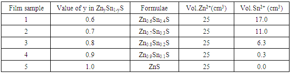
- Optical effects deal with transitions between bands and or energy levels inside the band gap. Thus optical measurements are of importance to analyze semiconductors. Figure 1 shows spectra transmittance of transmittance of ZnySn1-yS thin films.
 | Figure 1. A graph of transmittance (%) against wavelength (nm) |
 | Figure 2. Optimized transmittance against doping levels of Sn |
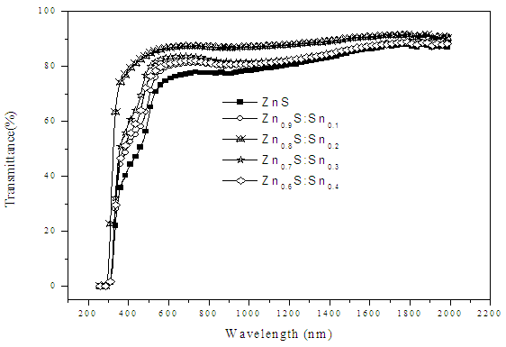
 | Figure 3. Transmission simulated curves for Zn0.8S:Sn0.2 thin films |
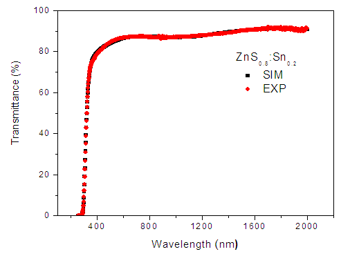
 | Figure 4. A graph of Reflectance (%) against wavelength (nm) |
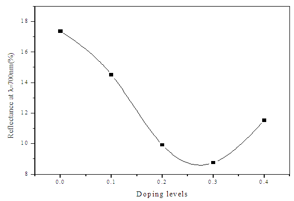 | Figure 5. Optimized Reflectance with doping levels of Sn |
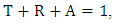 | (1) |
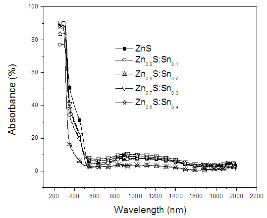 | Figure 6. A graph of absorbance (%) against wavelength (nm) |
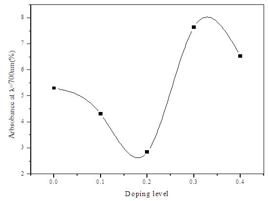 | Figure 7. Absorbance with doping levels of Sn at λ= 700nm |
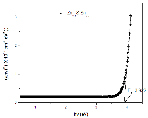 | Figure 8. Graphical determination of band gap of Zn0.8Sn0.2S thin film |
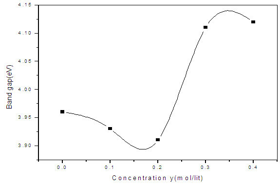 | Figure 9. The plot of band gap energy (eV) of ZnS:Sn thin films versus doping concentrations y |
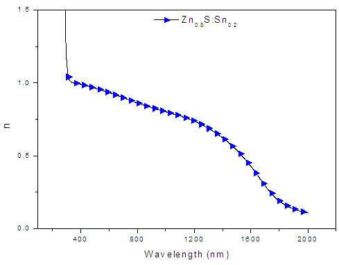 | Figure 10. A graph of refractive index (n) against wavelength (nm) for Zn0.8Sn0.2S films |
3.2. Electrical Properties of ZnS:Sn Thin Films
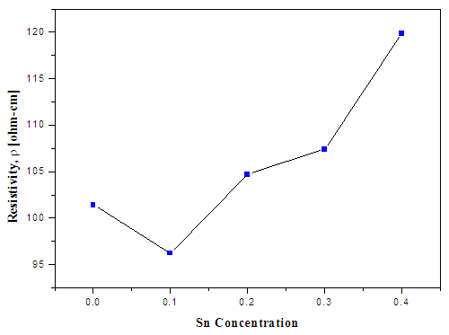
- The sheet resistivity of ZnS:Sn films was measured by using the four point probe. From figure 11 it is observed that resistivity increased with increase in Sn ion concentration and it ranged between, 9.62 × 101 Ω-cm to 1.19 × 10² Ω-cm.
 | Figure 11. Sheet resistivity against Sn concentration in ZnS:Sn films |
4. Conclusions
- ZnS:Sn films were successfully deposited on glass substrate by chemical bath deposition technique at 80°C. Electrical and optical properties of the deposited thin films have been found to be significantly dependent on Sn concentration during deposition. From optimized data, Zn0.8S:Sn0.2 films had high transmittance of 87% at λ=700nm and corresponding reflectance of 10%. The band gap obtained ranged from 3.91eV to 4.12 eV with Zn0.8S:Sn0.2 films having band gap energy of 3.92eV. Refractive index and dielectric constants decreased with increase in Sn concentration indicating an increase in transparency. Their resistivity increased with increase in zinc concentrations and it ranged from 1.01 × 10² Ω-cm to 1.20 × 10²Ω-cm. This was attributed to the introduction of tin into the molecular interspacing in ZnS crystals. Pure ZnS films had a resistivity of 1.01 × 10² Ω-cm. We recommend some work to be done on effect of Sn on structural properties of Zn0.8S:Sn0.2 films.
ACKNOWLEDGEMENTS
- The authors are grateful to the assistance offered by the Physics Department of Kenyatta University where this study was carried out. They also acknowledge the University of Nairobi department of Physics [Chiromo Campus] for kindly providing the UV-VIS-NIR spectrophotometer 3700 for the spectral analysis of the deposited thin films.