N. E. Makori, I. A. Amatalo, P. M. Karimi, W. K. Njoroge
Department of Physics, Kenyatta University, Nairobi, Kenya
Correspondence to: N. E. Makori, Department of Physics, Kenyatta University, Nairobi, Kenya.
| Email: |  |
Copyright © 2015 Scientific & Academic Publishing. All Rights Reserved.
Abstract
Solar energy has a great potential of meeting a large fraction of energy needs using photovoltaics. While most photovoltaic cells in use today are Silicon-based, cells of other semiconductor materials have been manufactured. Considerable research has been focused in search of thin-film photovoltaic cells with high conversion efficiency. In our early studies, we reported optimization of Tin Selenide (SnSe) and Tin doped Cadmium Oxide (CdO:Sn) thin films for solar cell applications. SnSe and CdO:Sn thin films were successfully deposited by thermal and reactive thermal evaporation respectively using Edward’s Auto 306 Magnetron Sputtering System. Their optical and electrical properties were studied using Solid Spec-3700 DUV Spectrophotometer and Four-Point-Probe respectively. Transmittance of SnSe thin films deposited had transmittance ranging 0.01% to 45% while the band gap values obtained were in the range of 1.71eV to 1.76eV. SnSe thin films showed decrease of resistivity from 181Ωcm to120Ωcm with increase in film thickness from 112nm to 148nm. The optical properties of CdO:Sn showed high transparency in the visible region which varied with Sn doping. CdO and CdO:Sn had a transmittance of 70% to 85% and 50% to 89% respectively within the visible range of the electromagnetic spectrum. Band gap energy for undoped CdO was 2.43eV while that of tin doped CdO was in the range of 3.19eV to 3.29eV for tin doping of 1% to 7%. Resistivity of CdO was 42Ωcm while that of tin doped CdO ranged between 16Ωcm to 93Ωcm. In this study, the optimized thin films were used to fabricate SnSe-CdO:Sn P-N junction. SnSe of film thickness 148nm and 3% Sn doped CdO were used in the fabrication of the junction whose parameters are; Isc = 0.993mA, Voc = 273mV, Imax = 0.905mA, Vmax = 207mV, FF = 0.69 and η = 0.59%.
Keywords:
Thermal evaporation, Thin film thickness, Tin doping, Optical properties, Electrical properties, I-V characteristics
Cite this paper: N. E. Makori, I. A. Amatalo, P. M. Karimi, W. K. Njoroge, Characterization of SnSe-CdO:Sn P-N Junction for Solar Cell Applications, International Journal of Energy Engineering, Vol. 5 No. 1, 2015, pp. 1-4. doi: 10.5923/j.ijee.20150501.01.
1. Introduction
Energy crisis due to a decline in fossil fuel stocks and increasing carbon dioxide emissions that are causing global warming has enhanced interest in the development of clean renewable sources of energy. The by-products of fossil fuels such as Carbon Dioxide, Sulphur and Nitrogen Oxide may result in acid rain. Hence it is important to switch for an energy source which is clean, efficient and in a sustainable form. To sustain human development, more electrical energy consumption is expected in future [1]. The solar cell industry is predominantly using Silicon based solar cell technology. Because of its indirect band gap silicon is not able to absorb much sunlight as compared to direct band gap materials [2]. Recently, the search for thin-film materials for solar energy conversion and other related applications has been intensified with SnSe as one of the materials. A Lot of effort has been geared towards metal chalcogenides as they have shown superior performance as compared to others [3]. Metal chalcogenides have been prepared in form of thin films by various researchers. For large scale production of solar cells, a thin film deposition technique that can be easily handled at low cost is needed [4].Tin Selenide is a narrow band gap binary IV-VI semiconductor material. It is thus capable of absorbing a major portion of solar energy hence its use in fabricating solar cells. It is also suitable for various optoelectronic applications like memory switching devices, light emitting devices (LED), holographic recording systems among others [5]. Tin based solar cells exhibit good optical properties and its alloys have high efficiency solar cell materials [6].Cadmium Oxide is an important n-type semiconductor material for the development of various technologies of solid-state devices. The semiconducting thin films of Cadmium Oxide are transparent in visible and NIR spectral regions [7]. Cadmium Oxide thin films find wide applications in the field of optoelectronic devices such as solar cells, phototransistors, photo-diodes and transparent electrodes [8]. Doping of CdO influences it optical and electrical properties. Tin doped CdO thin films prepared by [9] using electron beam technique reported that the films exhibited direct band-to-band transitions, which corresponded to optical band gaps of 3.1eV to 3.3eV with a transmittance value of ~83% and a resistivity value of 4.4 x 10⁻⁴Ωcm were achieved for (CdO)0.88(SnO2)0.12 film annealed at 350℃ for 15 minutes, whereas the maximum value of transmittance ~93% and a resistivity value of 2.4 x 10⁻³Ωcm were obtained at 350℃ for 30 minutes. These studies indicated that the optical and electrical properties of tin doped cadmium oxide varied with deposition parameters. The thin films are highly transparent in the visible region of electromagnetic spectrum therefore, appropriate for use as window layers in photovoltaic applications. p-type and n-type regions of different materials form a heterojunction [10]. In thin film solar cell fabrications, the use of a heterojunction with a large band gap window material and a small band gap absorber material is a means to minimize the surface recombination loss that might otherwise dominate in direct band gap materials. In thin film solar cells, a junction occurs between the absorber layer and the window layer. The window layer allows the light to pass through it and travel to the absorber layer creating electron hole pairs thereby supplying current to an external load.Thin film solar cells are usually produced by physical or chemical deposition techniques. Thin film technology is of much commercial interests because it offers lower costs and possibilities for mass production [11]. In the thin film approach, reduction of cost is achieved by using small amount of material and inexpensive processing. Thin-film technologies are developed as a means of substantially reducing the cost of photovoltaic systems. In our early studies, thin film thickness of SnSe and Sn doping of CdO were the major parameters optimized for SnSe-CdO:Sn fabrication.
2. Experimental Procedure
Tin and Selenium elements were mixed in a ratio of 1:1 and heated in a glass tube until they melted to form a homogeneous alloy. The alloy was allowed to cool in sealed glass tubes to prevent oxidation of Tin and Selenium. Clean glass substrates were then mounted on a substrate holder of the Edwards Auto 306 Magnetron Sputtering System. 1.20g of the alloy was placed on a boat and then the chamber covered tightly and chamber evacuated. Deposition parameters are shown in table 1. Film thickness of SnSe samples was determined using a Profilometer. | Table 1. Deposition parameters of SnSe thin films |
| | Parameter | Units | | Deposition Temperature | 448 K | | Base Pressure | 3.2 x 10⁻⁵ mbars | | Heater Current | 3.2 A | | Substrate to Boat Distance | 15.0 cm | | Deposition Time | 1 Minute |
|
|
To prepare CdO:Sn thin films, Cadmium and Tin were mixed at a predetermined ratio (3% of Sn in CdO). Cadmium and Tin were heated in glass tubes until they melted while shaking to form a homogeneous alloy. They were allowed to cool in sealed glass tubes to prevent oxidation of Cadmium and Tin. Clean glass substrates were then mounted on a substrate holder of the Edwards Auto 306 Magnetron Sputtering System. About 1g of Cadmium and Tin alloy were placed on a boat and then the chamber covered tightly, evacuated and the alloy heated in the presence of Oxygen. The deposition parameters are shown in table 2. | Table 2. Deposition parameters of CdO:Sn thin films |
| | Parameter | Units | | Oxygen Flow rate | 20 sccm | | Deposition Temperature | 453 K | | Base Pressure | 3.8 x 10⁻⁵mbars | | Heater Current | 3.0 A | | Heater to Boat Distance | 15.0 cm | | Deposition Time | 1 Minute |
|
|
Sheet resistance measurements of SnSe and CdO:Sn were done using Four Point Probe method. Sheet resistance measurements were done at room temperature and pressure. Fabrication of SnSe-CdO:Sn P-N junction solar cell, glass Ag/CdO:Sn/SnSe/Ag was done in stages in the Edwards Magnetron Sputtering System. First, the n-type 3% Sn doped CdO thin film was deposited onto a glass substrate (whose one end had Silver paste) by reactive thermal evaporation method. Secondly, the p-type 148nm SnSe thin film were deposited onto CdO:Sn on the same substrate to form a second layer. Fabrication of the solar cell was completed by depositing Silver (Ag) back contact on one end of SnSe. The schematic diagram of the fabricated solar cell is as shown in figure 1. | Figure 1. Schematic diagram of SnSe-CdO:Sn P-N junction solar cell |
Incident Photon Conversion Efficiency apparatus was used to obtain I-V characteristics.
3. Results and Discussions
3.1. Optical Properties of SnSe and CdO:Sn
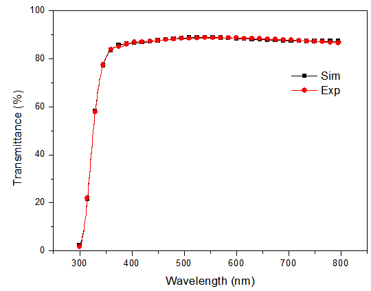
The experimental and simulated graphs of SnSe of film thickness 148nm and 3% Sn doped CdO transmittance is shown in figure 2 and 3 respectively.SnSe had a transmittance1% to 36% for incident photons of wavelengths of 300nm to 1000 nm. The low transmittance implies high absorption of SnSe thin films. While CdO:Sn had an optical transparency ranging from 60% to 89% within the visible region of electromagnetic spectrum.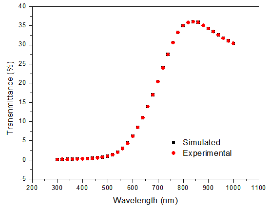 | Figure 2. Experimental and simulated graph of SnSe |
 | Figure 3. Experimental and simulated graph of CdO:Sn |
Energy band gaps of SnSe thin films were extracted from the simulated transmittance data of SCOUT 2.4 software. The band-gap energy and the transition type can also be derived from the mathematical treatment of the data obtained from the optical absorbance vs. wavelength using equation (1).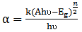 | (1) |
Straight line plots of  as a function of
  : an extrapolation of the value of
  to zero, also give
  . If a straight line for n=1, is obtained then, there is a direct electron transition between the states of the semiconductor, whereas for n=4, the electron transition is indirect.It is assumed that the absorption coefficient (α), in equation (1) near the band edge shows an exponential dependence on photon energy for many materials [12]. This dependence is given as follows in equation (2).
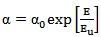 | (2) |
Where, αo, is a constant and Eu is Urbach energy which is the width of the tail of the localized state associated with the amorphous state in the forbidden band.The band gap values of SnSe and CdO:Sn obtained were 1.71eV and 3.19eV respectively.
3.2. Electrical Resistivity of SnSe and CdO:Sn
The sheet resistance measurements obtained were used to calculate resistivity of SnSe and CdO:Sn thin films using equation (3). , In typical usage the current is set to 4.53 mA so that the resistivity is simply the voltage reading in mV. Table 3 shows the sheet resistance and electrical resistivity of SnSn and 3% Sn doped CdO.
 | Table 3. Sheet resistance and resistivity of SnSe and 3% CdO:Sn |
| | Semi-conductor | Sheet resistance x 105 ± 500 Ω/□ | Resistivity x 101 (Ωcm) | | SnSe | 17.9 | 12.0 | | CdO:Sn | 2.78 | 1.8 |
|
|
In our early studies, we reported that low electrical resistivity measurements of 148nm SnSe and 3% Sn doped CdO made them suitable for fabricating SnSe-CdO:Sn PN-junction. Moreover, low transmittance and high absorption coefficient are the parameters needed for an absorber layer for photovoltaic applications, while high transmittance and low absorption are some of the optical properties which are considered when choosing a window layer.
4. I-V characteristics of SnSe-CdO:Sn pn-Junction
Open circuit voltage (Voc), maximum output voltage (Vmax), short circuit current (Isc) and maximum output current (Imax), the fill factor (FF) and conversion efficiency (η) parameters of SnSe-CdO:Sn pn-junction obtained are given in table 4.| Table 4. Parameters of SnSe-CdO:Sn PN-junction |
| | PARAMETER | VALUE | | Voc | 273 mV | | Vmax | 207 mV | | Isc | 0.993 mA | | Imax | 0.905 mA | | Fill factor (FF) | 0.69 | | Efficiency (η) | 0.59% |
|
|
Cell energy conversion efficiency (η), was calculated using equation (4).  | (4) |
Where E is the light irradiance (in W/m2), A is the surface area of the solar cell (in m2) and Pmax= VmaxImax.The fill factor, FF was calculated using equation (5). | (5) |
The I-V characteristics obtained are shown in figure 4.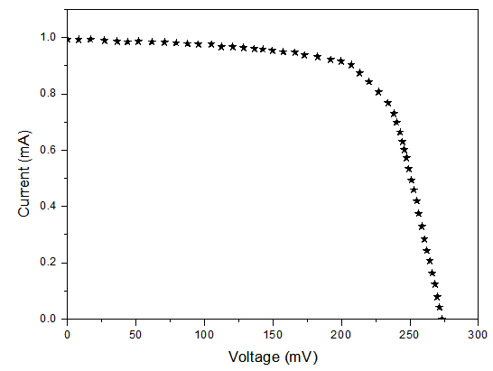 | Figure 4. I-V Characteristics of SnSe-CdO:Sn PN-junction |
Tin doped Cadmium Oxide prepared by [13] and used as a window layer resulted to a conversion efficiency of 14.3% in CdTe/CdS. In this study CdO:Sn was used as a single window layer in fabricating a solar cell with SnSe as an absorber layer.
5. Conclusions
Tin Selenide and 3% Sn doped CdO thin films were successfully deposited on glass substrate using thermal evaporation. SnSe and CdO:Sn thin films were used to fabricate SnSe-CdO:Sn P-N junction. The I-V characteristics obtained indicates that SnSe and tin doped CdO used in fabricating SnSe-CdO:Sn P-N junction are potential materials for photovoltaic applications.The following are recommended for further study geared towards improving the conversion efficiency of the fabricated glass/Ag/CdO:Sn/SnSe/Ag solar cell. I-V characteristics of various SnSe-CdO:Sn PN- junctions fabricated using SnSe thin films deposited at different temperatures be investigated. Secondly, multilayered photovoltaic cell using SnSe and CdO:Sn should be studied. Moreover, the effect of using different ohmic contacts other than Silver on SnSe-CdO:Sn P-N junction should be investigated to find out the ones which give the highest conversion efficiency.
ACKNOWLEDGEMENTS
We express our gratefulness to the members of the Physics Department for their moral support. We also extend our heartfelt thanks to the laboratory technicians of Physics Department Kenyatta and Nairobi Universities for their technical input. Finally, we thank the Kenyatta University administration for providing conducive learning environment.
References
| [1] | Kuo-Jui H., 2010. Electron-Reflector strategy for CdTe thin-film solar cells. PhD Thesis. Colorado State University, Department of Physics, USA. |
| [2] | Fahrenbruch A. L. and Bube R .H. 1983. Fundamentals of Solar cells. New York Academic Press, USA. |
| [3] | Lindgren T., Larsson M. and Lindquist S., 2002. Solar Energy Materials. Journal of Solar cells, 73, 377-377. |
| [4] | Mariappan R., Ragavenda M. and Gowrisankar G., 2010. Growth and characterization of SnSe thin films prepared by spray pyrolysis technique. Chalcogenide Letters, 7, 211- 216. |
| [5] | Kumar, N., 2012. Effect of Film Thickness on Optical Properties of Tin Selenide Thin Films Prepared by Thermal Evaporation for Photovoltaic Applications. American Journal of Materials Science, 2, 41-45. |
| [6] | Toshiyuki Y., Jiro M. and Akira Y., 1991. Thin films of CuInSe2 prepared by RF sputtering from various compositional powder targets. Solar Energy Materials and Solar Cells, 27, 25-35. |
| [7] | Hamadi O.A., Shakir N.J. and Mohammed F.H., 2010. Magnetic Field and Temperature Dependent Measurements of Hall Coefficient in Thermal Evaporated Tin-Doped Cadmium Oxide Thin Films. Physics Journal, 37, 223–231. |
| [8] | Gowri S., 2003. Characterization of Cadmium Zinc Telluride Solar Cells. Msc Thesis. University of South Florida, College of Engineering: Department of Electrical Engineering. USA. |
| [9] | Ali H. M., Mohamedy H. A., Wakkad M. M., and Hasaneen M. F., 2009. Optical and Electrical Properties of Tin-Doped Cadmium Oxide Films Prepared by Electron Beam Technique. Japanese Journal of Applied Physics, 48, 1-7. |
| [10] | Brennan K.F., 1999. The physics of semiconductors with applications to optoelectronic devices. Cambridge University Press, United Kingdom. |
| [11] | Zhou D., 2008. Light-trapping enhancement in thin film solar cells with photonic crystals. Msc Thesis. Iowa State University. Ames, Iowa. |
| [12] | Urbach F., 1953. The long-wavelength edge of photographic sensitivity and of the electronic absorption of solids. Physical Review, 92, 1324-1324. |
| [13] | Zhiyong Z., Komin V., Viswanathan V., Morel D.L., Ferekides C.S., 2000. Application of tin-doped Cadmium oxide films in CdTe/CdS solar cells. Photovoltaic Specialists Conference Report. |
 Abstract
 Reference
 Full-Text PDF
 Full-text HTML