-
Paper Information
- Previous Paper
- Paper Submission
-
Journal Information
- About This Journal
- Editorial Board
- Current Issue
- Archive
- Author Guidelines
- Contact Us
International Journal of Energy Engineering
p-ISSN: 2163-1891 e-ISSN: 2163-1905
2014; 4(3): 61-67
doi:10.5923/j.ijee.20140403.03
Investigation of the Properties of Cadmium Sulphide Thin Films for Solar Cell Applications
 Abstract
 Reference
 Full-Text PDF
 Full-text HTML
M. Abulmakarim1, I. A. Rufai1, A. O. Musa2
1Department of Mechanical Engineering, Bayero University, Kano, Nigeria
2Department of Physics, Bayero University, Kano, Nigeria
Correspondence to: M. Abulmakarim, Department of Mechanical Engineering, Bayero University, Kano, Nigeria.
| Email: |  |
Copyright © 2014 Scientific & Academic Publishing. All Rights Reserved.
The paper presents an investigation of the properties of Cadmium Sulphide (CdS) thin films and their suitability for use as solar cell material. Thin films of cadmium sulphide with thicknesses ranging from 0.8-3.26 µm were deposited on microscope glass slides using the chemical bath deposition method (CBD). The paper also presents some findings on how to optimize the chemical bath deposition technique to achieve improved quality of CdS thin films deposited on glass substrates. Some of the samples were annealed while others were left unannealed. All the samples were tested to investigate the physical, electrical and optical characteristics of the deposited thin films. The physical properties measured were the thickness and surface morphology of the samples. The electrical properties were the resistivity, conductivity type and charge carrier mobility while the optical property was the band gap energy. The resistivity of the samples was measured using the four point probe method while the band gap energy was measured using a UV/VIS spectrophotometer. The unannealed samples were found to have an average resistivity of 1.01217 ×10³ Ωcm and average band gap energy of 2.493 eV. The average charge carrier mobility of the unannealed samples was 2209.4 cm2v-1s-1 measured based on the Hall Effect principle. From the galvanometer deflection as measured against standard using the hot probe method was observed that CdS is an n-type semiconducting material. Comparing results obtained for both annealed and unannealed samples, it was observed that there is a decrease of 4.63% on resistivity and 0.72% on band gap energy of the annealed samples. The charge carrier mobility increased by 12.3% for the annealed samples as well. The quality of CdS thin film can be improved through annealing. This implies that the thin film developed in the current study could be used as a window layer for heterojunction solar cells of the types; Cadmium sulphide/ Cupper Indium Selenide (CdS/CuInSe2) or Cadmium Sulphide/ Cadmium Telluride (CdS/CdTe).
Keywords: Chemical Bath Deposition, Cadmium Sulphide,Band Gap Energy, Annealing
Cite this paper: M. Abulmakarim, I. A. Rufai, A. O. Musa, Investigation of the Properties of Cadmium Sulphide Thin Films for Solar Cell Applications, International Journal of Energy Engineering, Vol. 4 No. 3, 2014, pp. 61-67. doi: 10.5923/j.ijee.20140403.03.
Article Outline
1. Introduction
- The investigation of the fundamental properties of CdS thin films is of paramount importance in the understanding and development of modern CdS cells. For several decades, many researchers have been studying these properties to see how the quality of this layer can be improved for better performance when converted into a wide variety of diverse modern devices. Some of these devices may include high speed transistors, solar cells, solid state lightening, sensors, and information storing devices and so on (Ramirez and Espinoza, 2009). The fundamental properties studied and presented in this research are the physical, electrical and optical characteristics of the deposited CdS layer. The discovery of the photovoltaic effect (PV) started with the discovery of Selenium in 1817 by Bezeluis who was the first to prepare elemental silicon. The PV effect was first observed in 1839 by French physicist, Edmon Becquerel (Fred and Shirland, 1996; Reynolds et al. 1954; Fahrenbruch and Bube, 1983).This was followed by the discovery of photoconductivity in Selenium in 1873 by Willoughby Smith. This latter effect increased a flurry of activities which included the discovery of spectral sensitivity of Selenium photoconductors, the proposal of a light meter and the observation of the PV effect in a solid state Selenium structure by Adams and Day in 1876 (Fred and Shirland, 1996; Fahrenbruch and Bube, 1983). A major development in solar cell technology was evidenced in the1940’s and 1950’s when the “Czochralski method” was developed for producing highly pure crystalline silicon (Mursheda, 2004). In 1954, work at Bell Telephone laboratory resulted in an Si cell with 4% efficiency, which was later increased this to 6% and then to 11% efficiency. Also in 1954 Cadmium Sulphide (CdS) p-n junction was produced with an efficiency of 6% (Fred and Shirland, 1996). CdS has a direct band gap of 2.42 eV and usually has a wurzite hexagonal structure. CdS is an type semiconductor with resistivity ranging from10−3 to 108 Ωcm (Fahrenbruch and Bube, 1983).Wu et al. (2001), Enriquez and Mathew (2003) and Ramirez and Espinoza (2009) suggested the possibility of obtaining good quality thin films using CBD method.The growth process involved in the deposition of the CdS layer is important in optimizing the quality of the thin film. The deposition of CdS by CBD is usually based on the decomposition of thiourea in an ammonical alkaline solution containing a cadmium salt. The reaction can be represented by equation 1 (Sandoval and Rameirez, 2009).
 | (1) |
 | (2) |
2. Materials and Methods
2.1. Preparation of CdS
- The reagents used in the preparation of the cadmium sulphide (CdS) thin film in this study include: cadmium chloride (CdCl2) as cadmium precursor which slowly release the Cd++; Ammonia; Water; and Thiourea (S=(NH2) 2) as sulfur precursor, which releases Sˉ ion by means of an alkaline hydrolysis process as described by Ramirez and Espinoza (2009). Two solutions were prepared: Solution one consists of 0.12 mole of Cadmium (II) Chloride (CdCl2); 0.036 mole of Ammonium Chloride (NH4Cl); and 0.73 mole of Ammonium Hydroxide (NH4OH). Solution two consists of 0.17 mole of Thiourea (S=C(NH2)2); 0.036 mole of Ammonium Chloride (NH4Cl); and 0.73 mole of Ammonium Hydroxide (NH4OH). The mass of the reagents used are shown in Table 1. Both solutions were preheated in a water bath at a temperature of 65℃ for twenty minutes and then mixed together in a beaker. The glass slide would fit well in a 500 ml beaker; therefore, both solutions were prepared in a 250 ml beaker separately and then mixed together. The presence of OH- (pH = 10-12) causes thiourea hydrolysis and metallic hydroxide synthesis. In this research, a pH level of 11 was maintained.
|
2.2. Deposition Process
- The chemical bath deposition technique was used for the deposition of the CdS thin film. The chemical bath deposition is a technique used to obtain thin organic semiconductor films from most cations of transition metals and metalloids, with anions of group 16, and more often with sulphide and selenide (Ramirez and Espinoza, 2009). Chemical bath deposition technique is also known as solution growth, controlled precipitation, or simply a chemical deposition. Semiconductor films of 20 to 1000 nm can be deposited in this way. In the current study, chemical bath deposition method was chosen due to its simplicity and cost effectiveness. The equipment in which the film synthesis takes place is very simple and does not require the passage of electric current through the solution as in electrolysis (Wu et al. 2001). The deposition of CdS on glass using the CBD method depends on six important parameters which includes: molar concentration of the reagents, pH level of the solution prepared, the deposition temperature, the deposition time, the stirring rate and the complexant agent used for slowing down the reaction.The surface of the glass slides were cleaned using methylated spirit and then rinsed thoroughly with deionized water and allowed to dry. The slides were suspended into the mixture using clamps. A magnetic stirring rod was placed inside the mixture and the stirring rate was maintained at approximately 100 rpm. Two (2) sets of four (4) samples (labeled A-D) were prepared. The duration for samples A1 and A2 was 4 hours, that of samples B1 and B2 was 3 hours, samples C1 andC2 was 2 hours and that of samples D1 and D2 was 1 hour. One set was annealed at a temperature of 400°C for 20 minutes and the other set were left unannealed. Heat treatment was used to induce more long–lasting changes in film properties. If oxygen is absorbed on the surface and in the grain boundaries of a CdS film, it removes electrons from the conduction band of the CdS in order to become chemically bound, thus building up a depletion layer at the surface and at the grain boundaries.
2.3. Measurement of the Fundamental Characteristics of CdS Layer
- In order to assess the performance of CdS thin films for solar cell application, the physical, electrical and optical characteristics of the layer must be studied carefully. The physical characteristics to be measured include; thickness and the surface morphology while the electrical characteristics may include; conductivity type, charge carrier mobility and resistivity. Lastly, the optical characteristic to be measured is the band gap energy.
2.3.1. Thickness Measurement
- The thicknesses of the films were determined using the microbalance gravimetric method (Kasturi and Inderjeet, 1983). Equation 3 was used to determine the thickness of the depositions.
 | (3) |
 | (4) |
2.3.2. Structural and Surface Morphology
- The surface structure of the CdS film was studied using the Stereotype Eye Piece microscopic digital camera.
2.3.3. Conductivity Type Measurement Using the Hot- probe
- The hot–probe measurement technique is a common method for rapidly determining whether a semiconductor is n– or p–type. It was considered in the current research because it simultaneously provides additional information on the diffusion process (Kasturi, 1983). It consists of a hot-point probe, usually a soldering iron heated to red level, a cold– point probe and a centre- zero milliammeter.
2.3.4. Resistivity (ρ) Measurement Using the Four Point Probe
- The four point probe method was used to measure the resistivity of the CdS layer. A JADEL of model RM3000 current source was used to pass in the current and measure the voltage drop across the semiconductor. A known current was passed in through the outer two probes while the voltage drop was measured using the two inner probes. A graph of voltage against current was plotted to obtain the slope (V/I). Semi conductor resistivity ρ was then computed from the formula presented in equation 5 (Sze S. M., 1969).
 | (5) |
2.3.5. Measurement of Charge - Carrier Mobility (µ)
- It is the central parameter in characterizing electron and hole transport due to drift. The Hall Effect principle was used for the measurement of carrier mobility. The principle is based on the fact that an electro-motive force (e.m.f) is set up across a current carrying conductor (or semiconductor) when a magnetic field is applied normal to the direction of flow of current. The charge carrier mobility was calculated using equation 4 (Sze S. M., 1969).
 | (6) |
2.3.6. Band Gap Energy
- A JENWAY 6405 UV/VIS Spectrophotometer was used to measure the absorbance of the CdS layer between the ultraviolet and visible range. The absorption coefficient (α) was computed using the Beer Lambert’s formula (Islam and Podder, 2009) given by equation 7.
 | (7) |
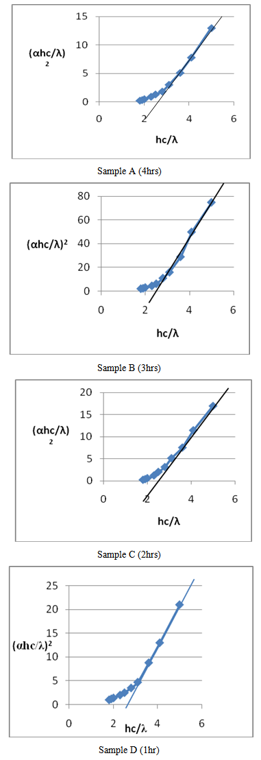
 against photon energy
  was plotted and a line tangential to the curve was drawn and extended until it touches the x-axis (photon energy). It should be noted here that: α - absorption coefficient; h - Planks constant, equals to 6.626 x 10⁻³⁴ Joules sec; C - Speed of light, equals to 3.0 x 10⁸ meter/sec; λ - Cut off wavelength; 1eV = 1.6 X 10⁻¹⁹ Joules (conversion factor). The point of intercept on the photon energy-axis determines the band gap energy.
 3. Results and Discussion
3.1. Results
3.1.1. Film Thickness
- Depositions with thicknesses of 3.2, 1.33, 0.9 and 0.8 µm were obtained for durations of 4, 3, 2, and 1 hour respectively. The results are presented in table 2.
3.1.2. Structure and Surface Morphology
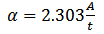
- A more homogenous deposition was observed in sample A followed by B, C and then D. Thus, the homogeneity, grain size and adhesion to the substrate can be increased by prolonging the deposition time and the volume of the solution (Figure 1).
 | Figure 1. Images of the CdS thin films |
3.1.3. Conductivity Type
- Films of CdS are n-type whether deposited by Vacuum Evaporation, Spray Pyrolisis or Chemical bath method (Fahrenbruch and Bube, 1983). The average value of voltages measured across the semiconductor was -0.285 V. The voltmeter reading was observed to be opposite in direction and of values -0.285 V when compared to that of p-type silicon which was observed to have a reading of +0.354 V.
3.1.4. Resistivity
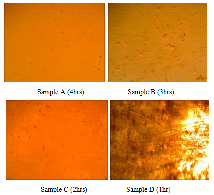
- The average value of resistivity for the annealed and unannealed samples in the current research was 9.653×10³ and 1.01217×10⁴ respectively. A decrease in average resistivity values of the samples were observed when the samples were annealed. This is in agreement with previous works in this field such as that of Chaure et al. (2003) and that of Sundus et al. (2013). The values obtained for sample A, B, C, and D are as presented in Table 2. Figure 2 presents the voltage-current characteristics for the 4 samples.
| |||||||||||||||||||||||||
 | Figure 2. Voltage against current for samples A, B, C and D |
3.1.5. Charge Carrier Mobility
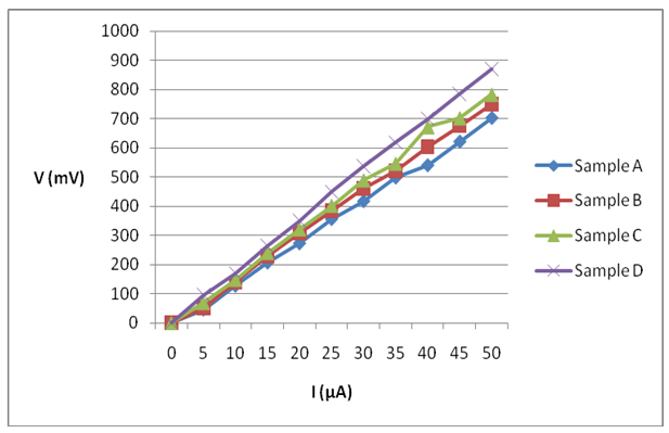
- The average charge carrier mobility for the annealed and unanannealed samples for this work was 2481.2 cm2v-1s-1 and 2209.4 cm2v-1s-1respectively. This is in agreement with results obtained by Chaure et al. (2003) and Sudus et al. (2013). The relationship between Hall voltages and the load voltages for the four samples is determined in Figure 3.
 | Figure 3. Graph of Hall voltage against load voltage for the samples |
3.1.6. Band Gap Energy
- The average band gap energy measured for the annealed and unannealed samples in this research were 2.475 eV and 2.493 eV respectively, which are in agreement with similar findings reported in the literature (Chaure et al., 2003; (Dipalee et al., 2011; Kathirvel et al., 2011; Jadhav et al., 2014). Upon annealing, a shift from 2.42 to 2.25 eV, 2.45 to 2.42 eV, 2.10 to 2.40 eV and 2.4 eV was observed by these researchers respectively.A linear relationship was observed at the upper sections of the plots for both annealed and unannealed samples (Figure 4 A, B, C and D.). This indicates that the CdS thin film is a direct band gap material. CdS has direct band gap at room temperature with high optical transition probabilities for absorption and emission as described by Khomane, (2011). Explorations were drawn from the upper straight portions of the graph to cut through the Eg-axis to obtain the band gap of the material.
 | Figure 4. Band gap energy for the samples |
3.2. Discussion
- Under ideal conditions, the reaction between the reagents used in the production of the CdS thin film results in a homogenous deposition that is well adhered to the substrate (Ramirez and Espinoza, 2009). However, during the experiments reported in the current study, it was observed that that the reaction was occurring too fast and no homogenous formation of CdS thin films on the substrate. This was clearly noticed as the solution rapidly changed from colorless to light green, from light green to yellow and finally to deep orange color.In an attempt to find a solution to this problem, six different parameters (the molar concentration of the reagents, deposition temperature, deposition time, stirring rate and temperature of the mixture and the complexant agent used) were varied and the experiment repeated to allow for the gradual deposition of CdS on the substrate. The complexant agent used in this research was ammonia, which controled the alkalinity of the solution, thereby slowing down the velocity of the reaction.Ramirez and Espinoza (2099) reported the possibility of achieving thicknesses ranging from 20 to 1000 nm using the CBD method. In the current research, thicknesses ranging from 0.8 to 3.26 µm were achieved using the CBD method. This may be as a result of longer hours of deposition ranging from 1 to 4 hours. Resistivity ranging from 10-2 to 108 Ωcm can be achieved for CdS thin films deposited on amorphous substrates (Fahrenbruch abd Bube, 1983; Chaure et al., 2003; Sundus et al., 2013). In the current research, resistivity of 9.653×10³ Ωcm and 1.101217×10⁴ Ωcm were achieved for annealed and unannealed samples. To achieve the maximum electrical power conversion efficiency, there is need to have a semi conductor material with a low resistivity. Low resistivity also allows effective separation of electrons and holes. The charge carrier mobility for CdS thin films ranged between 1 and 105 cm2V-1s-1 (Fahrenbruch and Bube, 1983). The results obtained in the current research were 2481.2 cm2v-1s-1 and 2209.4 cm2v-1s-1 respectively. This is in agreement with results obtained by Chaure et al. (2003) and Sudus et al. (2013). It was also observed that with increase in thickness, there was a corresponding increase in the charge carrier mobility of the material. The charge carrier mobility was, also, found to be inversely proportional to the roughness. In order for an electron to jump from a valence band to a conduction band, it requires a specific minimum amount of energy for the transition called “the band gap energy”. The average band gap energy in obtained in the experiments reported in this paper were 2.475 and 2.593 eV for the annealed and unannealed samples respectively. It should be noted that the band gap energy of insulators is large (> 4 eV), but lower for semiconductors (< 3 eV) as reported by Metha (2000).
4. Conclusions
- The fundamental properties of CdS thin films, prepared using CBD method, were investigated. The properties studied include thickness, resistivity, charge carrier mobility, and band gap energy of the CdS layer. The thicknesses were determined using the density- mass relationship, which ranged between 0.8 µm and 3.2 µm. It was found out that there were better results in terms of resistivity, band gap energy and charge carrier mobility as thickness increased. The resistivity of the samples was investigated using the four point collinear probe method and an average resistivity of 9.653×10³ Ωcm was obtained. This value is within a reasonable range and in agreement with the results of previous findings reported in the literature (Fahrenbruch and Bube, 1983; Chaure et al., 2003; Sundus et al., 2013). Analysis of the results from the current research indicated that the CdS thin film developed is an n-type semiconducting material. The Hall Effect principle was used for the measurement of carrier mobility. The average charge carrier mobility for the annealed and unanannealed samples were 2481.2 cm2V-1s-1 and 2209.4 cm2V-1s-1 respectively. This indicates that the samples exhibited better results after annealing. The charge carrier mobility is within the acceptable range. The average band gap energy measured for the annealed and unannealed samples in the current research were 2.475 eV and 2.493 eV respectively which is in agreement with similar findings reported in the literature. UV/VIS Spectrophotometer was used to measure the absorbance of the CdS layer between the ultraviolet and visible range. Upon annealing, improvements were observed in terms of average resistivity which decreased by 4.63%, charge carrier mobility increased by 12.3% whiles the band gap energy reduced by 0.72%. Guided by theoretical and experimental findings, the fundamental properties of the deposited CdS layer have presented values within the required range. Based on findings of the current research and reports of similar works described in the literature, it can be concluded that the developed CdS thin film would have high potentials for solar cell applications.
Nomenclature
- ρ is the density of CdS v is the volumea is the area t is the film thicknessM is the mass of the depositionMT is the mass of both slide and depositionME is the mass of empty slide S = probe spacing V = voltage I = the currentW= width of the slide L= Length of the slide B=magnetic force (Tesla)A= absorbanceα= absorption coefficient h = Planks constant = 6.626 x 10⁻³⁴ Joules sec; C = Speed of light = 3.0 x 10⁸ meter/sec; λ = Cut off wavelength; 1eV = 1.6 X 10⁻¹⁹ Joules (conversion factor)