-
Paper Information
- Next Paper
- Previous Paper
- Paper Submission
-
Journal Information
- About This Journal
- Editorial Board
- Current Issue
- Archive
- Author Guidelines
- Contact Us
International Journal of Energy Engineering
p-ISSN: 2163-1891 e-ISSN: 2163-1905
2013; 3(3): 183-189
doi:10.5923/j.ijee.20130303.09
Effect of Recombination on Series Resistance in eta Solar Cell Modified with In(OH)xSy Buffer Layer
 Abstract
 Reference
 Full-Text PDF
 Full-text HTML
Robinson Musembi1, Bernard Aduda1, Julius Mwabora1, Marin Rusu2, Konstantinos Fostiropoulos2, Martha Lux-Steiner2
1Department of Physics, University of Nairobi, Nairobi, P.O. Box 30197-00100, Kenya
2Helmholtz-Zentrum Berlin fur Materialen und Energie, Lise Meitner Campus, Glienicker Strasse 100, 14109, Berlin Germany
Correspondence to: Robinson Musembi, Department of Physics, University of Nairobi, Nairobi, P.O. Box 30197-00100, Kenya.
| Email: |  |
Copyright © 2012 Scientific & Academic Publishing. All Rights Reserved.
Transport mechanism studies in TiO2/In(OH)xSy/Pb(OH)xSy/PEDOT:PSS eta solar cell have been carried out. The characterizations have been performed both in the dark and under varying illumination intensity for temperature range 200 K – 320 K. Calculations from ideality factor have shown that the recombination process of the eta solar cell in the dark to be tunneling enhanced, while under illumination it is thermally activated and takes place through exponentially distributed energy recombination levels. The temperature has been found to influence series resistance of the solar cell. Series resistance has been found to be high at low temperature and low at higher temperature, thus we can conclude that the recombination is thermally activated.
Keywords: Eta Solar Cell, Recombination, Series Resistance, Buffer Layer
Cite this paper: Robinson Musembi, Bernard Aduda, Julius Mwabora, Marin Rusu, Konstantinos Fostiropoulos, Martha Lux-Steiner, Effect of Recombination on Series Resistance in eta Solar Cell Modified with In(OH)xSy Buffer Layer, International Journal of Energy Engineering, Vol. 3 No. 3, 2013, pp. 183-189. doi: 10.5923/j.ijee.20130303.09.
Article Outline
1. Introduction
- The eta solar cell is based on a new concept proposed a few years ago by Prof. Könenkamp group[1, 2] and is based on the concept of two types of solar cells: the dye sensitized solar cell model (nanostructured configuration, separation of light absorption from charge transport, and majority carrier type of device) and classical solar cells idea (all solid state, use of inorganic materials)[1, 2, 3, 4]. Dye sensitized solar cell is a majority carrier type of device made up of mainly nanoporous TiO2 thin film which is covered with dye monolayer and then a liquid electrolyte is applied, the front electrode is provided by the SnO2:F glass substrate while the counter electrode is made from platinum coated glass[5]. On the other hand, the eta solar cell instead of having a monolayer of dye molecule, an extremely thin absorber (eta) material is sandwiched between two wide band gap n- and p- type materials. The eta solar cell is thus a combination of dye sensitized and classical solar cell concepts[6].A number of devices based on eta concept have been reported with mainly the extremely thin absorber material of choice being CdTe[7], a-Si[8], CuInS2[9], and PbS/ Pb(OH)xSy[10, 11]. Nonetheless, the knowledge about the effect of recombination mechanism on the series resistance in eta solar cell is still limited. In this article, we report on this subject through characterization of temperature dependence of J-V curves of an highly structured TiO2/ In(OH)xSy/Pb(OH)xSy/PEDOT:PSS/Au solar cell at different illumination intensities.
2. Experimental Method
- The solar cells based on Pb(OH)xSy eta material were fabricated by the following method: the substrate used was a 15 Ω/sq sheet resistance SnO2: F glass from Förschungszentrum Jülich. The substrate window layer used for our solar cell was 2 µm thick TiO2 thin films deposited by sol-gel technique at SgLux GmbH. The other thin film layers coated were 80 nm thick indium hydroxyl sulphide, In(OH)xSy, and approximately 10 nm thick lead hydroxyl sulphide, Pb(OH)xSy, successively by chemical bath deposition method using the following precursors: an aqueous solution containing 0.025 M InCl3, 0.1 M thioacetamide, and 0.005 M HCl was deposited at 70℃ , and the procedure was repeated three times by preparing fresh chemical bath after every 30 minutes, following a similar procedure as described elsewhere[6, 7, 11] and clearly illustrated in figure 1. Likewise, Pb(OH)xSy was deposited from an aqueous solution containing 0.05 M Pb(CH3OOH)2, 0.2 M NaOH, 0.05M triethanolamine, and 0.05 M thiourea at 40℃ for 10 minutes. The last thin film layer to be deposited was an electrically conducting polymer material poly(3,4- ethylenedioxythiophene) (PEDOT) doped with water soluble polyelectrolyte known as polystyrene sulfonate acid (PSS), was deposited undiluted by spin coating technique.
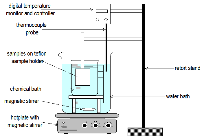 | Figure 1. setup for chemical bath deposition used in depositing In(OH)xSy and Pb(OH)xSy, respectively |
3. Transport Mechanism Theory
- The one diode model developed for polycrystalline heteronjunction thin film solar cell was used for describing and analyzing the JV - T curves of the eta solar cell in the dark and under illumination[12, 13]. The forward current density J of the heterojunction is described by
 | (1) |
 are the ideality factor, saturation current density of the diode and the thermal voltage, respectively. The term
  is the temperature dependent prefactor, while
  is the activation energy of the recombination. Equation 1 can be rearranged to give approximation of open circuit voltage as[12, 13]
 | (2) |
 is the short circuit current density. In equation 2, if we assume
  are independent of
  , a plot of
  as a function of
  should yield a straight line and the extrapolation to
  gives the activation energy
  . However when tunneling process is significant, equation 2 can be reorganized to give[12, 13]
 | (3) |
 as a function of the inverse temperature
  will yield a straight line with a slope giving us a precise value of activation energy
  . The value of activation energy can guide us in deducing the type of recombination process taking place in a solar cell device: when
  (where
  is the band gap energy) will indicate that recombination is taking place in the bulk of the materials absorber, or interface recombination is dominant when
 [12, 13].
4. Results and Discussion
- The solar cell structure based on the novel eta concept studied in this work is shown in figure 2.The extremely thin absorber material made of Pb(OH)xSy is sandwiched between two large bandgap materials, one n-type (TiO2) and the other p-type (PEDOT:PSS), the bandgaps of the two semiconductors are 3.2 eV[10,11] and 2.0 eV[16], respectively. The solar cell is completed with Au back contact with front contact being provided by SnO2:F layer or a thin film of gold on the glass substrate. The graph shown in figure 3 is for a solar cell without a buffer layer, the J-V curve under illumination is almost ohmic, showing that there is a lot of interface recombination taking place between TiO2/Pb(OH)xSy, the conversion efficiency is observed to be around 0.01%, consequently there is a need for a buffer layer of a material compatible with TiO2 and Pb(OH)xSy in order to mitigate the loss of charge carriers.The material chosen for this purpose is In(OH)xSy, its suitability as a buffer layer is well described in the literature[16,17]. The as prepared solar cell after inserting the buffer layer, the current density-voltage characteristics do not display a good conversion efficiency, this is as shown in figure 4 where an efficiency of 0.07% was realized, The other solar cell parameters were current density 0.7 mA/cm2, open circuit voltage Voc = 308 mV and fill factor of 0.3021.After annealing the buffer layer at 300℃ for 30 minutes, the solar cell shows tremendous improvement in terms of the overall conversion efficiency. The changes observed in the conversion efficiency of the solar cell after annealing can be attributed to two changes which occur in the buffer layer: the material changes from amorphous state to crystalline state and also becomes slightly rich in In2S3 content, this is well described in the literature by Bayon, et. al.,[18,19] and Kumaresan et. al.,[20]. The solar cell which demonstrated the best efficiency after annealing the buffer layer was chosen for transport mechanism studies.The solar cell analyzed for current generation and recombination properties had a structure of the type TiO2/In(OH)xSy/Pb(OH)xSy/PEDOT:PSS/Au eta solar cell, which under AM 1.5 conditions had the following parameters: open circuit voltage Voc = 0.249 V, short circuit current density Jsc = 9.24 mA/cm2, fill factor of 0.34, and finally the overall conversion efficiency of 0.78%.The current density – voltage data for the TiO2/ In(OH)xSy/Pb(OH)xSy/PEDOT: PSS/Au eta solar cells was measured as a function of temperature from 200 K to 320 K, and at different light intensities, thereafter valuable data was then extracted for further analysis.Figure 5 shows the temperature dependency of conversion efficiency of the In(OH)xSy modified eta solar cell. The conversion efficiency is observed to vary inversely with temperature at different illumination intensities. The results shows that temperature and illumination intensity have strong influence on the conversion efficiency of the eta solar cell with the highest values being observed at low temperature of 200 K, the conversion efficiency is observed to be increasing from 0.54% to 0.85%.Using models described in section 3 and in further details as reported elsewhere[6,13], equation 2, can be used to fit open circuit voltage as a function of temperature to the plot of illumination intensity dependent
 versus
  and assuming that
  are independent of temperature, a linear extrapolation to
  gives an activation energy
  , this is shown in figure 6. According to work done by Bayon, et. al.,[10, 11], the activation energy value is close to the chemical bath deposited Pb(OH)xSy band gap,
  . From this analysis, it follows that
  indicating that recombination mechanism in this type of device takes place in the bulk of the absorber material, also, it can be deduced that the band gap of the chemical bath deposited Pb(OH)xSy can be engineered for further widening. These results corroborate earlier findings by Koenenkamp and Hoyer[13].
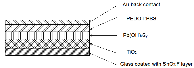 | Figure 2. The structure of the eta solar cell fabricated and studied in this work |
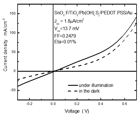 | Figure 3. The current density – voltage characteristics for the solar cell structure shown in figure 1 |
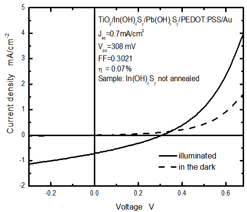 | Figure 4. The current density – voltage characteristics for the solar cell with a buffer layer of In(OH)xSy |
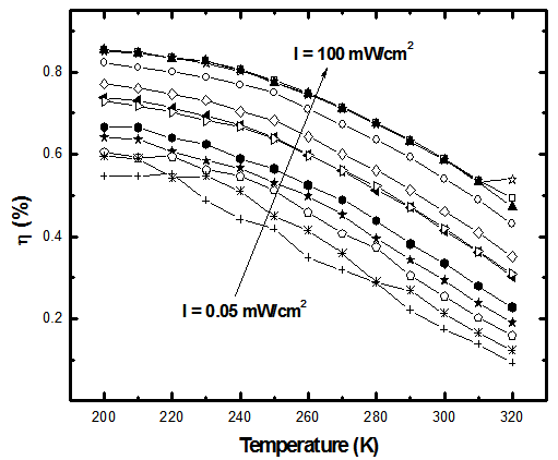 | Figure 5. temperature dependency of conversion efficiency at different illumination intensities I = 0.05 mW/cm2 – 100 mW/cm2 |
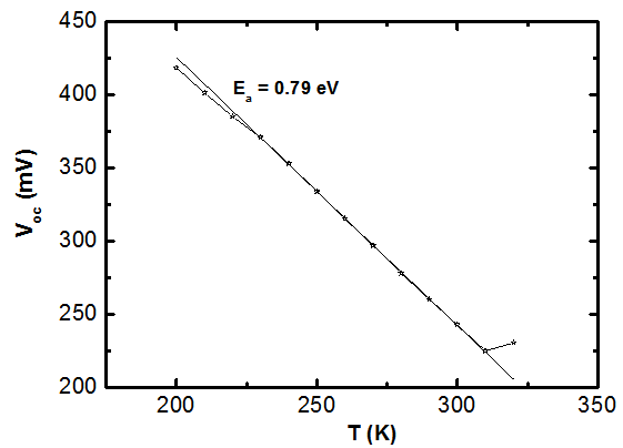 | Figure 6. activation enrgy of recombination derived from open circuit voltage Uoc as a function of temperature |
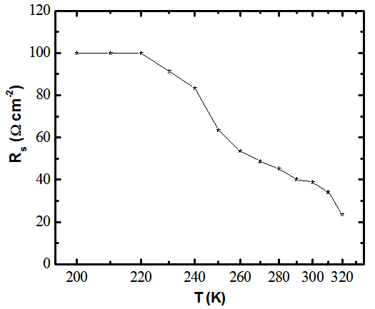 | Figure 7. Temperature dependence of series resistance of eta solar as extracted from temperature dependent current density-voltage data |
- Figure 7 shows temperature dependence of series resistance of the eta solar cell. The result shows that the eta solar cell had high resistance when it is operated at low temperature environment than when the temperature is raised to above the room temperature. The behaviour of the series resistance can be attributed to the number of available charge carriers in the solar cell. Since the series resistance is decreasing with temperature it can be deduced that recombination in the eta solar cell is thermally activated process at high temperature and tunneling assisted process at lower temperatures.The deduction from the series resistance behaviour is corroborated by similar work reported elsewhere[6,13]. Using equation 3, calculations show that the ideality factor of the eta solar cell is observed to decrease with increasing temperature. In the dark the ideality factor is given by
 , while under illumination it is given by
  . The temperature behaviour of the ideality factor in the dark indicates that recombination mechanism of eta solar cell is dominated by tunneling process while under illumination the charge carrier recombination is thermally activated since there is observed temperature dependence[6, 13]. It can also be deduced from the observation that ideality factor decreases as the temperature increases from 1.6 at
  to 1.2 at 320 K showing that recombination occurs through exponentially distributed energy recombination levels. The values of ideality factor at high temperature under illumination shows the recombination occurs through shallow levels, while at low temperatures deep levels are involved in the recombination as reported in literature[13].
5. Conclusions
- Operation temperature of the TiO2/In(OH)xSy/ Pb(OH)xSy/PEDOT: PSS solar cell has been found to strongly influence the conversion efficiency of the eta solar cell. Analysis of the ideality factor shows that recombination is tunneling enhanced dominated process when the solar cell is operated in the dark while under illumination it is thermally activated and takes place in the bulk of the absorber material at high temperatures, but at low temperature it takes place in the shallow levels. The parasitic series resistance has been observed to vary with temperature, it is highest at low temperature of around 200K and lowest when temperature is elevated to 320K, this shows that the recombination is a thermally activated process and strongly influences series resistance of the solar cell.
ACKNOWLEDGEMENTS
- RM would like to thank the group of Organic materials at Helmholtz-Zentrum for financial support, also thanked for financial support are IPPS Sweden and the University of Nairobi, Kenya.