-
Paper Information
- Next Paper
- Previous Paper
- Paper Submission
-
Journal Information
- About This Journal
- Editorial Board
- Current Issue
- Archive
- Author Guidelines
- Contact Us
International Journal of Energy Engineering
p-ISSN: 2163-1891 e-ISSN: 2163-1905
2013; 3(2): 97-109
doi:10.5923/j.ijee.20130302.06
Conversion Circuit Design for High Efficiency Bridgeless Interleaved Power Factor Correction
Jin-kwei Lee1, Yung-Chung Chang2, Chia-chin Chuang3
1National Taipei University of Technology (NTUT), Energy and Refrigerating Air-cond. Eng., Ming-Hsin University of Science and Technology, EE
2NTUT, Department of Energy and Refrigerating Air-cond. Eng
3NTUT, Energy and Refrigerating Air-cond. Eng. Chung-hsiao E. Rd., Taipei,10608,Taiwan, R.O.C
Correspondence to: Jin-kwei Lee, National Taipei University of Technology (NTUT), Energy and Refrigerating Air-cond. Eng., Ming-Hsin University of Science and Technology, EE.
| Email: |  |
Copyright © 2012 Scientific & Academic Publishing. All Rights Reserved.
Energy conservation is the world's most urgent work at present. This study focuses on the research and development of the AC-DC conversion circuit for variable frequency control, which is closely related to human life. It uses the bridgeless rectifier circuit, coupled with the Interleaved Boost and “PFC” (Power Factor Correction) technology to design a high-efficiency AC/DC conversion circuit, to provide a load of 400V, 2KW. The system efficiency can reach up to 96%. The power factor is close to 1, the input current ripple is below 0.8A and the output voltage ripple is below 6V. In addition to the application in variable- frequency control air-conditioning, the proposed system can also be used for a wide range of variable frequency control motors and DC electric motors, such as household fans, DC electronic fluorescent lamps, or variable- frequency control motors.
Keywords: Bridgeless Rectification Circuit, Interleaved, Power Factor Correction, Rectifier, Boost, Energy Conversion
Cite this paper: Jin-kwei Lee, Yung-Chung Chang, Chia-chin Chuang, Conversion Circuit Design for High Efficiency Bridgeless Interleaved Power Factor Correction, International Journal of Energy Engineering, Vol. 3 No. 2, 2013, pp. 97-109. doi: 10.5923/j.ijee.20130302.06.
Article Outline
1. Introduction
- Energy is fundamental to all scientific and technological development, as it brings about human progress and prosperity. Mankind is highly dependent on the use of energy; however, conventional energy faces the bottleneck of depletion and environmental protection[1-3]. For the continuous progress of human civilization and the sustainable development of living environments, energy saving and carbon reduction have become the top priority for global development. The R&D on green energy sources and carbon reduction has become an inevitable trend[4-6]. However, before the new generation of green energy can replace conventional energy, energy saving must be first realized to slow down the deterioration of energy depletion and the greenhouse effect.Household energy consumption includes that from lighting appliances, electric appliances, motors and other electrical appliances. Electrical lighting appliances and electrical motors account for the vast majority of power consumption, and the load for electric motors is about twice that of the lighting load. Therefore, air-conditioning systems should be the focus of household power conservation, as they account for the majority of the electric motor load; hence, the energy saving effects are influential. An air conditioner is powered by an AC induction motor, and its speed control is realized by the number of pole controls, the power control and the frequency control. The wiring for changing the number of poles is very complex, and the power control requires a stable load. Therefore, frequency variability control is the best method for controlling the speed of the AC induction motor. Changing the speed of the frequency control requires the conversion of the AC current to DC, which allows the control circuit of the inverter motor to switch into alternating currents of different frequencies to drive the motor. Using this method to control the induction motor allows the maximal rate range and provides a stable control effect. At present, this method has been widely used in various products requiring variable speed control. Hence, it is important to provide an AC/DC converter that is highly efficiency, has a high power factor, a low ripple current and a high capacity for the variable frequency motor.In conventional motor variable frequency drive technology, the AC power is rectified to DC power through a bridge rectifier[7-9], and then an oscillator generates variable frequency signals that trigger the power crystal to convert the DC current into an AC current with controllable frequency to drive the induction motor. The process of converting AC to DC needs to overcome problems such as low efficiency, a low power factor, a large input ripple current, a large output ripple voltage and unsuitability for providing a high current load. Many relevant studies have proposed a number of suggestions, such as the use of PFC technology to enhance the power factor in 2006[10-14], the use of bridgeless rectifier circuits to improve efficiency and the power factor in 2009,[15] the use of PFC boost rectifier circuits[13, 16-22], the use of conducted EMI prediction devices for the prevention of harmonic slope interference[23], and the use of interleaved PFC to improve the input ripple current and output ripple voltage[19,24, 25]; however, the above discussions only show partial improvements. The efficiency, power factor, ripple current and cost are important elements in the present market, and such partial circuit improvements cannot fully meet the requirements of the market.The variable frequency drive technology of conventional motors can derive problems, such as harmonic interference and the resulting 50~60% lower power factor. Harmonic interference causes interference in audio, video, and other communications, affects control and increases energy loss. Electrical loads with a low power factor will discount the transmission capacity of the power supply system and reduce the power transmission efficiency. Hence, this study proposed a new circuit structure using the coupled inductor design combined with bridgeless PFC technology and interleaved PFC to develop bridgeless interleaved power factor correction (BIPFC). The characteristics of this circuit are as follows: (1) it uses PFC technology, allowing the input power factor to be close to 1; (2) it uses a bridgeless rectifier, allowing the efficiency to be improved form 94% to above 96%; (3) it uses the interleaved PFC, allowing the ripple current to be reduced to 50% of the general level; (4) it does not use a rectifier, allowing the cost to be reduced; and (5) the output voltage is more stable and can cope with the load of a larger current. The proposed design is an excellent variable frequency controller power supply with a high degree of operational stability and market competitiveness.
2. Circuit Structure Design
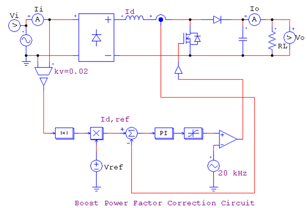
- The conventional PFC open loop circuit is as shown in Figure 1. Such a circuit structure must have a bridge rectifier and a single inductor, but it can only have a good effect when used in a small-capacity load. In the case of a large capacity load above thousand of Kw, it will generate a large voltage drop and a high ripple voltage and current, leading to a poor output voltage, harmonic interference and lowered efficiency. Hence, a better PFC power supply circuit is needed for large-capacity electrical loads. The designed PFC circuit specifications are based on the largest window-type air-conditioning on the market capacity of 2 tons, and its power requirement is about 2KW; the selected input voltage is in the range of 110V~220V, and the output voltage is increased to 400V to reduce the current load of the power supply lines, so that the design of the circuit can meet practicality. Therefore, the load resistor RL=80Ω is selected as the design goal.
 | Figure 1. Conventional PFC open loop circuit |
2.1. Characteristics of the Bridgeless Interleaved PFC Main Circuit Structure
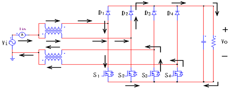
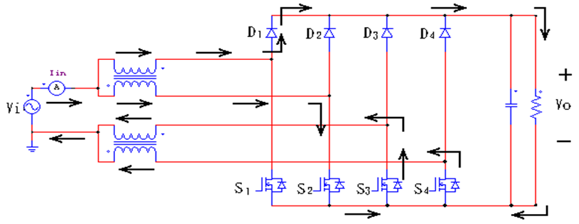
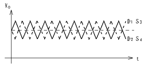
- The main driving circuit of the bridgeless interleaved PFC is as shown in Figure 2. It includes two coupled inductors; the upper coupled inductor is the primary side and the lower coupled inductor is the secondary part. The inductors control the alternating conduction of S1 and S2 in the positive half-cycle and the alternating conduction of S3 and S4 in the negative half-cycle. For example, when S1 is on, the primary side current flows through S1 and S3 to form a circuit, and the secondary side inductance current flows through D2 to the output load and back to the power source through S4, as shown by the arrows in Figure 2. The output capacitor can be charged to provide the output voltage. When S2 is on, the secondary side current flows through S2 and S4 to form the loop, and the primary side inductance current flows through D1 to the output load and back to the power source through S3, as shown by the arrows in Figure 3. During this time, the output capacitor can be recharged to provide the output voltage. During the negative half-cycle, it controls the alternating conduction of S3 and S4. The working conditions are the same as those for the positive half-cycle.
 | Figure 2. The current flow path SEM (positive half-cycle ) when S1 is on |
 | Figure 3. The current flow path SEM (positive half-cycle ) when S2 is on |
 | Figure 4. Output voltage ripple SEM |
2.2. SEM of the Control Circuit Loop Composition
- The open-loop control circuit is as shown in Figure 5. As seen, Vi(s) is the sinusoidal voltage of the input power, and Vref is the reference signal for the adjustment of the output voltage. By multiplying Vi(s) and Vref, it is possible to get the values needed to determine the output voltage. Rectifier(+) and Rectifier(-) convert the sine wave into a positive half-cycle waveform with a phase gap of 180 degrees, Vi (+) is the positive half-cycle feedback current signal, Vi (--) is the negative half-cycle feedback current signal for the adjustment of the current and the input voltage in terms of waveform, and Vo(s) is the DC 400V output voltage. The closed-loop control circuit is as shown in Figure 6. In comparison to Figure 5, the reference signal Vref and the feedback voltage Vo(s) are modified before multiplying them with Vi(s) via the PI controller to ensure the stability of the output voltage.
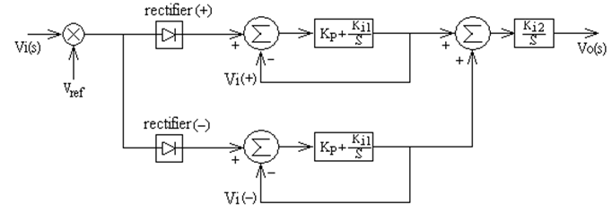 | Figure 5. Bridgeless interleaved PFC open loop control box process SEM |
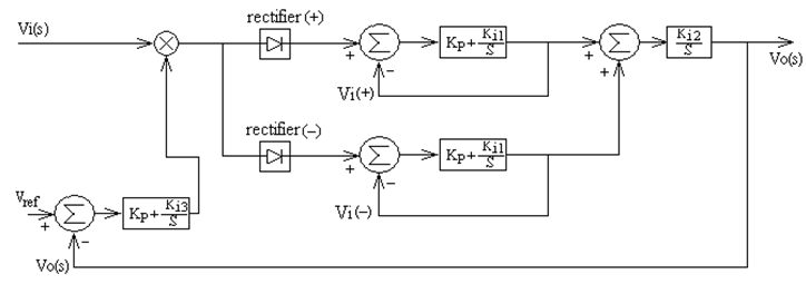 | Figure 6. Bridgeless interleaved PFC closed-loop control block processes SEM |
2.3. Bridgeless Interleaved PFC Circuit Design Structure
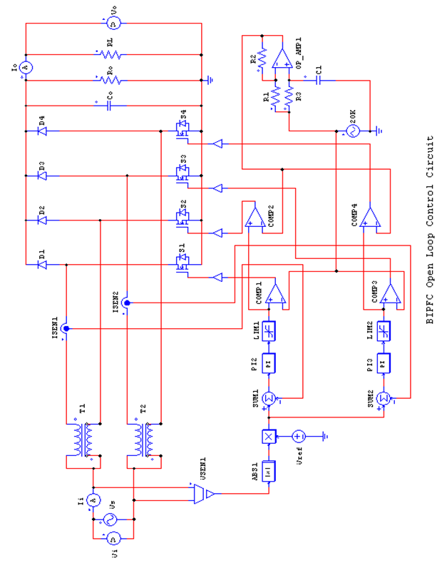 | Figure 7. Bridgeless interleaved PFC open-loop control circuit (the main circuit and the control circuit) |
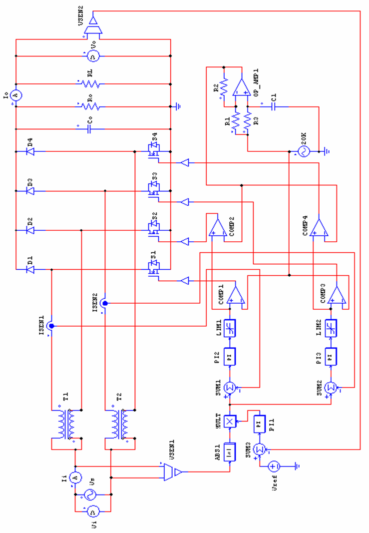 | Figure 8. Bridgeless Interleaves PFC closed-loop control circuit (the main circuit and the control circuit) |
- This study designed a 220V circuit to boost the PFC by using double coupling inductors to switch frequency through the MOSFET, which consisted of the bridgeless interleaved PFC open-loop control circuit with 400V DC voltage output, as shown in Figure 7. Although the bridgeless interleaved PFC open-loop control circuit is superior to the conventional PFC circuit and has many advantages, its tolerance is poor in the case of great changes to the load that result in unbearable voltage change rates. Therefore, the bridgeless interleaved PFC closed-loop control circuit, as shown in Figure 8, is needed to provide a stable supply to any load. The circuit has a very stable output voltage. In theory, it can maintain a set voltage output in the case of any load resistance. It is characterized by a high power factor, high efficiency and a low ripple current.
2.4. Control Circuit Description
- Figure 8 illustrates the control process of the closed-loop control circuit, as described below:1) After the reduction of input voltage Vs by Vsen1, the full wave rectification signals with a positive absolute value can be found. By multiplying the feedback voltage, the modified signal of the stable output voltage can be determined. 2) After the reduction of the output voltage Vo (S) by Vsen2, it is fed back to sum3 and added to the reference voltage Vref to obtain the modified value of the control output voltage. After being adjusted by PI1, the value is input into mult as the feedback signal to adjust the output voltage. 3) The output signals of mult are output to sum1 and sum2. After comparing the former with the positive half-cycle current feedback signal, it is amplified and adjusted by PI2 to generate the control signals that cause the current and voltage to be consistent in waveform. After comparing the later with the negative half-cycle current feedback signals, it is amplified and adjusted by PI3 to generate the control signals that cause the current and voltage to be consistent in waveform. 4) A triangular wave generator generates a triangular wave with a signal of 20KHz, which is transmitted to comp1 for the comparison with the positive half-cycle control signals to generate the 20KHz PWM sine wave control signals that switch S1. It is then transmitted to comp3 for a comparison with the negative half-cycle control signals to generate the 20KHz PWM sine wave control signals that switch S3. 20KHz triangular wave signals are simultaneously transmitted after the phase change of 180 degrees by OP-AMP1 to comp2 for the comparison with the positive half-cycle control signals, which generate the 20KHz PWM sine wave control signals that switch S2. This is transmitted to comp4 for the comparison with the negative half-cycle control signals that generate the 20KHz PWM sine wave control signals to switch S4. 5) OP-AMP1 causes a phase displacement of the 20KHz triangular wave by 180 degrees to provide the alternating driving signals to S1 and S2, and to S3 and S4, in order to realize the alternating conduction of S1 and S2, and S3 and S4. 6) The power input end Vi and Ii, and the output end Vo and Io, are meters to measure voltage and current, and thus they have no impact on the circuit.
3. Design Circuit Simulation Characteristics
3.1. Conventional PFC Simulation Results
- Figure 1 illustrates the conventional PFC (single MOSFET boost) circuit. The results of simulating the capacity for a window type air conditioner of about 2000W are as shown in Figure 9, where Vi is the input voltage, Vo is the output voltage, and Ii is the input current. According to the simulation results, the maximum input voltage was 220V, the maximum input current was 19.5A, the output voltage was DC 400V, the power factor was close to 1, the output voltage ripple was 20Vp-p, the input current ripple was 2.5Ap-p, the calculated efficiency was 0.93%, and the output voltage was stabilized at 0.36 seconds.
3.2. Simulation Characteristics of the Open-loop Bridgeless Interleaved PFC Circuit
- The proposed open-loop bridgeless interleaved PFC circuit is shown in Figure 7. As shown in the figure, the parameters of controller PI1 are Gain 1, time constant 0.03. Parameters of PI2 and PI3 are Gain 2, time constant 0.03, parameters of Sum1~Sum3 are Gain (+) 1, Gain(-) -1, parameter of Vsen1 is Gain 0.02 The simulation results of providing the capacity for a 2000W window type air conditioner with the same capacitor and inductance parameters as the conventional PFC circuit are as shown in Figure 10, where Vi is the input voltage, Vo is the output voltage, and Ii is the input current. According to the results, the maximum input voltage was 220V, the maximum input current was 19A, the output voltage was 400V DC, the power factor was close to 1, the output voltage ripple was 15Vp-p, the input current ripple was 2Ap-p, the calculated efficiency was 95.6%, and the output voltage was stabilized at 0.12 seconds.
3.3. Simulation of Characteristics of the Closed- loop Bridgeless Interleaved PFC Circuit
- The proposed closed-loop bridgeless interleaved PFC circuit is shown in Figure 8. Parameter of Vsen2 is Gain 0.03 The simulation results of providing the capacity for a 2000W window type air conditioner with the same load of 2000W (RL=80Ω) are shown in Figure 11(a) to Figure 11(d). As shown in Figure 11(a), the output voltage was stabilized at 0.12 seconds. Figure 11(b) shows that the maximum input voltage was 220V, the maximum input current was 19A, the output voltage was DC 400V, and the power factor was close to 1. Figure 11(c) shows that the output voltage ripple was 12Vp-p. Figure 11(d) shows that the input current ripple was 1Ap-p and the calculated efficiency was 96%.The simulation results for changing the load resistance to RL=180Ω are shown in Figure 12. The output voltage remained at 400V, the ripple voltage was reduced to Vr=4V, the input current was reduced to 6.7A, the ripple current Ir=1Ap-p, the efficiency η=90, and the power factor was close to 1.
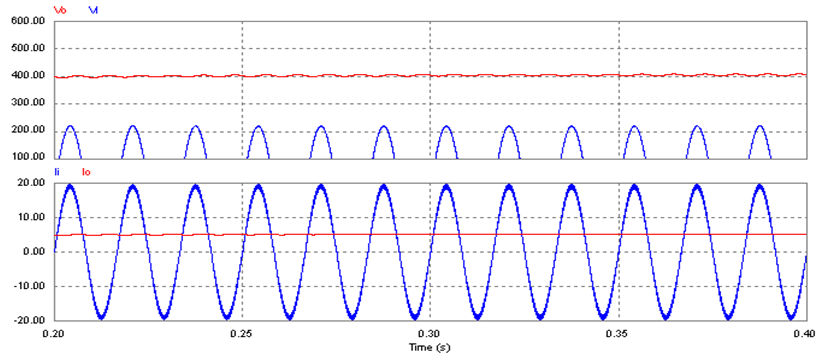 | Figure 9. Simulation results of the conventional PFC control circuit |
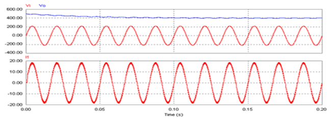 | Figure 10. Simulation results of the open-loop bridgeless interleaved PFC circuit |
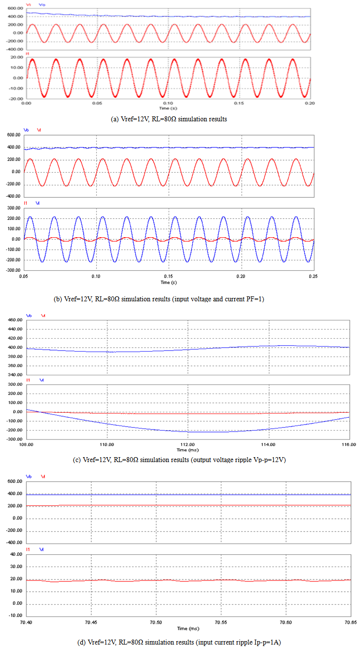 | Figure 11. Simulation results of the closed-loop BIPFC circuit, in the case of a load of 2000W (RL=80Ω) |
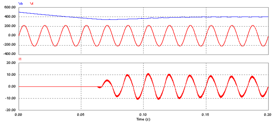 | Figure 12. Simulation results of the closed-loop bridgeless interleaved PFC circuit (Rl=180Ω) |
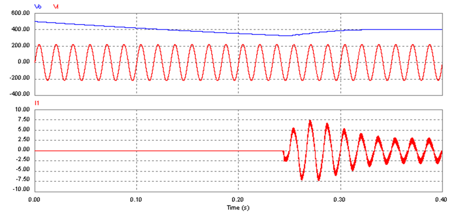 | Figure 13. Simulation results of the closed-loop bridgeless interleaved PFC circuit (Rl=580Ω) |
- The simulation results for changing the output resistance to RL=580Ω are shown in Figure 13. The output voltage remained at 400V, the ripple voltage was reduced to Vr=0.5Vp-p, the input current was reduced to 1.9A, the ripple current Ir=0.6Ap-p, the efficiency η=92.8, and the power factor was close to 1. As seen, the proposed circuit was adaptive to any change in the load and could provide a stable and high quality DC power supply.
4. Implementation and Testing Results
4.1. Implementation of the Circuit Structure
- The physical device of the closed-loop bridgeless interleaved PFC circuit is shown in Figure 14. Its main circuit included two 0.1mH coupling inductors, a 1000μF 500V capacitor, four IXFN48N50 MOSFET transistors and four 30A 500V rectifiers. A HULL Sensor was used to capture the current signals. A transformer was used to receive the AC input voltage signals and the resistance subvoltage is to get the signals of the output voltage.
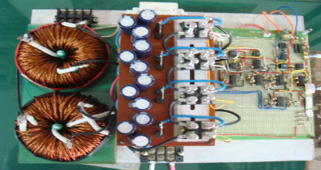 | Figure 14. Picture of the physical entity of the closed-loop bridgeless interleaved PFC circuit |
4.2. Testing Results
4.2.1. Control Circuit Testing Results
- The gate excitation signals of S1 and S2, and S3 and S4 without a load are shown in Figure 15(a) and (b). Figure 15(a) illustrates the excitation signal of S1 and S2, which guides the alternating conduction of S1 and S2 using a phase gap of 180 degrees to realize the induction of coupling inductor L of the output voltage. Figure 15(b) illustrates the excitation signal of S1 and S3, which guides the alternating conduction of S1 and S2 using the excitation signals of S1 and S2 in the positive half-cycle of the sine wave of the input power supply, and which guides the alternating conduction of S3 and S4 using the excitation signals of S3 and S4 in the negative half-cycle of the sine wave of the input power supply.
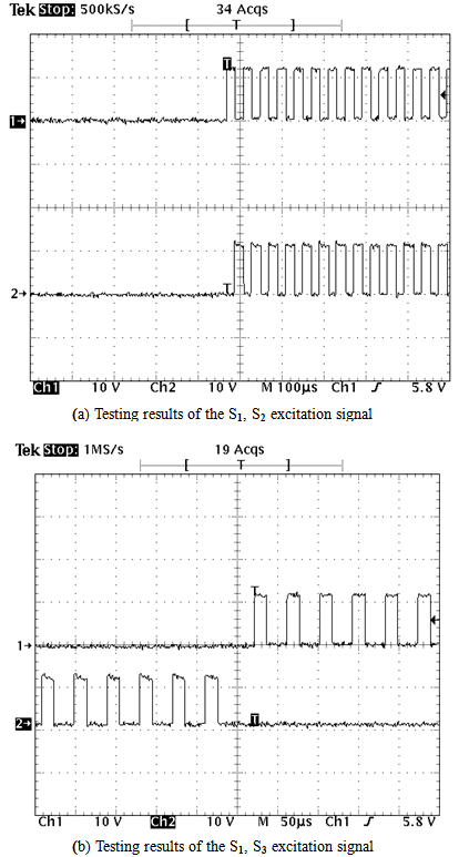 | Figure 15. Testing results of the excitation signals of S1, S2, S3 and S4 without a load |
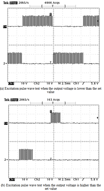 | Figure 16. Testing results of the excitation signals of S1, S2, S3 and S4 with a load |
4.2.2. Testing Results of Input and Output in the Case of Different Loads
- When the input voltage is 220Vm, the load resistance is 1000Ω, and the output voltage is adjusted to 400V, the waveforms of the output voltage and current are as shown in Figure 17(a), which shows that the voltage was 400V DC, the current was 0.4A, the output power Po was 160W (see equation 1) and there was no ripple change. The waveforms of the input voltage and the current can be found in Figure 17(b), which shows that the voltage was 220Vm and the current was 1.6A Im. The waveforms of the voltage and the current were nearly at the same phase; therefore, the power factor approached 1. In addition, the input power Pi was 176W (see equation 2); therefore, the efficiency η was 90.9% (see equation 3).
 | (1) |
 | (2) |
 | (3) |
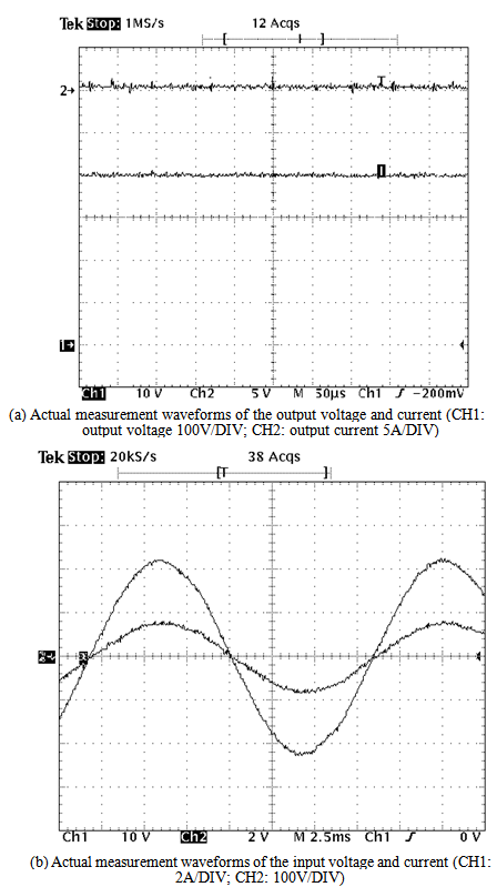 | Figure 17. Testing results of the BIPFC circuit with a load of 160W (RL=1000Ω) |
 | (4) |
 | (5) |
 | (6) |
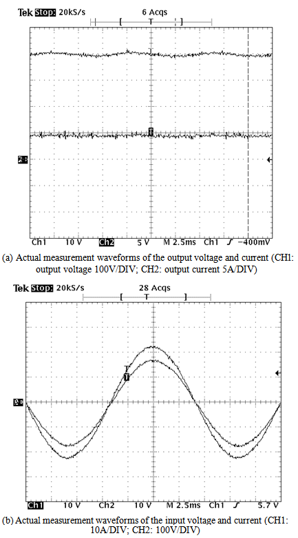 | Figure 18. Testing results of the BIPFC circuit with a load of 1720W (RL=93Ω) |
 | (7) |
 | (8) |
 | (9) |
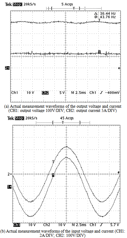 | Figure 19. Testing results of the BIPFC circuit with a load of 2480W (RL=63Ω) |
5. Results and Discussion
- The designed circuit simulation results are shown in Figure 11(a) to Figure 11(d). As shown in Figure 11(a), the output voltage was 400V DC, was very stable with an extremely small ripple voltage, and had an output power Po=2000W. Figure 11(b) shows that the input voltage Vi=220Vm, the input current Iim=19A, the input voltage and the input current were at the same phase, the power factor PF=1, and the input power Pi= (220V×19A)÷2 = 2090W; therefore, the efficiency was η=2000W÷2090W = 95.7%. According to the above simulation results, the designed circuit had excellent performance; in particular, it could maintain extremely small voltage and current ripple factors in the case of a large load output while maintaining excellent efficiency and power factors. The testing results of the physical implementation of the circuit are shown in Figures 17 to 19. It can be learnt from the figures that the actual measurement results were consistent with the simulation results in terms of the power factor, voltage, and current ripple. However, the efficiency was only 94.7% and was 1% short of the simulation results. The possible causes may have been due to circuits requiring further simplification, an inaccurate inductor design, or testing errors. Using DSP to control these errors could result in the realization of 96% efficiency.
6. Conclusions
- The proposed DC bridgeless interleaved PFC circuit was shown to have excellent performance by the simulation results and the actual testing results. It was found to have good PFC functions, as the simulation results showed that the input voltage and the input current were at the same phase; hence, the power factor approached 1. The bridgeless rectification circuit could reduce the power loss from the rectification and could improve the conversion efficiency by more than 94%. The interleaved switch boosting technology could substantially reduce the input ripple current to 0.8A, which is about one-fifth that of conventional circuits. The output ripple voltage was reduced by about one quarter as compared with the same type of conventional circuits. Lastly, the tolerance to the change in the output load (the voltage adjustment rate) was very good. The above benefits confirmed that before new energy sources can replace conventional ones, the active development of power saving technology is still the most direct and important option. Hence, the development of the proposed circuit could provide great contributions to energy saving and carbon reduction.
ACKNOWLEDGEMENTS
- The authors would like to thank National Taipei University of Technology and Ming Hsin University of Science and Technology for providing a research environment and all of the required instruments and materials. Thanks are also given to Prof. C.S. Tseng, Associate Prof. C.T. Huang, and Associate Prof. M.F. Tsai, for their help in the successful completion of this paper.
 Abstract
 Reference
 Full-Text PDF
 Full-text HTML