-
Paper Information
- Paper Submission
-
Journal Information
- About This Journal
- Editorial Board
- Current Issue
- Archive
- Author Guidelines
- Contact Us
International Journal of Electromagnetics and Applications
p-ISSN: 2168-5037 e-ISSN: 2168-5045
2020; 10(1): 19-29
doi:10.5923/j.ijea.20201001.03
Received: Oct. 12, 2020; Accepted: Oct. 28, 2020; Published: Nov. 15, 2020

Performance Analysis of an Inset-Fed Circular Microstrip Patch Antenna Using Different Substrates by Varying Notch Width for Wireless Communications
 Abstract
 Reference
 Full-Text PDF
 Full-text HTML
Md Ziaur Rahman 1, Kartik Chandra Deb Nath 2, Mohammed Mynuddin 3
1Department of Civil Engineering, Dhaka International University, Dhaka, Bangladesh
2Department of Physics, Govt. Shah E-Tebaria College, Talora, Bogura, Bangladesh
3Department of Electrical and Computer Engineering, Georgia Southern University, GA, USA
Correspondence to: Md Ziaur Rahman , Department of Civil Engineering, Dhaka International University, Dhaka, Bangladesh.
| Email: |  |
Copyright © 2020 The Author(s). Published by Scientific & Academic Publishing.
This work is licensed under the Creative Commons Attribution International License (CC BY).
http://creativecommons.org/licenses/by/4.0/

This paper demonstrates the effect of using different dielectric substrates on the performance of an inset fed circular patch microstrip antenna with the variation of notch width for 5 GHz wireless communications. The design frequency and the thickness of the substrates were kept constant while different substrate materials were used and the notch width was varied to obtain the maximum performance. Four Substrate materials like Arlon AD 350A with dielectric constant of 3.5, FR-4 with dielectric constant of 4.3, Preperm L500 with dielectric constant of 5 and Lead glass with dielectric constant of 6 were taken to investigate their effects on the performance by simulating the antenna at 5GHZ. It was seen that among the four dielectric materials, the substrate with the low dielectric constant has the highest directivity with a wide beam radiation pattern while FR 4 has the least gain. Maximum negative return loss of -57.32 was obtained for Preperm L500 dielectric material. The proposed antenna can efficiently be used in C band applications like in satellite communication, WiMAX, WLAN, Wi-Fi, WiMAX and so on for transmitting and receiving signals and information over the long distances by dissipating less amount of power.
Keywords: Inset-fed, Circular patch, Notch width, Return loss, VSWR, Patch antenna, Directivity, CST MWS
Cite this paper: Md Ziaur Rahman , Kartik Chandra Deb Nath , Mohammed Mynuddin , Performance Analysis of an Inset-Fed Circular Microstrip Patch Antenna Using Different Substrates by Varying Notch Width for Wireless Communications, International Journal of Electromagnetics and Applications, Vol. 10 No. 1, 2020, pp. 19-29. doi: 10.5923/j.ijea.20201001.03.
Article Outline
1. Introduction
- In recent years, the microstrip patch antenna has widely been used for various specific applications in satellite communications, aerospace, radars, biomedical applications, mobile communication for GSM, and remote sensing applications [1] because of its special features like ease of analysis and fabrication, low cost, light weight, easy to feed, capability of dual, triple and several frequency operations and attractive radiation [2]. Although the patch antenna has several advantages but it has some limitations like narrow bandwidth [3]. The need for wideband antennas operating at higher frequencies is significantly increasing as the various wireless applications require more and more bandwidth [4]. To meet the growing demands of the communication systems, researchers have continuously developed new and effective methods to improve the different features of microstrip patch antennas like bandwidth [5]-[7], polarization [8], gain [9], return loss, directivity etc. The microstrip antennas are predominantly a broadside radiator [10]. The Patches of the radiating elements of printed antennas have different shapes like triangular, rectangular, square, elliptical and circular [11-12]. However, circular structures have been found to be smaller dimensions related to the operations of the frequency [13]. It is very easy and simple to design and control the radiation patterns in circular patch antenna as compared to the rectangular antenna where length and width of the patch are used to control and design [14]. Moreover, at the same design frequency the circular patch antenna is about 16% smaller in size than that of the rectangular patch antenna [15]. The patch of antenna is a thin metal strip mounted on the ground plane under which the thickness of the metal strip is limited by t <<λ0 and the height is restricted by 0.00033 λ0 < h < 0.053 λ0 to reduce the fringing effect and the range of dielectric constants are usually in the range of 2.2 <εr <12 [16-17]. For this reason, it is extensively being used for the various wireless applications. Thicker substrates with lower values of dielectric constant provide better efficiency, larger bandwidth, increase the fringing field of the patch and thus the radiating power, but it increases weight and surface wave losses [18]. Higher dielectric constants of thin substrates are attractive for microwave circuitry since they need tightly bound fields to minimize undesirable radiation and coupling, which lead to smaller element sizes; however, they are less efficient and have relatively smaller bandwidths [18]. There are different types of feeding techniques of a patch antenna like: probe feed, microstrip line feed, aperture coupled feed and proximity coupling feed [19]. The proposed antenna is fed by 50Ω microstrip transmission line [2] since it is most commonly being used and very easy to design. The fed is inserted into the circular radiating element for proper impedance matching. In our study, by introducing a slot into the circular patch we have varied the notch width g using various dielectric substrates to improve the performance of circular patch antenna. Ideally, the distance between the two slots should be λ/2, where λ is the wavelength in the dielectric (substrate). But the actual separation of the two slots is kept slightly less than λ/2. The basic structure of an inset feed circular patch antenna is shown in figure-1:
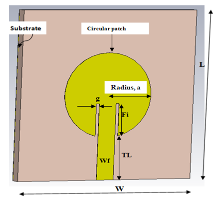 | Figure 1. Basic structure of an inset feed circular patch antenna |
2. Design Equations of the Circular Patch Antenna
- i) Calculation of radius of the circular patch:
 | (1) |
 ii) Calculation of length and width of the substrate: According to [20], the length and width of the substrate are normally taken two times the radius of the circular patch.L = 2 × Patch Diameter = 2 × (2a)W = 2 × Patch Diameter = 2 × (2a)iii) Calculation of effective dielectric constant (εreff):
 | (2) |
 | (3) |
 | (4) |
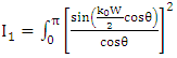
 And G12 is calculated as
 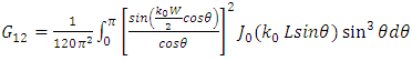 | (5) |
 function varies very rapidly and the inset feed distance Fi is calculated as:
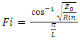 | (6) |
 can be calculated using the formula [21]:
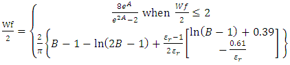 | (7) |
 Where,
 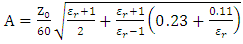 and
and  The above equations are solved using Matlab and the antenna dimensions are determined.
3. Results and Discussions
- In this paper an inset fed circular microstrip patch antenna using different dielectric substrates is designed and simulated using CST. This program analyzes the 3D and multilayer configurations general form. It is commonly used for the design of different types of antenna. It may be used to calculate and plot the return loss, standing wave ratio from Smith charts, Real power Vs Frequency, VSWR, E-field and H-field distribution, gain as well as radiation patterns. The antenna dimensions for the dielectric materials of Arlon AD 350A with dielectric constant of 3.5, FR-4 with dielectric constant of 4.3, Preperm L500 with dielectric constant of 5 and Lead glass with dielectric constant of 6 are determined and the antenna performances are investigated by varying the notch width for the circular patch antenna. The bandwidth of the antenna is defined for that range of frequencies over which the RL is less than -10dB corresponds to the value of VSWR keeping less than 2 and it is calculated according to [1].
3.1. Performance Anlysis Using Arlon AD 350 Dielectric Material with Dielectric Constant 3.5
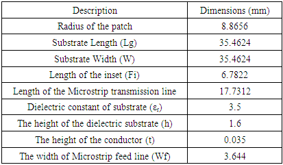
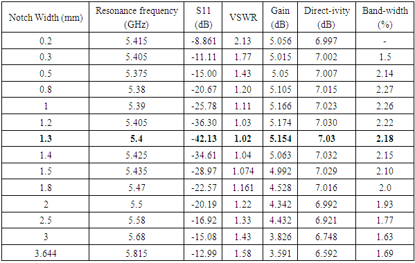
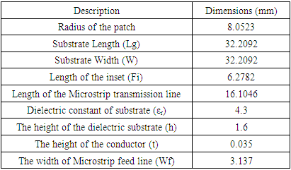
- For the dielectric material of Arlon AD 350 the radius of the patch is calculated as 8.8656 mm and the inset feed distance is Fi=6.7822 mm. The width of the microstrip transmission line (Wf) is taken equal to 3.644mm. The dimensions of the proposed antenna for Arlon AD 350 dielectric material is shown in table-1.
|
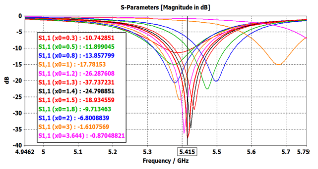 | Figure 2. The return loss, S11 of the designed antenna at resonant frequency 5.415 GHz with varying g for the dielectric constant 3.5 |
|
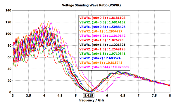 | Figure 3. VSWR of the designed antenna at resonant frequency 5.415 GHz with varying g for the dielectric constant 3.5 |
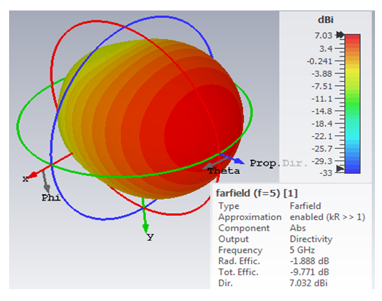 | Figure 4. Directivity of the designed antenna at resonant frequency 5GHz for g=1.3mm |
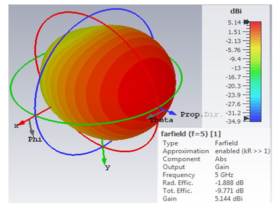 | Figure 5. Gain of the designed antenna at resonant frequency 5GHz for g=1.3mm |
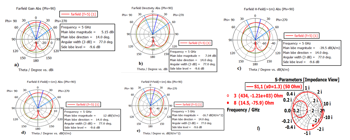 | Figure 6. Farfield radiation pattern of the designed antenna: a) gain b) directivity c) H-field d) E-field e) Power field and f) Smith chart at resonant frequency 5GHz |
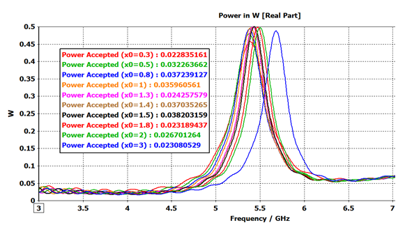 | Figure 7. Accepted power of the antenna with varying g |
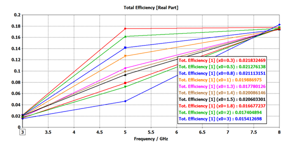 | Figure 8. Total efficiency of the proposed antenna with varying g |
3.2. Performance of the Antenna Using FR-4 Dielectric Material with Dielectric Constant 4.3
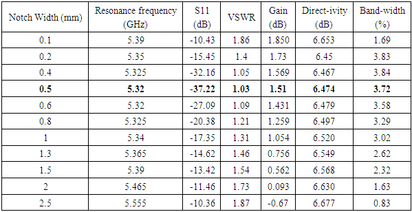
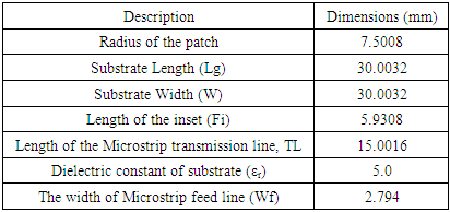
- The dimensions of the antenna for FR-4 substrate is shown in table-3. The radius are calculated as 8.0523 mm and the inset feed length is found equal to 6.2782. While increasing the notch gap g from 0.1 mm, it is found that return loss S11 and VSWR significantly started to decrease gradually and after reaching at a value these parameters experienced the reverse case with further increase in g. The resonating frequency varies from 5.39 GHz to 5.55 GHz and the lowest values of S11=-37.22 and VSWR=1.03 are found at the resonating frequency of 5.32 GHz which is little smaller than for that of the Arlon AD 350 dielectric material.
|
|
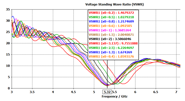 | Figure 9. VSWR of the designed antenna at resonant frequency 5.32 GHz with varying g for the dielectric constant 4.3 |
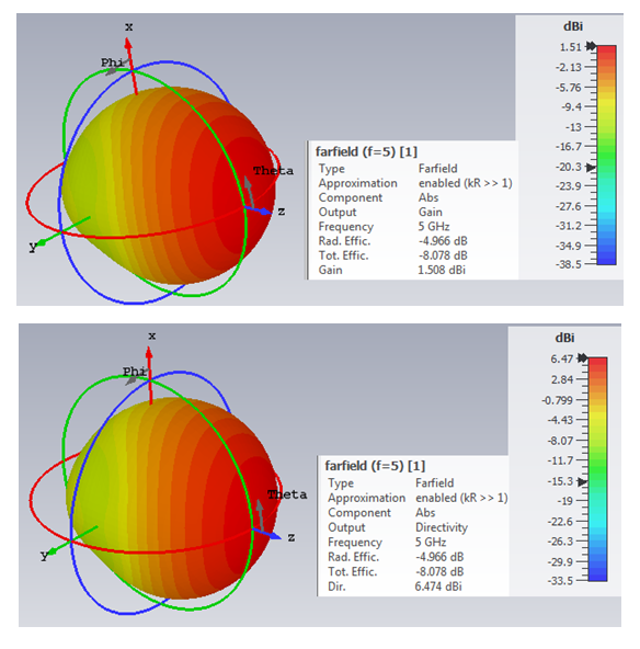 | Figure 10. Gain & Directivity of the designed antenna at resonant frequency 5GHz for g=0. 5mm |
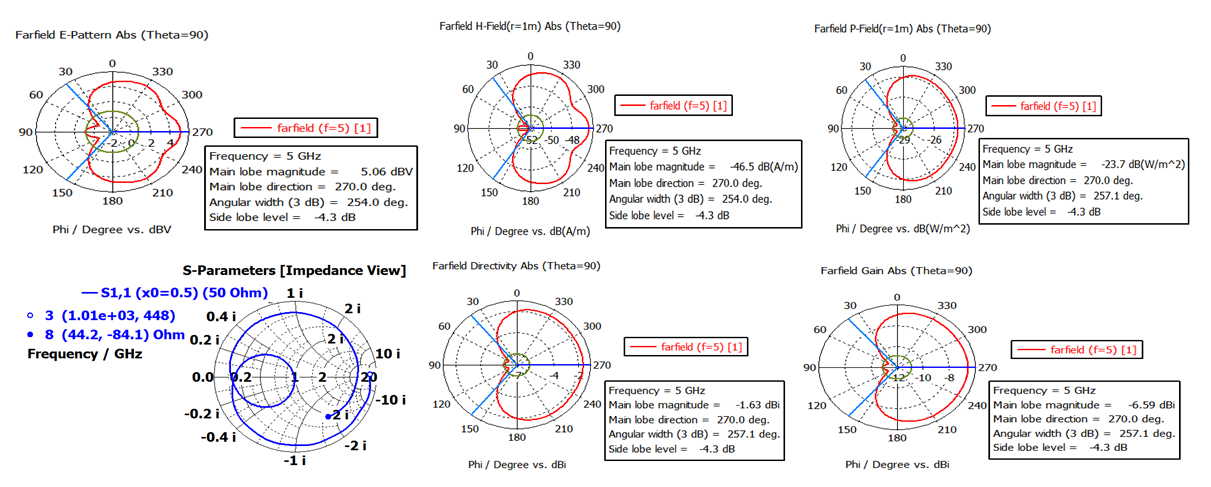 | Figure 11. Farfield radiation pattern of the designed antenna: a) E-pattern b) H-field c) Power field e) directivity f) gain and d) Smith chart at resonant frequency 5GHz |
3.3. Performance of the Antenna Using Preperm L500 Dielectric Material with Dielectric Constant 5.0
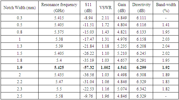
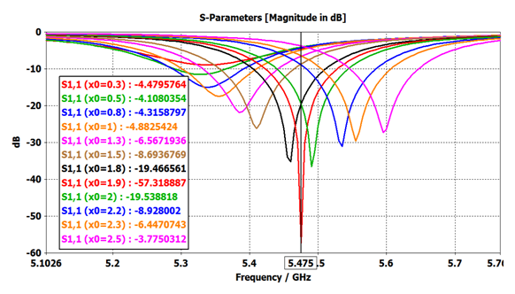
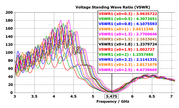
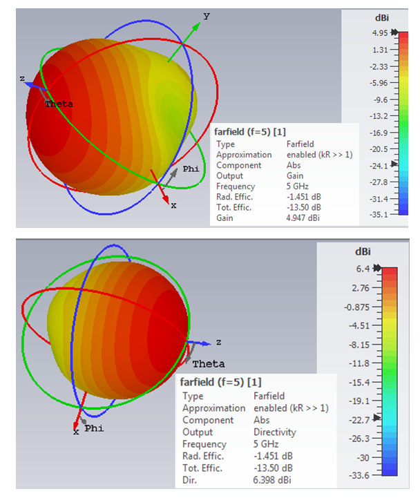
- The radius of the antenna which is the only parameter to design and to control the radiation pattern is calculated as 7.5008 mm for Preperm L500 substrate. The antenna dimensions designed using for εr =5 is shown in table-5. It is noticed that for the thin dielectric material with higher value of dielectric constant the radius, Wf and other parameters also decreases since these parameters depend on the radius of the circular patch. Likewise, Arlond AD 350 and FR-4 dielectric materials, using Preperm L500 as the dielectric material the return loss S11 and VSWR decrease simultaneously with increasing g and after attaining at their lowest level for a certain value of g, S11 and VSWR again start to increase with further increased in g. The lowest value of the return loss and VSWR are found as -57.32 dB and 1.002 respectively as shown in table-6 for the notch width, g=1.9 mm which indicates that the input impedance is highly matched with the radiating patch and very less amount of energy is lost while transferring the power to the patch which is highly expected for the most of the wireless communication applications. The return loss S11 and VSWR are taken at resonant frequency of 5.475 GHz with the variation of g shown in fig-12 and fig-13. But in table-6, the antenna performance parameters are taken in accordance to their individual resonant frequencies and for that reason the values of S11 and VSWR are different than from fig.12 and fig.13. The directivity also increases with the variation of g and maximum value of it is observed as 6.342 dB. At resonating frequency 5.39 GHz, the maximum gain and bandwidth of 5.235 dB and 2.04 % are found for g=1.9 mm. At resonant frequency 5.475GHz, the S11 and VSWR are very high for the value of g from 0.3mm-1.5 mm and it again becomes high when g is taken above 1.9 mm. This is because in these ranges of g, the input impedance does not match with the radiating patch impedance and the resonant frequency is shifted but the parameters are taken at 5.475 GHz. The smith chart of the designed antenna is shown in fig.14 for g=1.9 mm. The main lobe magnitude (Phi=90) of the far field directivity and E-field are 6.4 dBi and 7.68dB (v/m) respectively which are good for the usage of the antenna in various wireless communication applications.The highest accepted power is found to be 0.499 W for the notch width, g=1.9mm. The polar plot of the proposed antenna suggests that is may efficiently be used for the transmitting and receiving the signal and information to the remote distances with the minimum loss of energy.
|
|
 | Figure 12. The return loss, S11 of the designed antenna at resonant frequency 5.32 GHz with varying g for the dielectric constant 4.3 |
 | Figure 13. VSWR of the designed antenna at resonant frequency 5.475 GHz with varying g for the dielectric constant of 5.0 |
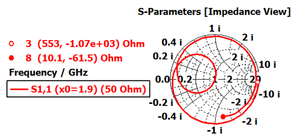 | Figure 14. Smith chart of the designed antenna at resonant frequency 5GHz for g=1.9 mm |
 | Figure 15. Gain & Directivity of the designed antenna at resonant frequency 5GHz for g=1.9 mm |
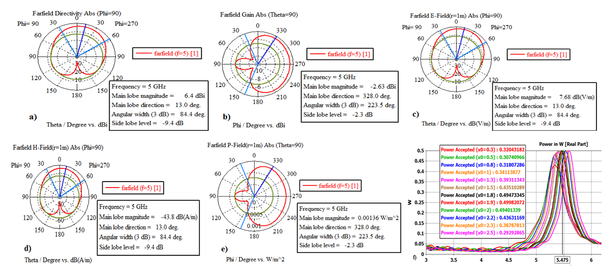 | Figure 16. Farfield radiation patterns of the designed antenna: a) directivity b) gain c) E-field d) H-field e) power field and f) accepted power of the antenna designed with Preperm L500 dielectric material with dielectric constant 5.0 |
3.4. Performance of the Antenna Using Lead Glass Dielectric Material with Dielectric Constant 6.0
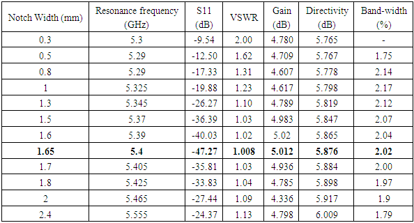
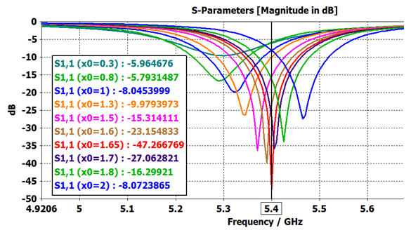
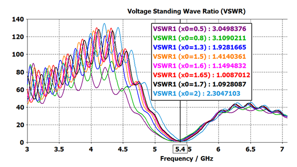
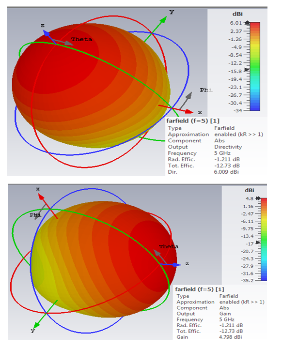
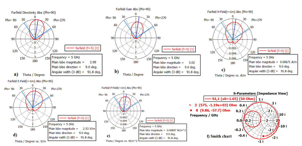
- Using Lead glass as the dielectric substrate the radius and the width of the transmission line are fond to be as 6.811 mm and 2.4101 mm respectively as shown as in table-7. The resonance frequency is shifted from 5.29 GHz to 5.555 GHz with the variation of notch width g from 0.3 mm to 2.4 mm. It is observed that at g=1.6 the return loss S11 is -40.03 dB but with very little increase in g at 1.65 mm the return loss significantly drops to -47.27dB. This is because at g=1.65 mm better impedance matching is obtained and less amount of energy is lost while transferring energy to the radiating patch. The return loss S11 and VSWR decreased up to a limit with increasing the value of g and after this point of g the return loss and VSWR started to increase due to mismatch of the impedance. The radiation pattern and polar plot for g=1.65 is shown in fig-19 and fig-20. There is little increase in directivity with increasing g and maximum value 6.009 dB is found at g=2.4 mm. The maximum gain and bandwidth obtained using lead glass as the dielectric substrate are 5.02 dB and 2.17 dB respectively. The characteristics of the antenna are shown in table-8.
|
|
 | Figure 17. The return loss, S11 of the designed antenna at resonant frequency 5.4 GHz using lead glass with varying g |
 | Figure 18. VSWR of the designed antenna at resonant frequency 5.4 GHz with varying g for the dielectric constant of 6.0 |
 | Figure 19. Directivity & Gain of the designed antenna at resonant frequency 5GHz for g=1.65 mm |
 | Figure 20. Farfield radiation pattern (polar plot) of the designed antenna: a) directivity b) gain c) H-field d) E-field e) power field and of the antenna designed using Lead glass with dielectric constant 6.0 |
4. Conclusions
- The effect of using different substrates on the performance of an inset feed circular microstrip antenna by varying their notch width has been studied. The resonance frequency of the antenna showed negligible shift for different dielectric materials. Likewise, rectangular patch antenna analyzed by [21], in circular patch antenna the return loss and VSWR at first started to decrease up to a level with increasing the value of notch width g and above this value of g, the S11 and VSWR started to increase again for further increased the value of g. The dimension of the antenna also decreases for the higher values of the dielectric constants. Among the used four dielectric materials, FR-4 has the minimum gain (1.51dB) but it showed the highest bandwidth (3.72%). Simulating the antenna at the same frequency at 5GHz, the lowest amount of S11=-57.32 dB and VSWR=1.002 were obtained for Preperm L500 dielectric substrate which can successfully be used for the various wireless communication applications due to having very less amount of energy losses while transferring power to the radiating patch. The equation (6) used for calculating the inset feed distance (Fi) in rectangular patch antenna by [2] can also efficiently be used in circular patch antenna to calculate the inset feed distance (fi). It can be concluded that using thicker dielectric materials with their low values maximum gain and directivity are obtained. The overall performance of the circular patch antenna is significantly influenced by the different substrate materials. For C band applications at 5GHz frequency, Preperm L500 dielectric material can fruitfully be used to design the antenna ensuring the minimum loss of energy while transmitting and receiving signal to the remote distances. Moreover, for obtaining the best performance in circular patch antenna, proper impedance matching is very crucial. Since, in circular patch antenna the only controlling parameter is the radius of the patch so for the required resonant frequency the substrates material should be selected at the proper way. The VSWR and the return loss are also dependent on the inset feed length, transmission line length and the notch gap and its values also vary for various dielectric materials so it ought to be calculated very cautiously for ensuring the proper impedance matching by using the above mentioned mathematical formula.