-
Paper Information
- Paper Submission
-
Journal Information
- About This Journal
- Editorial Board
- Current Issue
- Archive
- Author Guidelines
- Contact Us
International Journal of Electromagnetics and Applications
p-ISSN: 2168-5037 e-ISSN: 2168-5045
2019; 9(1): 1-6
doi:10.5923/j.ijea.20190901.01

Optimizing the Absorption Capability of a Microbolometer Pixel’s Active Element
 Abstract
 Reference
 Full-Text PDF
 Full-text HTML
C. Bolakis1, 2, I. S. Karanasiou3, D. Grbovic4, C. Vazouras2, G. Karunasiri4, N. Uzunoglu1, 3
1National Technical University, School of Electrical and Computer Engineering, Athens, Greece
2Hellenic Naval Academy, Sector of Combat Systems, Naval operations, Electronics & Telecommunications, Piraeus, Greece
3National Technical University, Institute of Communication and Computer Systems, Athens, Greece
4Naval Postgraduate School, Department of Physics, California, United States of America
Correspondence to: C. Bolakis, National Technical University, School of Electrical and Computer Engineering, Athens, Greece.
| Email: |  |
Copyright © 2019 The Author(s). Published by Scientific & Academic Publishing.
This work is licensed under the Creative Commons Attribution International License (CC BY).
http://creativecommons.org/licenses/by/4.0/

In this paper, we propose a new approach for effective detection of THz and IR radiation, using a configuration of a thin metal and semiconductor layers. We present the design and performance of an effective absorber of radiation that can be used as the active pixel element of a microbolometer. A double-layered absorber, comprising a thin metal layer placed onto a poly-Si substrate was designed through a fine-tuning process. The results indicate that the proposed low-cost, double-layered absorber can be tuned based on the metal layer sheet resistance and the thickness of various poly-Si media. This can be done in a way that takes advantage of the diversity of the absorption of the metal films over the THz spectrum (0.1 - 10 THz) and both the mid and long wavelength IR region (3 - 14μm). A ‘’wide-spectrum linear equation’’ has been developed, having as input any discrete wavelength with desired absorption peak in the THz or IR spectrum and as output the appropriate thickness of the poly-Si medium. It was found, using this equation, that the composite absorber retains the ability to absorb 96% and reflects less than 1% of the incident power of radiation. Moreover, based on the fact that both layers of the absorber can be used as active element of a microbolometer pixel, a ‘’hybrid’’ nature of the designed absorber emerges. To this end, we compare important metrics and design complexity between the ‘’hybrid’’ absorber and a state-of-the-art microbolometric pixel element comprised either of a thin metal layer or a material with high TCR. The analysis shows that the developed absorber can be considered a promising candidate for integration into current and sophisticated microbolometer configurations.
Keywords: THz / IR spectrum, Microbolometer, Fine-tuned, Hybrid, Active pixel element, Wide-spectrum linear equation
Cite this paper: C. Bolakis, I. S. Karanasiou, D. Grbovic, C. Vazouras, G. Karunasiri, N. Uzunoglu, Optimizing the Absorption Capability of a Microbolometer Pixel’s Active Element, International Journal of Electromagnetics and Applications, Vol. 9 No. 1, 2019, pp. 1-6. doi: 10.5923/j.ijea.20190901.01.
Article Outline
1. Introduction
- Microbolometer arrays - comprising micro-scale pixels, whose resistance is highly sensitive to changing temperatures, - have proven to be an effective basis for real-time infrared imaging systems [1]; Because this technology is based upon temperature-driven changes in pixel resistivity, produced by the absorption of incident photons (rather than electron-hole generation/recombination, as in most semiconductor-based photodetectors), the devices are not susceptible to thermal excitation and can be routinely operated at room temperature [1]. Researchers at the Massachusetts Institute of Technology (MIT) and the Naval Postgraduate School (NPS) have independently shown that they are likewise sensitive to radiation at terahertz frequencies [2-5]. The relatively short thermal time constant (~10 ms) of the microbolometer focal plane array (FPA) allows real-time imaging at TV frame rates (~30 Hz). Nearly all such cameras are designed and engineered for use in the infrared regime (typically 8-14 μm).Under normal operation in the infrared regime, gray body radiation - originating from objects within the camera’s field of view - falls upon the FPA; Based on the fact that the Noise Equivalent Temperature Difference (NETD) of most microbolometers is less than 0.1 K in the infrared regime [6], microbolometers can easily produce high-resolution images that clearly distinguish persons from their background and, from their clothing as well. In previous work, the design and characterization of terahertz absorbing nano-laminates of dielectric and metal thin films was presented [7]. Initially, a terahertz-absorbing thin-film stack, containing a dielectric Bragg reflector and a thin chromium metal film, was fabricated on a silicon substrate for applications in bi-material terahertz (THz) sensors. The optimized absorption was found to be about 50% for a particular metal film thickness [7]. As a continuation of the effort to increase the absorption results at the THz range, an optimized absorber of a thin metallic layer located on a glass medium, which could be integrated into a microbolometer, was presented [8]. In this paper, further optimization, for more effective and broadband detection of the incident radiation, is proposed. Use of poly-silicon thin layers; the post-optimization process and performance of an absorber that can be used as the active element of a microbolometer pixel, is presented.
2. Materials and Methods
- In thermal detection mechanism, the absorbed radiation by a thermal detector causes its temperature to rise. That rise can be detected using a temperature-sensitive element. The wavelength response of thermal detector is determined by the infrared-absorbing material. With the proper choice of absorber, thermal detectors can achieve uniform response for all the distinct wavelengths of interest. In addition, a setup and a theoretical analysis of a special double-layered absorber is following.
2.1. Absorber Setup
- In our previous work, an effective double-layered absorber, consisting of a metal and a glass layer, showed promise for microbololometer integration [8]. The transmittance (T) of a metal film is the same, regardless of the direction in which it is measured (from metal side or the glass side). This is not the case for reflectance (R), which if measured at the glass side, is slightly lower than when measured at the metal side. Since T+R+A=1, the reduction in reflectance at the glass side means that the absorptance (A) from that side must be higher [8]. In addition, the modification process targeting the substitution of the glass layer by a material with temperature coefficient of resistance (TCR), could further improve microbolometer performance. Instead of only metal being sensitive to temperature change, both the metal and the substrate would be sensitive to temperature change.The absorber presented in this paper is designed as a thin layer of metal, located on a high TCR material (diluted poly-Si). With incorporation of a Rare-earth element (i.e. Europium), the TCR of poly-Si can reach values as high as 0.187 Κ-1 [9]. The schematic is illustrated in Fig. 1.
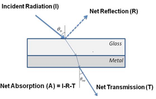 | Figure 1. Schematic of the absorber, positioned to the incidence radiation |
2.2. Analytical Approach
- Absorption of electromagnetic radiation in a thin metal film, located on a poly-Si medium, can be calculated by determining transmission and reflection, taking into account multiple reflections at each interface of the double-layered absorber as illustrated in Fig. 2 and explicitly described in [8, 13]. The absorption is then estimated by subtracting transmission and reflection from the unity.
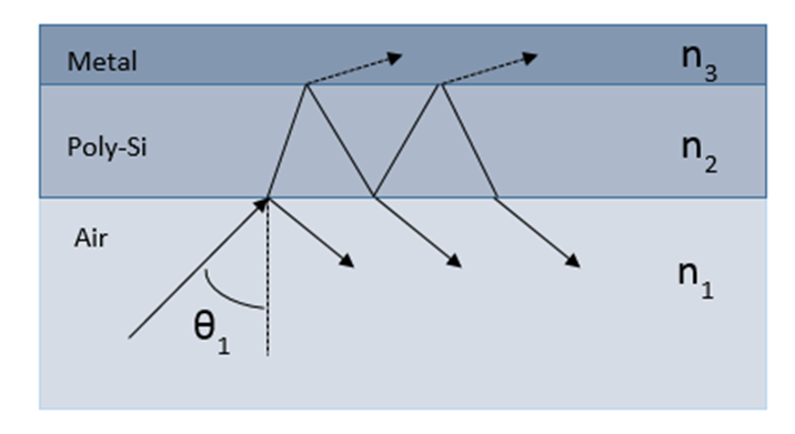 | Figure 2. Three-layer structure used in calculation of transmission and reflection Medium 1 is air, medium 2 is poly-Si, and medium 3 is a thin metal layer |
 | (1) |
3. Results
- The results presented in this section are twofold: An absorption factor of 96% was reached. A generalization of these results and properties over a wide frequency spectrum was also achieved. Based on the results of previous work in the terahertz spectrum (0.1-10 THz) [8], through a post-optimization process, we extended the high absorption properties both in the mid and the long wavelength infrared spectrum (3 to 14 μm). As a result, the developed double-layered absorber with enhanced TCR retains the ability to absorb 96% and reflects less than 1% of the incident power over a wide frequency spectrum and can be considered as a good candidate to operate as the active pixel element of a microbolometer.
3.1. The High Absorption Capability and the Fine-tuning Process
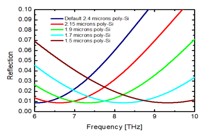
- Based on previous experimental results, presented in [8], the absorber was initially adjusted at the frequency of 6 THz, consisting of a glass layer (BK 7) with 4.9 μm thickness and refractive index of 2.52, on top of any thin metal film of sheet resistance of 55 [Ω/square]. The absorption achieved was up to 86% [8]. Taking advantage of the fact that increasing the refractive index of the dielectric medium, a respective increase in the absorption occurred, we substituted the glass layer with a material of high refractive index (diluted poly-Si with n=5.2) and we reiterated the fine-tuning process as described in [8]. The result of that process is illustrated in Fig. 3, showing that for a poly-Si layer with 2.4 μm thickness at the frequency of 6 THz and under normal incidence, near 100% of absorption has been achieved.
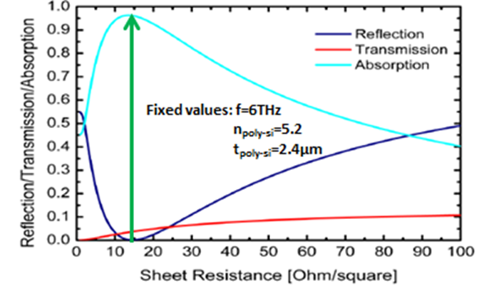 | Figure 3. Reflection / Transmission / Absorption of the double-layered absorber at 6 THz as a function of metal’s sheet resistance |
 | Figure 4. Reflection of the double-layered absorber as a function of frequency |
3.2. Frequency Dependence and a Wide-spectrum Linear Equation
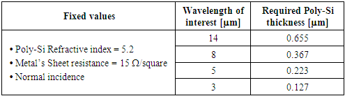
- Due to our interest in examining the frequency dependence of absorptance characteristics of the double-layered absorber, we observed the uniqueness of the high absorption behavior by an individual absorption peak (at 6 THz) through all the THz spectrum, as illustrated in Fig. 5. In addition, when we had calculated the frequency shifts with variation of glass thickness, we observed a linear relation [8].
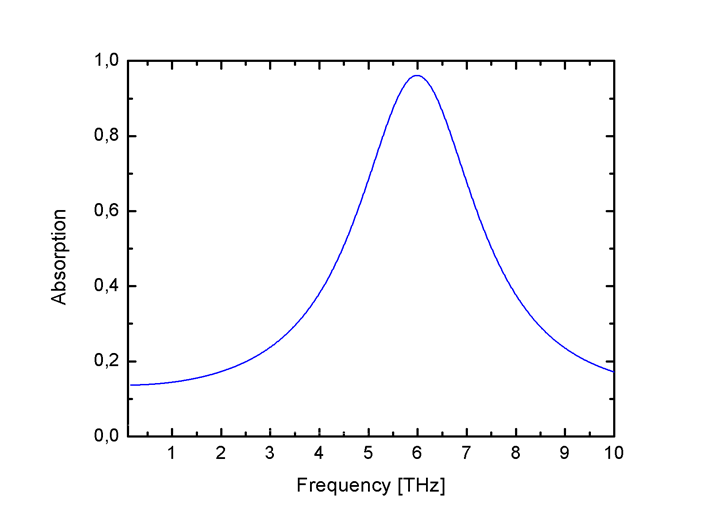 | Figure 5. Absorption of the double-layered absorber as a function of frequency |
|
 | (2) |
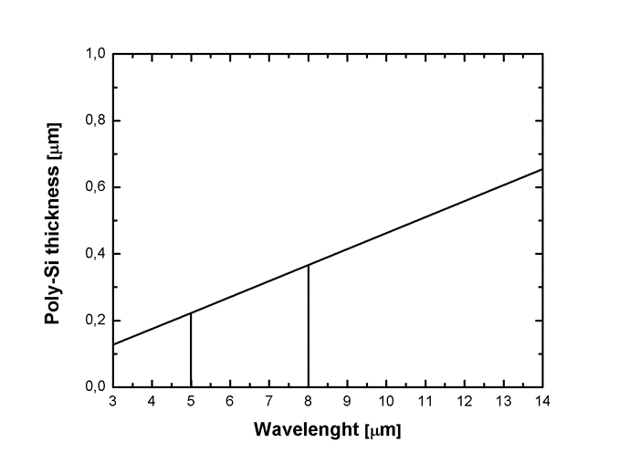 | Figure 6. The linear connection between silicon thickness and wavelength of interest |
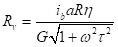
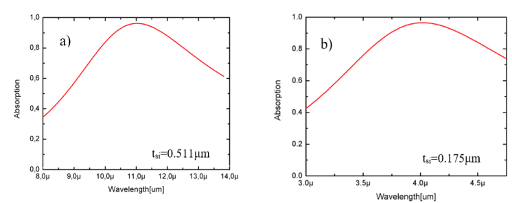 | Figure 7. Absorption of the double-layered absorber as a function of MWIR (a) and LWIR (b) spectral regions |
4. Microbolometer Integration
- To date, a variety of materials have been used as detection elements in microbolometers. The sensitive region of a pixel is a thin membrane jointly composed of an absorbing layer and a high temperature coefficient of resistance (TCR) layer [14]. For every material in use, it is desirable to conform to specific standards. Those standards are related to both the performance, microfabrication constraints and the integration capabilities of the microbolometric pixel to a wider detection scheme.
4.1. Microbolometric Standards
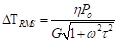
- Two of the most critical metrics for any thermal detection system are the voltage responsivity and the root mean square of sensitivity. Assuming that the pixel temperature increases and decreases are modulated at frequency ω, the above quantities will be given, respectively, by the following equations [15]:
 | (3) |
 | (4) |
 is the temperature coefficient of resistance, R is the initial microbolometer resistance, η is the fraction of incident radiation that is absorbed by the pixel’s sensitive layer, P0 is the incident power, G is the thermal conductance of the pixel and τ is the time constant of the detector.The materials used, should have both the ability for integration with CMOS at relatively low temperatures and low 1∕f noise [17]. The noise equivalent temperature difference of state-of-the-art uncooled bolometers is typically limited by the 1∕f noise from the bolometer’s temperature-sensing material [17, 18].
4.2. The ‘’Hybrid’’ Nature of the Absorber
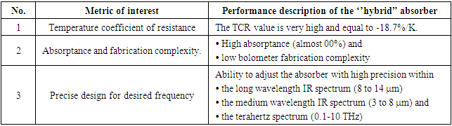
- Both the diversity of the microbolometer designs and the material choice (e.g. vanadium oxide (VOx), amorphous silicon (α-Si) and metals), are basic parameters for achieving the desired microbolometer functionality. Through post optimization process, carried out in the present research, one can highlight the ‘’hybrid’’ nature of the absorber comprised of a thin metal layer and a high-TCR layer with an index of refraction of 5.2, which can reach an absorption up to 96%. The ‘’hybrid’’ nature of the absorber, allows for a choice of the layer functioning as the active pixel element of the microbolometer configuration. The choice may be between a thin metal layer or a poly-Si layer. The advantages afforded by this choice are described in the following paragraphs.To date, much work has been done on the performance optimization of each type of microbolometer. The first state-of-the-art type consists of a microbolometric pixel element with thin metal layers [19-23], while the second (and widely used) state-of-the-art type consists of a microbolometric pixel element with high TCR (VOx or amorphous silicon, involving metamaterials too) [24-34].Considering the presented ‘’hybrid’’ absorber (with the active sensing element selected to be the metal), as the case of a state-of-the-art microbolometric pixel element with thin metallic layers, the hybrid absorber allows freedom of choice of metal, provided that it possesses Rs = 15 Ω / square. With that in mind, it is possible to choose the metal element to be Ti, which has significantly lower thermal conductivity and relatively high temperature coefficient of resistance (0.35% / K). Through the use of the ‘’hybrid’’ absorber, the absorption level is almost 100% of incident radiation, without the need of a resonant optical cavity sub-assembly. In addition, the use of optical cavity sub-assembly increases both the complexity and the total cost of the bolometric configuration in general. At the end, by using the element proposed, this optimal resonant absorptance can be adjusted with high precision within the medium wavelength IR spectrum (3 to 8 μm), the long wavelength IR spectrum (8 to 14 μm) and the terahertz spectrum (0.1-10 THz). An overview of the benefits that emerge from the use of the ‘’hybrid’’ absorber when the thin metal layer is used as the sensing pixel element, is shown in the following table:
|
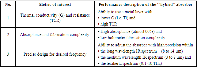
|
5. Discussion and Conclusions
- In this paper, recent THz and IR detection results for a double-layered absorber consisting of a thin metal layer located on a poly-Si medium were presented. The absorption characteristics were calculated and post-optimized through the appropriate parameterization, with designed resonant peaks covering the whole THz spectrum (0.1 - 10 THz) and both the mid and the long wavelength IR region (3 - 14μm). If the proposed ‘hybrid’ absorber implemented as an active pixel element of a microbolometer, it could be accurately adjusted to the desired wavelength of incident radiation with high accuracy. When integrated with the existing microbolometer technology, numerous advantages emerge. Overall, a new approach for efficient microbolometers is proposed. The advantages of the presented configuration are summarized in: low cost, efficiency, precision and broad adjustability. The use of the wide-spectrum linear equation, as illustrated in paragraph 3.2, shows that the developed sensing element can be used at any resonant frequency of interest. For these reasons, this configuration can be considered a promising candidate for integration into currently used microbolometer configurations.