Charles U. Ndujiuba1, Samuel N. John1, Taofeek O. Bello2
1Electrical & Information Engineering, Covenant University, Nigeria
2Electrical & Electronics Engineering, University of Lagos, Nigeria
Correspondence to: Charles U. Ndujiuba, Electrical & Information Engineering, Covenant University, Nigeria.
| Email: |  |
Copyright © 2016 Scientific & Academic Publishing. All Rights Reserved.
This work is licensed under the Creative Commons Attribution International License (CC BY).
http://creativecommons.org/licenses/by/4.0/

Abstract
This paper proposes a duplexer design with two microstrip bandpass filters which are designed using Open Loop Square Resonator method and matching between these two bandpass filters using T-junction matching devices. Both seven-pole band-pass filters for the receiver at 1710-1785 MHz and transmitter at 1805-1880 MHz, with fractional bandwidth of 4.29% and 4.07% respectively, of the center frequencies were implemented by resonators and admittance inverters with a 0.1dB ripple in the pass band. Agilent Advance Design Simulation (ADS) EM simulator was used in obtaining the dimensions of the resonators, extraction of coupling coefficients and external quality factors associated with the microstrip design. Results obtained showed a return loss of about 8dB, insertion loss less than 1dB and isolation between transmit and receive filters of about 32dB. The choice of the square open-loop resonators against parallel coupled lines is to avoid the inherent shift in the center frequency of the parallel coupled technique. The designed microstrip duplexer filter showed good agreement with theoretical results.
Keywords:
Duplexer, Microstrip filter, Fractional bandwidth, Resonators
Cite this paper: Charles U. Ndujiuba, Samuel N. John, Taofeek O. Bello, Design of Duplexers for Microwave Communication Systems Using Open-loop Square Microstrip Resonators, International Journal of Electromagnetics and Applications, Vol. 6 No. 1, 2016, pp. 7-12. doi: 10.5923/j.ijea.20160601.02.
1. Introduction
Microwave communication systems require, especially in satellite and mobile communications, high-performance narrow-band bandpass filters having low insertion loss and high selectivity together with linear phase or flat group delay in the pass-band. These filters form an integral part of power amplifiers at the transmitter and receiver in radio systems.The miniaturization of electronic components has received a lot of attention in the last decades due to the rapid development of the telecommunication industry. Traditional high performance waveguide and dielectric resonator filters are usually too heavy and bulky for most applications like tower-top mounting in base stations [1]. In radar and radio communications systems, a duplexer allows for a bi-directional (duplex) communication over a single path. This device isolates the receiver from the transmitter while permitting them to share a common antenna. One major problem associated with this design is the degradation in filter selectivity. Practical RF and Microwave filters realized with low-Q reactive elements not only have high insertion loss, but also have rounded passband corners, the positions of the poles and zeros displaced, and the desired centre frequency shifted. These defects are particularly serious in duplexers where isolation between the transmit and receive paths are required to be high, and multiplexers where adjacent channels must be sharply and accurately defined.Duplexer designed for the base station antenna allows the combination and separation of the signals in band1 and band2 wireless bands. To minimize band inter-reaction, the inputs are all isolated and have minimal insertion loss over their respective frequency bands. The design ensures low-passive intermodulation. An efficient duplexer needs high isolation between two passband frequencies to avoid interference of signal from one port to another. The implementation of the duplexer filter on a microstrip structure will help to achieve a filter with a compact size and high performance. The duplexer consists of two bandpass filters which could either be realized using lumped components or distributed components. Lumped components consists of discrete elements like inductors, capacitors etc. Distributed elements consist of transmission line sections which simulate various inductance and capacitance values. It is hard to realize filters with lumped elements at high frequencies in the GHz range, the dimensions of the electronic components are comparable with the wavelength of the signal as a result of which there could be distributed effects. However transmission line filters are easy to implement and are compact at these frequencies [2]. A bandpass filter allows transmission of frequencies in the passband and attenuates frequencies in the stopband. The circuit synthesis and microstrip realization of the duplexer filter is presented in this paper.
2. Filter Design Using Lumped Components
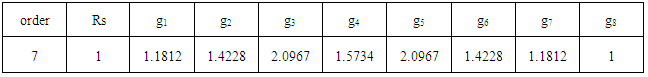
The synthesis of bandpass filter often starts with a lowpass filter which is achieved by frequency transformation. The design in this paper is two band pass filters with the same characteristics but different band responses of 1710-1785MHz and 1805-1880MHz, for the receive and transmit path, respectively. Chebyshev lowpass filter prototype is adopted in this paper because the attenuation of the Chebyshev filter is steeper in amplitude versus frequency curve [3] and hence requires only fewer stages for the same attenuation demanded. A. Design of Prototype Low Pass Filter Prototype filter acts as template to provide a modified filter design for particular application. A normalized lowpass filter prototype in which the elements involved are normalized so as to make the source resistance to be equal to 1Ω and a cut-off frequency of 1rad/s. For a 7th order (n = 7) Chebyshev filter where the first element is an inductor. The element values for the low-pass circuit are given in table 1 and represented in figure 1.Table 1. g values of a 7th order chebyshev normalised lowpass filter
 |
| |
|
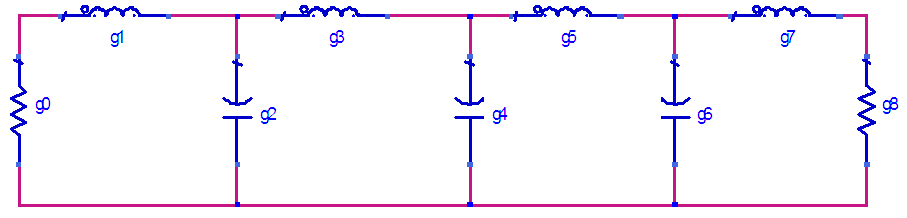 | Figure 1. Prototype Lumped Element Low pass Filter |
B. Conversion to shunt only using J invertersImmittance inverters play a very important role in filter design. They are used to transform a filter circuit into an equivalent form that can be easily implemented using various microwave structures [4]. Immittance inverters are either impedance or admittance inverters. In this design the J-inverters (an admittance inverter) is used to convert the lumped element low-pass filter to a design that eliminates the inductors and contains shunt only capacitors as shown in figure 2.A further transformation to make all the values of the shunt capacitor to be equal in figure 3 was carried out using the equation 1.0 to obtain values of J as shown in the table 2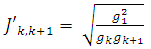 | (1) |
where k = 1, 2 , 3, ...6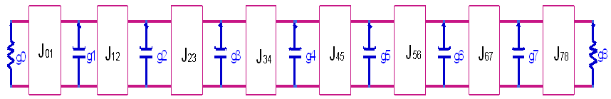 | Figure 2. Shunt only normalised lowpass filter |
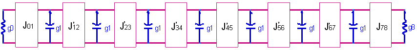 | Figure 3. Lowpass filter with equal shunt value of |
Table 2. J inverter values with equal g
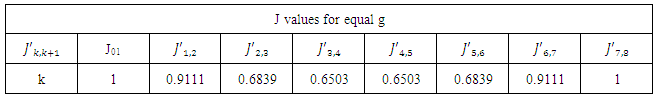 |
| |
|
C. Impedance and Frequency scalingThe low-pass filter prototypes are circuit designed for unity cutoff frequency and unity source and load impedance. The circuit is desired to resonate at the bandpass cutoff frequency and have a source and load resistance of 50Ω, an impedance and frequency scaling is carried out using equation 2.0, new values of g1 and J are obtained. It can be seen from the transformation that the J inverters are only affected by impedance scaling and not affected at all by the frequency scaling.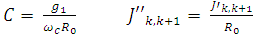 | (2) |
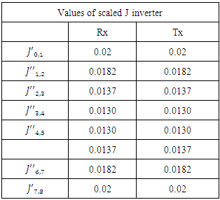
where R0 is 50Ω and 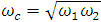 .Table 3 presents the scaled value of the J inverter
Table 3. Values of scaled J inverter
 |
| |
|
D. Band pass transformationLow-pass prototype filter designs can also be transformed to an equivalent bandpass filter. During the transformation process, the shunt capacitor of the low-pass prototype is converted to series LC circuits having element value given by equation 3.0. The values of L and C is given in table 4 and represented in figure 4.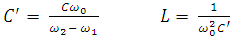 | (3) |
Table 4. Values of bandpass capacitor and inductor
 |
| |
|
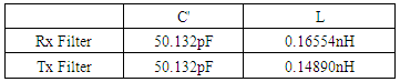
The J inverters are converted to  capacitors in circuit design. The use of capacitor elements to represent admittance is seen as analogous to modeling an electric coupling occurring between resonators [5]. The capacitances representing the J inverter were calculated using the equation 4.0 and presented in table 5.
 | (4) |
Table 5. Values of the -capacitor
 |
| |
|
Each filter was simulated to give a response shown in Figures 9 and 10.The duplexer formed from these two bandpass filter was obtained by using a T-junction between the filters. A combination of the Rx and Tx filter was carried out using an input ideal transmission line of 50Ω connected to the J inverter (pi capacitors) for the Rx and for the Tx filter. The two 50Ω transmission lines from the Rx and Tx filter were both connected together to another 50 Ω transmission line forming a T junction network which forms the duplexer circuit shown in the figure 5.The response obtained after tuning in ADS is given below in figure 11.E. Design of Matching CircuitThe Matching network and combining circuit ensure that both filters match the antenna and have good isolation between them. The T-junction may be the most popularly used combining circuit. The length and width of its two branches must be chosen carefully. The T-shaped resonator is composed of a three-section transmission line. Each section has an adjustable characteristic impedance and length. The most intuitive approach is to combine two BPFs with a T-junction /Y-junction. The method, which features the Filter A (Filter B) an open-circuit-load shunted to the Filter B (Filter A) at the frequency of the latter, is adopted to Figure the dimensions of the connecting line for reducing the mutual loading effect between the Filters. We calculate these three impedances by using T-Matching networks impedance formulas. 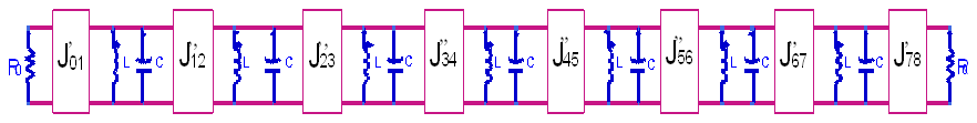 | Figure 4. Equivalent circuit of bandpass filter |
 | Figure 5. Circuit synthesis of duplexer filter |
3. Filter Design Using Microstrip Lines
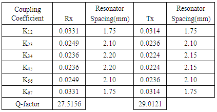
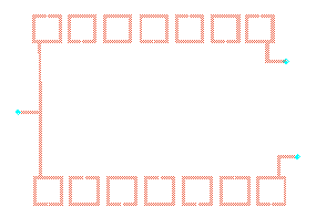
Various topologies are available in the implementation of microstrip bandpass filters [5-7]. In this paper the focus is on square open loop resonators using mixed coupling with the following substrate specification:Substrate Material = RT/DurioidDielectric constant (ɛr) = 10.8Substrate thickness = 1.27mmCharacteristics impedance = 50ΩLoss Tangent = 0.004In this section a square open loop geometry shown in figure 8 of length 33.5mm and 31.7mm both with width 1mm was used to design a 7th order filter of the receive and transmit arm respectively, which resonated at the center frequency of the individual bandpass filters.Mixed coupling between the resonators and external coupling was extracted using the ADS EM simulator, using the procedure described in [5]. The inter resonator spacing shown in the figure 6 is given in the table 6.The length of the transmission line connecting each filter to the T-junction of the duplexer was calculated, simulated and tuned to obtain the desired response. The obtained length for each filter was 63.7mm for the receive band, and 87.0mm for the transmit band. | Figure 6. Square open loop geometry |
 | Figure 7. Mixed coupling between resonator |
Table 6. Coupling coefficients between the frequency bands
 |
| |
|
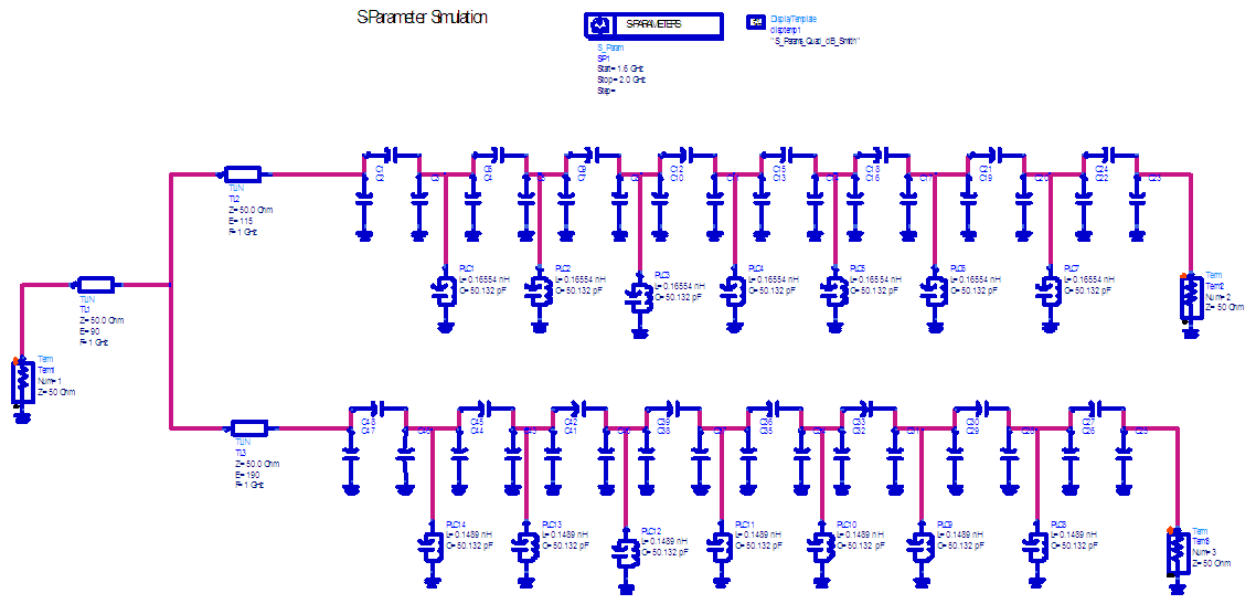
 | Figure 8(a). Schematic of the microstrip duplexer filter |
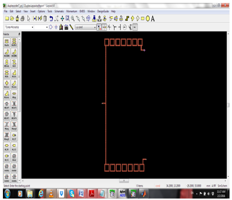 | Figure 8(b). Layout of the Microstrip duplexer filter |
4. Simulation and Results
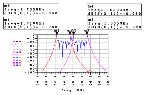
The simulated result of the duplexer filter designed with two bandpass filters gave a return loss of about 8dB and an insertion loss less than 1dB. The isolation between the filters was about 32dB. The result was obtained after a minor optimization of the microstrip length that formed the T-junction. A comparison between the simulation of the circuit synthesis and microstrip duplexer showed similarities between the two duplexers. The return loss of the circuit was about 15dB while that of the microstrip realization was 8dB. The insertion loss for both cases was less than 1dB.(a) Simulation Results of Lumped Element Realization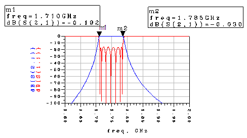 | Figure 9. Response of the Receive Filter using lumped elements |
 | Figure 10. Response of the Transmit Filter using lumped elements |
 | Figure 11. Response of the Duplexer using lumped elements |
(b) Simulation Results using Microstrip Realization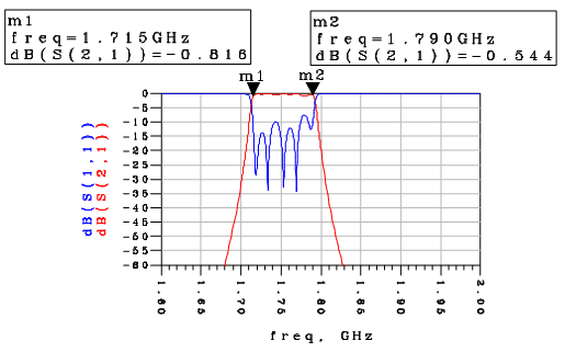 | Figure 12. Response of the Receive Filter using microstrip resonator |
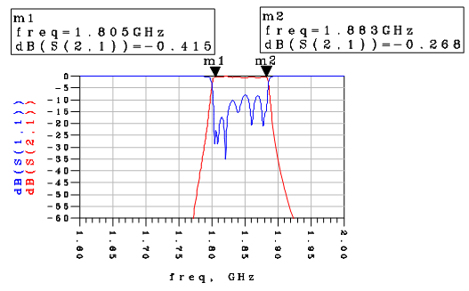 | Figure 13. Response of the Transmit Filter using microstrip resonator |
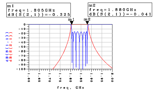
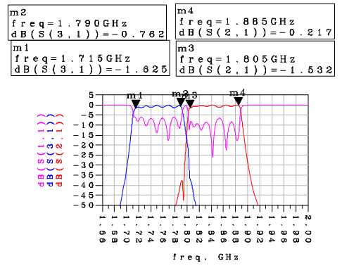 | Figure 14. Response of the Duplexer using microstrip resonator |
(c) Isolation between Rx and Tx Filter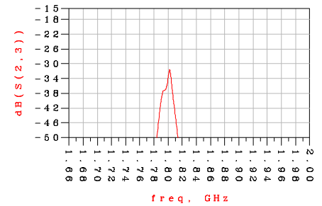 | Figure 15 |
5. Conclusions
A simple procedure, for designing a microstrip duplexer, and ensuring the selectivity of the individual filters, has been shown. The inband response of the filters was not compromised and the results of theoretical calculations are in close agreement with the simulation results. It is noticed that the microstrip duplexer can further be optimized to achieve as close as possible to the circuit synthesis of the lumped components. The technique enabled us to obtain the prescribed filter specifications, while the passband loss can be compensated by an active device, such as negative resistance. Simulation results were obtained using ADS tool.Microstrip technology is proposed because it provides a better insertion loss, better return loss and good isolation between the passbands. The isolation obtained between the two operating bands is better than -32dB and the overall insertion loss obtained is -0.4 dB. The overall return loss is less than -20 dB.The open-loop square resonator was chosen over the popular parallel-coupled technique to minimize the shift in the center frequency that characterizes the parallel-couples method. However, this limitation can be overcome by the use of predistortion technique [11].
References
| [1] | R. R. Mansour, “Filter technologies for wireless base stations,” IEEE Microwave Magazine, vol. 5, no. 1, pp. 68–74, Mar. 2004. |
| [2] | Jolly Rajendran, Rakesh Peter, and K. P. Soman, Design and Optimization of Band Pass Filter for Software Defined Radio Telescope, International Journal of Information and Electronics Engineering, Vol. 2, No. 4, July 2012. |
| [3] | D. M. Pozar, “Microwave Engineering,” 2nd ed New york, Wiley, 1998, pp. 367-368. |
| [4] | S. Srinath, Design of 4th Order Parallel Coupled Microstrip Bandpass Filter at Dual Frequencies of 1.8 GHz and 2.4 GHz for Wireless Application, International Journal of Innovative Research in Computerand Communication Engineering, Vol. 2, Issue 6, June 2014. |
| [5] | J.S. Hong and M. J. Lancaster, “Couplings of microstrip square open-loop resonators for cross-coupled planar microwave filters,” IEEE Trans. Microwave Theory Tech., vol. 44, pp. 2099–2109, Nov. 1996. |
| [6] | Ralph Levy and Seymour B Cohn, “A History of Microwave Filter Research, Design, and Development”, IEEE Transactions on Microwave Theory and Techniques, Vol. Mtt-32, No. 9, Septemrer1984. |
| [7] | Shakeri, M; Bavafa, M., “Design of 2.4 GHz bandpass filter using the closed loop resonator with the compound stub”, International Conference on Microwave and Millimeter Wave Technology, pp. 2048–2050, May 2010. |
| [8] | Gupta, K. et al (1996) Microstrip Lines and Slotlines, 2nd Edition, Norwood: Artech House Inc. |
| [9] | Hong, J. & Lancaster, M. (2001) Microstrip filters for RF/Microwave application, New York: John Wiley & Sons. |
| [10] | Chen, C. et al (2006) ‘Microstrip Diplexers Design with Common resonator sections for compact size but high isolation’, IEEE Transactions on Microwave theory and Techniques, Vol.54, No.5, Pages 1945-1952. |
| [11] | Ndujiuba C.U. and Khanifar A ‘The Design of MMJC Filters Using Predistortion Technique’, 28th European Microwave Conference Amsterdam 1998, pages 379-384. |

 Abstract
 Reference
 Full-Text PDF
 Full-text HTML